Lead fluoride Cherenkov detector read out by avalanche photodiodes for measuring the intensities of pulsed antiproton beams
Abstract
A Cherenkov detector based on an array of five lead fluoride (-PbF2) crystals of size 30 mm30 mm160 mm read out by reverse-type avalanche photodiodes (APD’s) of active area 10 mm10 mm was used to measure the flux of secondary particles emerging from the annihilation of pulsed beams of antiprotons at the Antiproton Decelerator of CERN. We compared the relative photon yields of radiators made of -PbF2, fused silica, UV-transparent acrylic, lead glass, and a lead-free, high-refractive-index glass. Some p-i-n photodiodes were also used for the readout, but the output signals were dominated by the nuclear counter effect (NCE) of secondary particles traversing the 300 thick depletion regions of the photodiodes. Smaller NCE were observed with the APD’s, as the maximum electronic gain in them occurred predominately for electron-ion pairs that were generated in the thin -type semiconductor layer that proceeded the p-n junction of high electric field where amplification took place.
keywords:
Lead fluoride , Cherenkov detector , antiproton , avalanche photodiode1 Introduction
The Atomic Spectroscopy and Collisions Using Slow Antiprotons (ASACUSA) collaboration has recently measured the cross sections of antiprotons with an incident kinetic energy MeV annihilating via in-flight nuclear reactions in carbon, Mylar, nickel, tin, and platinum targets [1, 2, 3]. Measurements of were also attempted on keV antiprotons annihilating in carbon, palladium, and platinum target foils of sub-100 nm thicknesses [4, 5, 6]. These experiments were carried out at the Antiproton Decelerator (AD) of CERN using –120 ns long pulsed beams that contained between and antiprotons. The arrival of individual antiprotons at the target could not be resolved. We instead determined the relative intensity and temporal structure of the beam by using acrylic Cherenkov detectors to measure the flux of secondary charged particles (mostly charged pions, muons, and electrons) that emerged from the simultaneous annihilations in the apparatus. These past experiments utilized fine-mesh photomultiplier tubes [7] which had signal responses that were highly linear to read out the Cherenkov radiators.
| Photodiode | Area | Eff. thickness | Capacitance | Cutoff freq. | Spect. response |
|---|---|---|---|---|---|
| (mmmm) | (m) | (pF) | (MHz) | (nm) | |
| S8664-1010 (APD) | 1010 | 270 | 11 | 320–1000 | |
| S3204-08 (p-i-n) | 1818 | 300 | 130 | 20 | 340–1100 |
| S3590-08 (p-i-n) | 1010 | 300 | 40 | 40 | 340–1100 |
In this paper, we describe a different Cherenkov detector that consisted of an array of five lead fluoride crystals in the cubic phase (-PbF2) [8, 9, 10, 11] of size 30 mm30 mm160 mm. The arrival of antiproton pulses at the experimental target produced an intense flash of Cherenkov light in each crystal; this was measured by a reverse-type [12, 13, 14, 15, 16] avalanche photodiode (APD) of active area 10 mm 10 mm. These crystals are sensitive to both the charged secondary particles and -rays [7] that emerge from antiproton annihilations, and are expected to have a higher light yield compared to Cherenkov detectors based on acrylic radiators of the same size. Other advantages of the detector include its compact size and insensitivity to magnetic fields, which may allow its use in experiments involving magnetic Penning traps within the physics program of the AD [17]. The radiation-hard nature of the -PbF2 crystals may allow their use in measuring high-intensity beams of electrons in laser spectroscopy experiments of metastable pionic helium atoms [18]. We compared the light yields of Cherenkov radiators made of -PbF2, fused silica, acrylic, lead glass, and a lead-free, high-refractive index glass against antiproton annihilations. We also attempted to use p-i-n photodiodes [19] for the readout, but the waveform of the output signals contained a dominant background that arose from the nuclear counter effect (NCE) of secondary particles traversing the thick depletion regions of these detectors [20, 21]. The relative size of the NCE was much smaller in reverse-type APD’s, because the maximum electronic gain occurred predominantly for those electron-ion pairs that were generated in the thin -type semiconductor layer that proceeded the p-n junction of high electric field where amplification took place [12, 13, 14, 15, 16, 21]. The detector was recently used in an experiment to determine the cross section of 5.3 MeV antiprotons annihilating in a carbon target [3].
Since the 2000’s, -PbF2 crystals have been used in electromagnetic calorimeters with high timing resolutions. The A4 collaboration used 1022 crystals of lengths between and 180 mm, in a parity-violating, electron-scattering experiment that was carried out at the Mainz Microtron (MAMI) facility [11, 22]. Each crystal was read out by a photomultiplier tube with 10-stage, line focusing dynodes. The muon g-2 experiment at Fermilab utilized crystals of size 25 mm25 mm140 mm, which were read out by arrays of 16 silicon photomultipliers (SiPM’s) of active area 12 mm12 mm [23, 24]. Positrons of energy GeV that emerge from decays in a storage ring were reconstructed with an energy resolution of and a timing resolution ps. A positron annihilation lifetime spectroscopy (PALS) experiment used the -PbF2 crystals to detect 511 keV gamma rays with a timing resolution ns [25].
The advantages of -PbF2 crystals include a high refractive index () and density ( g/cm3), significant transmission at ultraviolet wavelengths nm, radiation hardness (– rad) [8, 26], and a small radiation length ( mm) and Moliere radius ( mm). On the other hand, the light yield of -PbF2 is much smaller than those of scintillators such as lead tungstate (PbWO4) and thallium activated cesium iodide [CsI(Tl)]. For each MeV of energy deposited in a -PbF2 crystal, a photomultiplier coupled to it typically detects –1.9 photoelectrons [11]. It is difficult to grow large ( mm) crystals of high transparency and optical uniformity [27, 28, 29]. It was noted that when oxygen impurities were allowed to diffused into the crystals during their growth, regions that consist of lead oxide, lead fluoro-oxide, or the opaque, orthorhombic phase of lead fluoride (-PbF2) were formed. These appeared as scattering centers and inclusions that could reduce the collection efficiency of the Cherenkov light. It has also been reported that when exposed to a high-humidity environment, the surfaces of the crystals changed into a frosty-whitish appearance [28, 29].
2 Detector
2.1 Construction
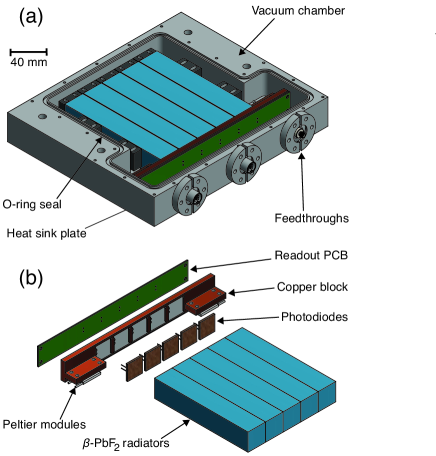
The five -PbF2 crystals of size 30 mm30 mm160 mm (see Fig. 1) were wrapped in two layers of a polyvinylidene fluoride membrane with 0.45 pores (Millipore Immobilone-P), which constituted a diffusive reflector. A silicon APD of active area 10 mm10 mm (Hamamatsu Photonics S8664-1010, see Table 1) was attached to one end of each crystal. The five APD’s in the array were thermally anchored on a 200 mm long copper block using thermal paste (Electrolube HTCP). A two-terminal, temperature-to-voltage transducer (Analog Devices AD590MH) was also glued to the block using an epoxy adhesive that had a high thermal conductivity (Henkel Loctite Stycast 1266). This assembly was cooled to a temperature ∘C with a stability of ∘C, using two Peltier thermoelectric modules (Adaptive ET-03-10-13-RS) of size 30 mm15 mm and cooling power W that were regulated by a proportional–integral–differential controller (Thorlabs TED200C) and a separate 5 W direct current (DC) power supply. The electronics for biasing the photodiodes, amplifying the output signals, and providing the low-noise, regulated DC power sources of V and V were integrated on a four-layered printed circuit board (PCB) of size 30 mm200 mm. This PCB made of 1.6 mm thick glass epoxy (Panasonic Electronic Works R1705) was also mounted to the copper block using four Teflon standoffs that helped to thermally isolate it from the block.
The detector was housed in a 290 mm245 mm50 mm aluminum chamber of wall thickness mm. The chamber was hermetically sealed and purged with nitrogen to prevent condensation on the cooled photodiodes and -PbF2 crystals that may arise from the high humidity in the vicinity of the cryogenic target. The chamber also shielded the photodiodes against the electromagnetic interference of frequency range –200 MHz that was emitted from the AD and radiofrequency quadrupole decelerator (RFQD) [17]. Detector modules which employed silicon p-i-n photodiodes of active area 18 mm18 mm (S3204-08) or 10 mm10 mm (S3590-08) instead of the APD were also constructed (Table 1). The photodiodes were protected by thin windows of epoxy resin.
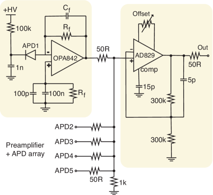
A bias voltage V was applied to the cathode terminal of each APD through a low-pass filter that consisted of a k thin metal film resistor and a nF radiofrequency mica capacitor (see Fig. 2). The anode terminals were connected to transimpedance preamplifiers that contained an operational amplifier (Texas Instruments OPA842IDB) with a gain bandwidth product of MHz, input voltage noise 2.6 nV/, low distortion, and a DC voltage offset mV. A feedback resistor 1 k which corresponded to a photocurrent-to-voltage conversion ratio V/A was chosen to provide the best dynamic range for measuring the Cherenkov signals with typical amplitudes of 20–40 mV. As the APD’s had a large terminal capacitance pF, a compensating feedback capacitor pF was added to avoid excessive ringing and oscillation of the output signal, and obtain a flat frequency response with a -3dB corner frequency MHz. For reading out the S3204-08 p-i-n photodiodes of pF, the feedback elements were changed to values k and pF which provided the best compromise between a higher gain V/A, corner frequency MHz, and the stability of the transimpedance preamplifier. For the smaller p-i-n photodiodes (S3590-08) of pF, an operational amplifier (OPA843IDB) of larger gain bandwidth product MHz in conjunction with feedback values k and 2 pF were used to obtain a -3dB corner frequency MHz.
The output signals of the five transimpedance preamplifiers were summed using a resistor network, and amplified by a non-inverting follower of gain 2 which was based on a bipolar operational amplifier (Analog Devices AD829AR) with an input voltage noise nV/. This resulted in an output signal of typical amplitude –400 mV into a 50 impedance, which was superimposed on a DC offset. The signal was transmitted out of the chamber using a SMA-type coaxial vacuum feedthrough, and its analog waveform recorded by a digital oscilloscope of analog bandwidth GHz, digital sampling rate Gs/s, and a vertical resolution of 8 bits (Lecroy Waverunner 640Zi). The V and V DC power needed for the amplifiers were generated by four linear regulators (Linear Technology LT1965IDD and LT3015IDD) and passed through some electromagnetic interference filters (Murata BNX002). The linear regulators were supplied with source voltages that were adjusted slightly ( V) above their regulated output voltages. This helped to minimize the heat dissipation in the chamber.
2.2 Cherenkov radiators
| Radiator | Refractive index | Density | Radiation length | UV cutoff |
|---|---|---|---|---|
| (g/cm3) | (mm) | (nm) | ||
| -PbF2 (lead fluoride) | 1.82 | 7.77 | 9.3 | |
| T-4040 (fused silica) | 1.49 | 2.2 | ||
| Clarex S-0 (acrylic) | 1.46 | 1.18 | ||
| SF57HTultra (lead glass) | 1.85 | 5.51 | 15 | |
| S-TIH53W | 1.84 | 3.54 |
The -PbF2 crystals were grown using the Bridgman method and all surfaces polished by the Shanghai Institute of Ceramics, Chinese Academy of Sciences (SICCAS). The crystals were specified by the manufacturer to be without cracks or scratches longer than 10 mm and deeper than 2 mm, and no inclusions, scattering centers, or microcracks observable with the naked eye. Cherenkov radiators of the same size made of fused silica (CoorsTek T-4040), UV transparent grade acrylic plastic (Nitto Jushi Kogyo Co. Clarex S-0), high transmission grade lead glass (Schott AG SF57HTultra), and Ohara S-TIH53W glass were also manufactured (see Table. 2). The last of these was a lead-free glass with a high refractive index , density g/cm3, and partial dispersion of Abbe number . X-ray photoelectron spectroscopy measurements on ground samples of the glass showed that it contained barium, titanium, and niobium oxides. These “eco-friendly” alternatives to conventional flint glass generally have reduced transmission at blue and UV wavelengths. The surfaces of the fused silica, lead glass, and S-TIH53W glass radiators were optically polished to a quality that was specified to be scratch-dig 60-40 and flatness of peak-to-valley wave.
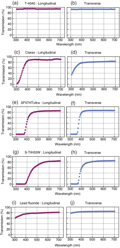
The optical transmissions (Fig. 3) of each radiator along its longitudinal (i.e., long) axis, and at four positions [indicated by arrows labeled T1, T2, T3, and T4 in Fig. 4(a)] parallel to its transverse (short) axis at wavelengths between and 700 nm were measured using a photospectrometer. The device was of single beam type and included a xenon halide lamp as the light source. No position-dependent variations over T1–T4 were seen in the transverse transmissions of the fused silica, acrylic, lead glass, and S-TIH53W radiators, and so we plotted the typical values for each material in Figs. 3(b), 3(d), 3(f), and 3(h), respectively.
The fused silica radiators [Figs. 3(a)–(b)] showed high transverse and longitudinal transmissions of over the entire range of measured wavelengths. The majority of the losses were caused by the reflections at each glass-to-air interface, whereas the attenuation in the glass was negligible. The transverse and longitudinal transmissions of the acrylic radiator at visible wavelengths –700 nm were slightly lower at and , respectively [Figs. 3(c)–(d)]. Significant reductions of the transmissions to and were seen at a UV wavelength nm.
The lead glass radiators [Fig. 3(e)] retained transmissions of over the visible wavelengths nm, which rapidly decreased to and at the UV wavelengths nm and nm, respectively. The transverse transmission [Fig. 3(f)] was somewhat higher: , , and at the respective wavelengths nm, nm, and nm. The S-TIH53W radiator had a slightly yellowish color [Figs. 3 (g)–(h)], and the highest absorption among the materials studied here. The longitudinal transmissions at wavelengths nm and 405 nm were and , respectively. The transverse values at nm and 380 nm were and , respectively.
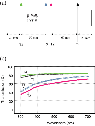
The UV transmission of the -PbF2 crystals were lower compared to fused silica, but higher than the other three materials studied here [Figs. 3(i)–(j)]. Small, white scattering centres along the surfaces of the -PbF2 crystals caused significant variations in the optical transmission: in one sample, transmissions of 74%, 35%, 32%, and 78% were measured at the respective positions T1, T2, T3, and T4 [Fig. 4(b)]. The longitudinal transmission was typically 80% at visible wavelengths –700 nm, and at nm.
2.3 APD’s and p-i-n photodiodes
The S8664-1010 silicon APD’s [15, 16] (Table 1) of active area 10 mm 10 mm were previously used to read out CsI(Tl), BGO, and GSO(Ce) scintillators that emit at blue and green wavelengths [14, 30, 31]. The quantum efficiencies specified at wavelengths nm, 420 nm, and 600 nm were , , and , respectively. The APD’s were of the so-called reverse type, where the p-n junction of high field in which multiplication takes place was typically located about from the illuminated surface of the sensor [12, 13, 14, 15, 16]. Visible photons were absorbed and generated electron-hole pairs within the first few microns of the depletion region. These electrons were collected and underwent multiplication with the highest gain. Although charged particles, X-rays, and neutrons traversing the APD generated primary ion pairs over the entire width of the photodiode, only those pairs that originated in the thin p-type layer preceding the high-field p-n junction underwent high-gain multiplication. This lead to a small ( m) effective thickness of the device with regards to the nuclear counting effect (NCE) against ionizing radiation, which was measured using a 90Sr source [14].
The S3204-08 silicon p-i-n photodiode, on the other hand, had an active area of 18 mm 18 mm, depletion layer thickness m, terminal capacitance pF, and sensitivity at wavelengths between and 1100 nm with a maximum at nm (Table 1). Similar devices have been previously used for CsI(Tl) calorimeter readout [32, 33, 34, 35]. The S3509-08 p-i-n photodiode had a smaller active area mm10 mm and capacitance pF, and the highest signal cutoff frequency MHz among the detectors used here.
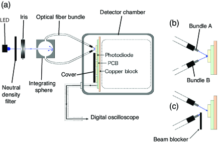
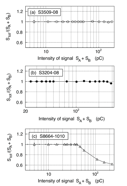
The signal linearity responses of the three photodiode and transimpedance preamplifier combinations were measured [38, 39] using the setup of Fig. 5(a). A light emitting diode (Thorlabs M450D3) produced a 100 ns long light pulse of emission wavelength nm, power mW, and emission angle . The light was attenuated using a pair of variable neutral density filter wheels and an iris, before being coupled into a 51 mm diameter integrating sphere (Thorlabs IS200) that had an internal surface reflectivity of 99%. The propagation direction and polarization of the light was thus randomized. Part of this light was extracted from the sphere through a pair of optical fiber bundles (Thorlabs BF20HSMA01) that each consisted of 7 multimode optical fibers of core diameter m and numerical aperture . The fibers were made of fused silica with a high concentration of hydroxyl groups (OH). The intensity of the light emitted from each fiber bundle [indicated by A and B in Fig. 5(b)] was found to be equal to within . The light was expanded using aspheric lenses of focal length mm (Thorlabs F280SMA-A) into a 8 mm diameter spot on the surface of one of the photodiodes. The other four photodiodes in the array were masked with a sheet of black rubber. The APD’s were biased at the nominal voltage V. Measurements were carried out by irradiating the photodiode with, a): only the light beam emitted from bundle A [see Fig. 5(c)] corresponding to a measured signal intensity at the output of the readout circuit of Fig. 2, b): the light from bundle B corresponding to an intensity , and c): simultaneous irradiation by the two beams corresponding to a measured signal intensity [Fig. 5(b)]. Any saturation in the photodiode or preamplifier would lead to the value being smaller than the expected sum . In Fig. 6 the measured fraction at various sums of the driver amplifier output (Fig. 2) in pC are shown for each photodiode type. Both p-i-n photodiode-amplifier combinations remained linear up to pC. Any residual nonlinearity is primarily caused by the transimpedance and buffer amplifiers. The APD’s on the other hand saturated at a signal output of pC, presumably due to space-charge effects in the depletion region of the APD reducing the effective gain.
3 Measurements
3.1 Relative light yields of Cherenkov radiators
The schematic layout of the experimental setup used to measure the relative light yields of the Cherenkov radiators against antiproton annihilations are shown in Fig. 7 [36, 37]. The AD provided a 200 ns long pulsed beam containing antiprotons with a kinetic energy MeV and repetition rate Hz. The beam was transported along an evacuated beamline. About 25% of the beam was decelerated to keV by allowing the antiprotons to pass through a radiofrequency quadrupole decelerator (RFQD). A momentum analyzer beamline selected the keV antiprotons and transported them to a cryogenic target chamber filled with helium gas. The antiprotons came to rest in the helium or metallic walls of the target chamber and underwent nuclear absorption and annihilation. Past experiments show (see Ref. [7] and references therein) that on average some 1.5 mesons, 1.8 mesons, and 2 mesons emerge from a +4He annihilation, and that the momentum of most of the pions are distributed between and 0.9 GeV/c. The mesons preferentially decay into two rays while still inside the target. The annihilations also lead to fission of the target nuclei, and the emission of fast and slow neutrons.
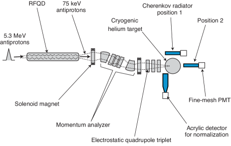
A single -PbF2 crystal was oriented so that either its short (indicated by position 1 in Fig. 7) or long (position 2) axis aligned towards the center of the experimental target at a distance mm. The Cherenkov light produced in the crystal by the antiproton annihilations were measured by a fine-mesh photomultiplier tube (Hamamatsu Photonics R5505G-ASSY) [7] with a bialkali photocathode of diameter mm and an entrance window made of borosilicate glass. The photomultiplier had a quantum efficiency of at wavelengths –440 nm. The measurements were repeated for the fused silica, acrylic, lead glass, and S-TIH53W glass radiators, and a plastic scintillator (Eljen EJ-200) of the same size. The photon yields at position 1 were measured with and without a transparent mm thick disk made of a two-component silicone rubber (Shinetsu Silicone CAT-103 and KE-103) inserted between the radiator and the entrance window of the photomultiplier to improve the optical coupling. The relative intensity of each antiproton pulse was normalized using the readout of a second Cherenkov detector of size 480 mm160 mm20 mm made of UV-transparent acrylic (Mitsubishi Rayon, Acrylite000). The detector was positioned 400 mm away from the target, so that the solid angle seen from the target was .
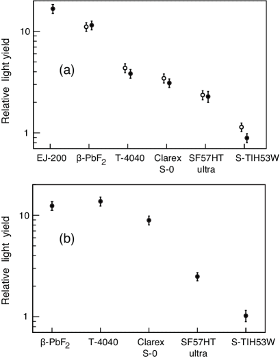
The relative light yields of the five radiators and plastic scintillator measured at position 1 are compared in Fig. 8(a). Each data point represents the average of measurements collected over 30 antiproton pulses, using three samples of each radiator type. The -PbF2 crystals showed the highest light yield that was a factor three larger than the values of the fused silica and acrylic radiators. This is due to the short radiation length and high refractive index of -PbF2 that allowed the efficient detection of -rays and low-momentum pions. Primarily because of the low transparencies at short wavelengths, the lead glass and S-TIH53W radiators showed light yields that were factors of 5 and 10 smaller compared to -PbF2, respectively. No significant differences were seen between the -values measured with (indicated by open circles) and without (filled circles) the silicone light coupler placed between the radiators and photomultiplier.
Fig. 8(b) shows the light yields measured with the five radiator types placed at position 2. The -values of the fused silica and -PbF2 radiators are now approximately equal, despite the factor shorter radiation length of the latter material. This is believed to be due to the lower transparency of -PbF2 compared to fused silica which results in the absorption of a significant number of those UV Cherenkov photons that were produced in the part of the crystal closest to the experimental target, that prevent them from reaching the photomultiplier.
3.2 Nuclear counter effects
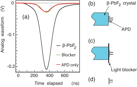
We next studied the nuclear counter effect (NCE) caused by secondary particles traversing the readout photodiodes. For this the -PbF2 array of Fig. 1 was positioned at a distance mm from the cryogenic helium target, with the short axis of the crystals aligned towards the direction where the antiprotons annihilated. The AD provided a 400 ns long antiproton beam. The black curve of Fig. 9(a) shows the analog waveform of the signal obtained by reading out the -PbF2 crystals using APD’s, and averaging the data accumulated over 10 consecutive arrivals of antiproton pulses at the target. A schematic drawing of one of the five crystal-APD connections in the array is shown in Fig. 9(b). The APD’s were biased at a voltage V. The signal is a superposition of the flash of Cherenkov light in the crystal and the NCE, and shows the temporal profile of the beam. To roughly estimate the contribution of the NCE, the measurement was repeated with a black rubber sheet placed between the crystals and the APD’s to prevent the Cherenkov photons from reaching the APD’s [Fig. 9(c)]. The measured waveform [indicated by the green curve of Fig. 9(a)] shows that of the detector signal arises from the NCE. The measurement was repeated with the -PbF2 crystals removed from the detector. No significant change [red curve of Fig. 9(a)] was seen compared to the measurement with the rubber sheet. This indicates that the effect of the crystals shielding the APD’s from secondary particle hits was relatively small under the geometric layout of the experiment.
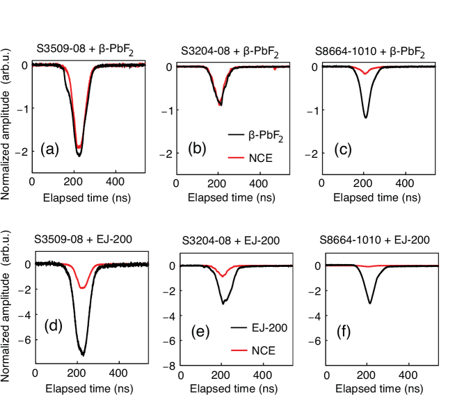
We next repeated the measurements by using the S3509-08 and S3204-08 p-i-n photodiodes as well as the APD’s to read out the five -PbF2 crystals. The resulting waveforms are shown using black curves in Figs. 10(a)–(c). The pulse duration of the antiproton beam was reduced to ns during these measurements. Each waveform represents the average of data collected from five antiproton pulses. The signal was normalized against the intensity of the antiproton beam which was measured using a separate acrylic Cherenkov detector read out by a fine-mesh photomultiplier tube. The NCE waveforms of each photodiode type measured by removing the -PbF2 crystals are shown superimposed using red curves. The fact that the amplitudes of the p-i-n photodiode waveforms measured with and without the crystals are similar shows that most of the detector signal arises from the NCE. This agrees with the results of Monte-Carlo simulations [40] that indicate that each pion hit on a p-i-n photodiode predominantly produced ion-electron pairs, compared to an estimated few hundred photoelectrons collected per hit on the Cherenkov radiator. The amplitude of the NCE waveform was proportional to the number of antiproton annihilations. The NCE effectively restricted the sensitive volume of the detector against charged pion and -ray hits to the –0.5 cm3 depletion regions in the photodiodes, instead of the full 720 cm3 volume of the -PbF2 crystal array. The measurements of the antiproton annihilations were repeated using the EJ-200 plastic scintillator array. The signal waveforms of the scintillators read out by the three types of photodiodes are plotted in Figs. 10(d)–(f) using black curves. In the case of the p-i-n photodiode, the NCE contribution [red curves of Figs. 10(d)–(e)] corresponded to of the total signal.
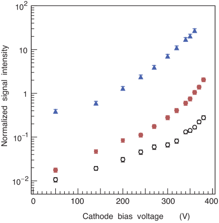
Fig. 11 shows the relative intensities of the APD signals against antiproton annihilations, measured at bias voltages between V and 400 V. Each data point corresponds to the average of data collected from five antiproton pulses, which were normalized against the intensity of the antiproton beam measured using the acrylic Cherenkov detector. Measurements were carried out with (indicated by closed circles) and without (open circles) a -PbF2 radiator crystal coupled to the APD. At low bias voltages V which corresponded to an APD gain near unity, the NCE constituted of the total signal. At higher bias V corresponding to a APD gain , the relative intensity of the NCE was reduced to of the Cherenkov detector signal as mentioned above. A similar tendency of smaller relative NCE at higher gain was seen for APD’s reading out plastic scintillators (indicated in Fig. 11 by triangles), though some saturation in the signal was seen at V. At a bias V, the NCE corresponded to of the total signal, as shown in the signal waveforms of Fig. 10(f).
3.3 Antiproton beam intensity
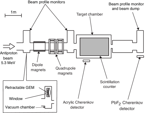
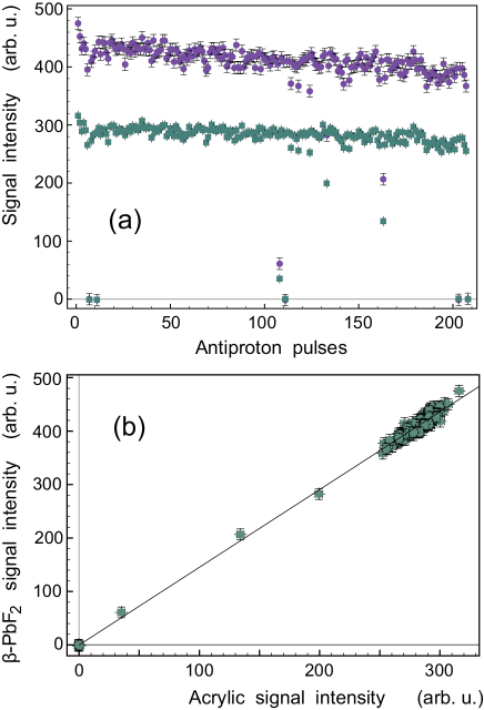
Fig. 12(a) shows the relative intensities of 205 antiproton pulses that were decelerated by the RFQD to energy keV over a 8 h period, measured using the -PbF2 Cherenkov detector array read out by APD’s (indicated by filled circles). A bias voltage V was used. We simultaneously measured the response of the acrylic Cherenkov detector read out by a fine-mesh photomultiplier (filled squares), which is known to be highly linear at these beam intensities [7]. The shot-to-shot fluctuations seen here were primarily caused by variations in the number of antiprotons that were created in the production target of the AD. The correlation between the intensity measurements made by the two detectors [Fig. 12(b)] indicates that the linearity of the -PbF2 Cherenkov detector array is better than . The residual nonlinearity is assumed to be mostly due to the contribution of the NCE and the response of the APD at high light intensities. Time- and temperature-dependent shifts in the APD gain were estimated to be of order .
Fig. 13 shows the layout of an experiment [3] employing the -PbF2 Cherenkov detector, in which the total cross section of antiprotons with kinetic energy MeV annihilating in a carbon target was measured. In the experiment, radiofrequency cavities were first used to bunch the antiprotons circulating in the AD into six pulses which were distributed equidistantly around its 190 m-circumference. These pulses of length ns were then sequentially extracted to the experiment at intervals of s, by exciting a kicker magnet located within the AD. The beam was focused by a quadrupole doublet before entering a 3-m long vacuum chamber containing a diamond-like carbon target with a thickness of either or . Between 1 and 10 annihilations occurred via in-flight nuclear reactions for every antiprotons traversing the target foil. The remaining antiprotons emerged from the other side of the foil, traversed a 2 m long section of evacuated beam pipe, and stuck a profile monitor based on gas electron multipliers (GEMs) located at the end of the experiment. This GEM detector was mounted inside the vacuum pipe of the beamline, and functioned as a beam dump where all the antiprotons annihilated. The -PbF2 Cherenkov detector was positioned 300 mm away from the GEM detector, with the short axis of the crystals aligned toward the annihilation position of the antiprotons. The relative intensity of the antiproton beam measured by the -PbF2 detector was used to appropriately normalize the annihilation counts measured by the scintillation counter to obtain the cross section. Further details and the results of the experiment are provided in Ref. [3].
4 Discussions and Conclusions
In conclusion, we have constructed a Cherenkov detector consisting of an array of five -PbF2 crystals of size 30 mm 30 mm160 mm read out by APD’s. The detector was used to measure the flux of secondary particles (mostly charged pions and rays) emerging from the annihilations of high-intensity antiproton beams. When the radiators were positioned so that the majority of the secondary particles entered the radiator in the direction parallel to its short axis, the light yield of the -PbF2 crystals measured with a bialkali photomultiplier tube was a factor –3 higher compared to acrylic and glass radiators of the same size. When the secondary particles traversed the long axis of the radiators, however, the light yields of the -PbF2 and fused silica radiators became approximately equal. This is presumably caused by the lower UV transmission of -PbF2 compared to fused silica. Cherenkov radiators read out using p-i-n photodiodes showed output signals that mostly consisted of the contribution from the nuclear counter effect (NCE) of secondary particles striking the photodiodes. APD’s were less affected by the NCE, so that its contribution in the case of -PbF2 readout was of the total signal in the experimental setup used by us. The p-i-n photodiode and APD readout of plastic scintillators showed that the NCE contribution was and for the two photodiode cases, respectively. We used the -PbF2 Cherenkov radiators read out by APD’s in a recent measurement to determine the cross section of antiprotons with kinetic energy MeV annihilating in carbon targets.
The authors are grateful to the ASACUSA collaboration and the proton synchrotron and Antiproton Decelerator operation teams of CERN. This work was supported by the Max-Planck-Gesellschaft.
References
References
- [1] A. Bianconi et al., Measurement of the antiproton-nucleus annihilation cross section at 5.3 MeV, Phys. Lett. B 704 (2011) 461.
- [2] M. Corradini et al., Experimental apparatus for annihilation cross-section measurements of low energy antiprotons, Nucl. Instrum. Meth. A 711 (2013) 12.
- [3] H. Aghai-Khozani et al., Measurement of the antiproton–nucleus annihilation cross-section at low energy, Nucl. Phys. A 970 (2018) 366.
- [4] H. Aghai-Khozani et al., First experimental detection of antiproton in-flight annihilation on nuclei at 130 keV, Eur. Phys. J. Plus 127 (2012) 125.
- [5] A. Sótér et al., Segmented scintillation detectors with silicon photomultiplier readout for measuring antiproton annihilations, Rev. Sci. Instrum. 85 (2014) 023302.
- [6] K. Todoroki et al., Instrumentation for measurement of in-flight annihilations of 130 keV antiprotons on thin target foils, Nucl. Instrum. Meth. A 835 (2016) 110.
- [7] M. Hori, K. Yamashita, R.S. Hayano, T. Yamazaki, Analog Cherenkov detectors used in laser spectroscopy experiments on antiprotonic helium, Nucl. Instrum. Meth. A 496 (2003) 102.
- [8] D.F. Anderson et al., Lead fluoride: An ultra-compact Cherenkov radiator for em calorimetry, Nucl. Instrum. Meth. A 290 (1990) 385.
- [9] C.L. Woody et al., A study on the use of lead fluoride for electromagnetic calorimetry, IEEE Trans. Nucl. Science 40 (1993) 546.
- [10] R.D. Appuhn et al., Electromagnetic calorimetry with lead fluoride crystals, Nucl. Instrum. Meth. A 350 (1994) 208.
- [11] P. Achenbach et al., Measurements and simulations of Cherenkov light in lead fluoride crystals, Nucl. Instrum. Meth. A 465 (2001) 318.
- [12] Th. Kirn et al., Properties of the most recent Hamamatsu avalanche photodiode, Nucl. Instrum. Meth. A 387 (1997) 199.
- [13] R. Lecomte et al., Radiation detection measurements with a new “buried junction” silicon avalanche photodiode, Nucl. Instrum. Meth. A 423 (1999) 92.
- [14] K. Dieters et al., Properties of the most recent avalanche photodiodes for the CMS electromagnetic calorimeter, Nucl. Instrum. Meth. A 442 (2000) 193.
- [15] J. Kataoka et al., Recent progress of avalanche photodiodes in high-resolution X-rays and -rays detection, Nucl. Instrum. Meth. A 541 (2005) 398.
- [16] T. Ikagawa et al., Study of large area Hamamatsu avalanche photodiode in a -ray scintillation detector, Nucl. Instrum. Meth. A 538 (2005) 640.
- [17] M. Hori, J. Walz, Physics at CERN’s Antiproton Decelerator, Prog. Part. Nucl. Phys. 72 (2013) 206.
- [18] M. Hori, A. Sótér, V.I. Korobov, Proposed method for laser spectroscopy of pionic helium atoms to determine the charged-pion mass, Phys. Rev. A 89 (2014) 042515.
- [19] Y. Hosono, Sjafruddin, T. Iguchi, M. Nakazawa, Fast neutron detector using PIN-type silicon photodiode, Nucl. Instrum. Meth. A 361 (1995) 554.
- [20] A. Satpathy et al., Nuclear counter effect of silicon PIN photodiode used in CsI(Tl) calorimeter, Nucl. Instrum. Meth. A 391 (1997) 423.
- [21] R. Mao, L. Zhang, R-Y. Zhu, LSO/LYSO crystals for future HEP experiments, J. Phys.: Conf. Ser. 293 (2011) 012004.
- [22] S. Baunack et al., Measurement of strange quark contributions to the vector form factors of the proton at (GeV/)2, Phys. Rev. Lett. 102 (2009) 151803.
- [23] A.T. Fienberg et al., Studies of an array of PbF2 Cherenkov crystals with large-area SiPM readout, Nucl. Instrum. Meth. A 783 (2015) 12.
- [24] J. Kaspar et al., Design and performance of SiPM-based readout of PbF2 crystals for high-rate, precision timing applications, JINST 12 (2017) P01009.
- [25] D.B. Cassidy, A.P. Mills Jr., A fast detector for single-shot positron annihilation lifetime spectroscopy, Nucl. Instrum. Meth. A 580 (2007) 1338.
- [26] M. Kobayashi et al., A new heavy and radiation-hard Cherenkov radiator based on PbWO4, Nucl. Instrum. Meth. A 459 (2001) 482.
- [27] P. Achenbach, Observation of scattering and absorption centers in lead fluoride crystals, IEEE Trans. Nucl. Science 48 (2001) 144.
- [28] G. Ren, D. Shen, S. Wang, and Z. Yin, Structural defects and characteristics of lead fluoride (PbF2) crystals grown by non-vacuum Bridgman method, J. Crystal Growth 243 (2002) 539.
- [29] G. Ren, D. Qun, Z. Li, and D. Shen, Transmission loss of lead fluoride crystals induced by oxygen contamination, J. Crystal Growth 247 (2003) 141.
- [30] Y. Jin et al., Study of a pure CsI crystal readout by APD for Belle II end cap ECL upgrade, Nucl. Instrum. Meth. A 824 (2016) 691.
- [31] Y. Kuno (COMET Collaboration), A search for muon-to-electron conversion at J-PARC: the COMET experiment, Prog. Theor. Exp. Phys. 2013 (2013) 022C01.
- [32] H. Ikeda et al., A detailed test of the CsI(Tl) calorimeter for BELLE with photon beams of energy between 20 MeV and 5.4 GeV, Nucl. Instrum. Meth. A 441 (2000) 401.
- [33] D.V. Dementyev et al., CsI(Tl) photon detector with PIN photodiode readout for a Kμ3 T-violation experiment, Nucl. Instrum. Meth. A 440 (2000) 151.
- [34] B. Aubert et al., The BABAR detector, Nucl. Instrum. Meth. A 479 (2002) 1.
- [35] M. Ablikim et al., Design and construction of the BESIII detector, Nucl. Instrum. Meth. A 614 (2010) 345.
- [36] M. Hori et al., Two-photon laser spectroscopy of antiprotonic helium and the antiproton-to-electron mass ratio, Nature 475 (2011) 484.
- [37] M. Hori et al., Buffer-gas cooling of antiprotonic helium to 1.5 to 1.7 K, and antiproton-to–electron mass ratio, Science 354 (2016) 610.
- [38] W. Budde, Multidecade linearity measurements on Si photodiodes, Appl. Opt. 18 (1979) 1555.
- [39] K.D. Mielenz and K.L. Eckerle, Spectrophotometer linearity testing using the double-aperture method, Appl. Opt. 11 (1972) 2294.
- [40] S. Agostinelli et al., Geant4 – a simulation toolkit, Nucl. Instrum. Meth. A 506 (2003) 250.