Fermi surface reconstruction and electron dynamics at the charge-density-wave transition in TiSe2
Abstract
The evolution of the charge carrier concentrations and mobilities are examined across the charge-density-wave (CDW) transition in TiSe2. Combined quantum oscillation and magnetotransport measurements show that a small electron pocket dominates the electronic properties at low temperatures while an electron and hole pocket contribute at room temperature. At the CDW transition, an abrupt Fermi surface reconstruction and a minimum in the electron and hole mobilities are extracted from two-band and Kohler analysis of magnetotransport measurements. The minimum in the mobilities is associated with the overseen role of scattering from the softening CDW mode. With the carrier concentrations and dynamics dominated by the CDW and the associated bosonic mode, our results highlight TiSe2 as a prototypical system to study the Fermi surface reconstruction at a density-wave transition.
The electronic properties of transition metal dichalcogenides (TMDs) are of fundamental and practical interest. Many TMDs can be tuned between semimetallic, semiconducting, and insulating behaviour and thus allow to access a plethora of different electronic characteristics. In addition, ordered states, e.g. due to charge-density-wave (CDW) formation Wilson et al. (1975); Wilson and Yoffe (1969) or superconductivity Morosan et al. (2006); Kusmartseva et al. (2009) are present in many members of the family with open questions on the underlying mechanism. Many of these TMDs can be exfoliated to atomic monolayers providing new tuning parameters and novel physics through the reduced dimensionality Xi et al. (2015a, b); Singh et al. (2017).
TiSe2 is a prototypical material for strong electronic interactions driving the CDW formation via a condensation of excitons, i.e. pairs of electrons and holes Di Salvo et al. (1976); Wilson (1978). Experimental and theoretical work have confirmed the relevance of the excitonic mechanism Hellmann et al. (2012); Cercellier et al. (2007); Kogar et al. (2017) which is widely accepted to work in cooperation with strong electron-phonon coupling Hedayat et al. (2019); Porer et al. (2014); van Wezel et al. (2010).
Above the CDW transition temperature , TiSe2 is characterised by small carrier concentrations stemming from up to three selenium-derived hole-like bands with cylindrical topology at the -point and a titanium-derived electron band with distorted and tilted ellipsoid topology present with 3-fold multiplicity at the L-point Bianco et al. (2015); Rasch et al. (2008); Watson et al. (2019a); Pillo et al. (2000) 111We use the high-temperature notation of the Brilluoin zone throughout the manuscript. In the low-temperature phase the high-temperature L-point folds back onto the high-temperature -point. Whether these bands overlap in energy or have a band gap remains uncertain. Either way, the overlap or gap is small or comparable to thermal energies down to .
Below the CDW transition temperature, the electronic structure of TiSe2 is dominated by a small electron pocket as shown by ARPES measurements Watson et al. (2019a). Knowledge of how the electronic structure and electron dynamics evolve upon thermally melting the CDW in equilibrium, however, are outstanding. Several studies suggested that the Fermi surface reconstruction from the CDW order and scattering associated with the CDW mode has a negligible effect on the electronic structure and dynamics Di Salvo et al. (1976); Watson et al. (2019b); Pillo et al. (2000); Monney et al. (2010a). Rather a dominance of thermal occupation effects was suggested. In the past, studies of the charge carrier concentration were based on a single-band analysis of Hall effect and optical reflectivity measurements despite the evidence for two bands being present while no measurements distinguishing the electron and hole dynamics across have been reported Velebit et al. (2016); Li et al. (2007). Here, we use high-resolution magnetotransport and quantum oscillation (QO) measurements to extract the temperature dependence of the charge carrier concentration and mobility of the electron and hole band. We directly observe one quasi-ellipsoid Fermi surface at low temperatures which is identified as an electron pocket. This electron pocket and a hole pocket grow rapidly above showing evidence of an abrupt Fermi surface reconstruction and gapping of of the charge carrier concentration in the CDW state. At the same time, we observe a minimum in the mobility on both the electron and hole pocket at highlighting the importance of scattering from the CDW forming phononic and/or electronic modes.
Single crystals of TiSe2 were grown by chemical vapour transport at as detailed in sec. SI of the Supplemental Material, and show a CDW transition at consistent with other studies of high-quality samplesTaguchi et al. (1981); Huang et al. (2017); Moya et al. (2019); Di Salvo et al. (1976); Hildebrand et al. (2014).
The low-temperature electronic structure of our TiSe2 samples is dominated by an electron pocket as evident from the combination of quantum oscillation measurements and magnetotransport. The QO data shown in Fig. 1 reveal a single frequency for magnetic fields parallel to the crystallographic direction, i.e. an orbit parallel to the basal plane. The increase of this frequency for orbits out of plane is well fitted by an ellipsoid shape (see Fig. 1(d) and S III of the Supplemental Material). This pocket is naturally associated with the L-point electron pocket observed by ARPES studies Watson et al. (2019a).
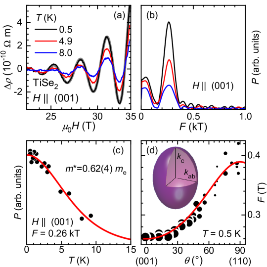
Magnetotransport measurements confirm the electron-dominated character of our samples at low temperature as can be seen from the negative Hall resistivity in Fig.2(a). Consistent with earlier reports Di Salvo et al. (1976); Campbell et al. (2019), changes sign smoothly around (cf. Fig. S2 of the Supplemental Material). The magnetoresistivity shown in Fig. 2(b-e) is small and positive. We use a two-band model with one electron and one hole band to simultaneously fit and as described in section S II of the Supplemental Material. The two-band fits shown as solid lines in Fig. 2 describe the data very well over the full temperature range.
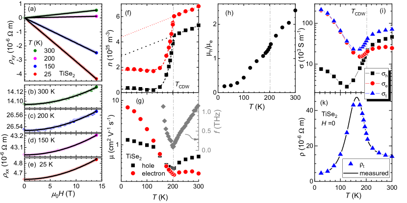
The charge carrier concentrations , and mobilities , for the electron and hole band respectively are shown in Fig. 2 (f) and (g). The low-temperature value of is in good agreement with our QO data and previous ARPES as well as heat capacity studies as summarised in Tab. S1 of the supplementary information. Thus the association of the observed QO frequency with the electron pocket is confirmed. The electron pocket observed in our QO measurements accounts for virtually the full low-temperature electronic heat capacity (cf. Tab. S1) highlighting the dominance of the electron pocket at low . The hole concentration extracted within the two-band model is very small at lowest temperatures and is likely to correspond to impurity states as indicated by the low hole mobility. We note that a free-electron single-band model cannot describe the low-temperature magnetotransport. Most notably, the Hall coefficient measured at lowest temperatures does not match with a free electron estimate for the electron pocket based on the QO results of .
At room temperature the electron and hole concentrations and are comparable in magnitude (cf. Fig. 2(f)). Above , and are associated with the 3D-like electron pocket at the L point and the 2D-like hole pocket at the point as seen by ARPES studies Rasch et al. (2008); Watson et al. (2019a). The small linear temperature dependence of and above (dotted lines in Fig. 2(f)) is attributed to the varying thermal occupation of the two bands similar to the model of Watson et al. Watson et al. (2019b). The slope of and at suggests a mass comparable to the free-electron mass for the electron band. The linear behaviour at high temperatures extrapolates to finite intercepts for both bands - these finite intercepts suggest a band overlap, i.e. not a gap, in the high-temperature phase above .
The charge carrier concentrations show a sharp drop below and saturate below . The drop is associated with condensation of electrons and holes into the CDW pair state and consequently with a Fermi surface reconstruction. The difference marks the loss of charge carriers and thus the density of electron-hole pairs. For , and can be described by activated behaviour as shown by dashed lines in Fig. 2(f).Fits of exponential form yield a gap , an energy scale consistent with . The fact, that the exponential form fits the data even close to suggests a finite gap up to . A finite gap at has indeed been seen in ARPES studies Chen et al. (2016); Mottas et al. (2019); Monney et al. (2010b) where the total gap is a sum of a BCS-like temperature dependent gap with an onset at on top of a weakly temperature dependent offset . Our exponential fits are dominated by the temperature dependence of just below where . The exponential form of and up to and the good agreement of the gap value with suggests a finite gap present above potentially due to fluctuating electron-hole pairs that condense at consistent with ARPES studies finding small intensity from backfolded bands above Cercellier et al. (2007).
The Fermi-surface reconstruction is further supported by the Kohler analysis Pippard (1989) presented in Fig. 3. The magnetoresistance follows a quadratic field dependence at . However, the quadratic coefficient (Kohler slope) shows a pronounced temperature dependence (cf. Fig. 3(b)). Above , is virtually constant and accordingly curves of MR vs collapse in Fig. 3(a). Below , however, rises very abruptly by more than an order of magnitude, passes a maximum at and saturates at a low-temperature value about double the room temperature value.
Kohler scaling and violations thereof have been observed in other CDW systems: In VSe2 and NbSe2, separate Kohler scaling is present below and above with a small difference in slope at Xue et al. (2020); Noto et al. (1980). In Ta2NiSe7 and NbSe3, Kohler scaling is only obeyed above . In underdoped cuprate superconductors, Kohler scaling is observed at low temperature throughout Chan et al. (2014). Our results on TiSe2 show a larger change in compared to other compounds because a larger fraction of the Fermi surface is affected by the CDW.
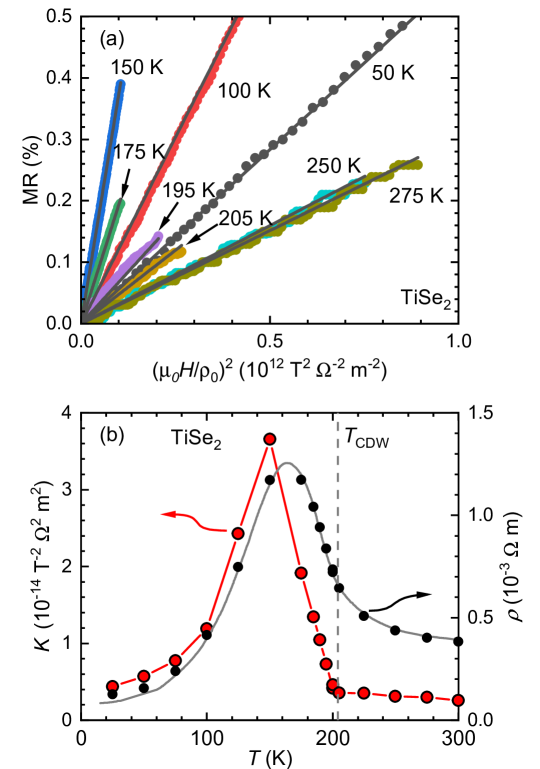
Our data suggest the Fermi surface reconstruction is the main reason for the violation of Kohler scaling in TiSe2. The sharp rise and strong temperature dependence of below can be due to (i) a reconstruction of the Fermi surface, (ii) an abrupt change in the anisotropy of the scattering time on the individual bands, or (iii) an abrupt change in the ratio of the scattering times of the electron and hole band, or a combination of the three. (iii) can be ruled out as this would manifest as an abrupt change of which is not observed (Fig. 2(h)). (ii) may contribute to the change of but it is unlikely to be the primary cause. For the violation of Kohler’s law to be dominated by changes to scattering time anisotropy, a drastic and abrupt change to the phonon spectrum would be required. This is unlikely to occur independent of the Fermi surface reconstruction. A moderate change of the phonon spectrum may occur as a consequence of the Fermi surface reconstruction through the electron-phonon coupling. Thus, the sudden change of at is dominated by (i) a sudden reconstruction of the Fermi surface. This is in agreement with the sudden drop of the charge carrier concentrations (Fig. 2(f)).
The mobilities of the individual bands show very strong and non-trivial temperature dependencies Fig. 2(g). At room temperature, the hole mobility is larger than the electron mobility whilst this is reversed at lowest temperatures. Both mobilities have a minimum at naturally associated with strong scattering from the softening mode associated with the CDW formation. Indeed, the temperature dependence of the mobilities show a dip similar in shape to the energy dependence of the L-point phonon mode Holt et al. (2001) (reproduced in Fig. 2(g)).
As noticed by Velebit et al. Velebit et al. (2016), the mobilities of the two bands are roughly equal at as shown in Fig. 2(h). This equality highlights that scattering from the L-point mode is the dominant process as the phase space for scattering from the electron to the hole band involves the density of states in both bands and the electron-phonon coupling.
The temperature dependence of the separated electron () and hole () conductivity are presented in Fig. 2(i). They show a minimum around and , respectively. The total conductivity and the total resistivity are dominated by and in different temperature regimes. The comparison of the thus calculated and the measured in Fig. 2(i) highlights the accuracy of the parameters extracted from the two-band fits.
From the temperature dependencies of the individual and total conductivities we identify that (i) at high temperature holes dominate the total conductivity and (ii) the negative above is a consequence of the hole mobility increasing with temperature above . (iii) The peak in is dominated by the loss of a large portion of charge carrier concentration of both holes and electrons due to the CDW with (iv) the positive at low temperatures arising due to the large increase in electron mobility towards lowest temperatures. (v) At low temperatures electrons dominate the conductivity. In summary, we conclude that the magnetotransport is dominated by the opening of the CDW gap and the scattering from the underlying bosonic mode.
Despite the smooth evolution of the resistivity, the magnetotransport behaviour provides direct evidence for an underlying abrupt Fermi surface reconstruction both as a large drop of the charge carrier concentrations and a sudden violation of Kohler’s law below . The analysis shows the loss of both electrons and holes below highlighting the strong coupling between them. The fact that a large fraction of the charge carrier concentration is involved in the formation of the CDW enables a clear view at the electronic scattering associated with the L-point CDW mode. The minimum in the mobility at is a direct match to the softening of the L-point mode and thus confirms that the dynamics of the charge carriers are directly linked to the dynamics of the CDW mode. Importantly, our measurements show that the strong scattering of the CDW mode causes the intriguing negative at room temperature. This makes TiSe2 uniquely suitable to observe the strong coupling of the CDW mode to the electronic states. The scattering of electrons from the softening CDW mode is obscured in other prototypical CDW systems like NbSe2 or VSe2 where only small portions of the Fermi surface are matched by the ordering wave vector and only these “hot” parts experience strong scattering Rossnagel et al. (2001); Strocov et al. (2012). Thus, TiSe2 is a prototypical system to study the effects of a Fermi surface reconstruction arising from a charge-density wave. These results will be relevant to understand systems like cuprate and iron-pnictide superconductors Putzke et al. (2018); Watson et al. (2015).
Acknowledgements.
The authors thank Jasper van Wezel, Jans Henke, Antony Carrington, Martin Gradhand, Matthew Wattson, and Phil King for valuable discussion. The authors acknowledge support by the EPSRC under grants EP/N01085X/1, EP/N026691/1, EP/L015544/1, NS/A000060/1, support of the HFML-RU/NWO, member of the European Magnetic Field Laboratory (EMFL), and funding from the European Research Council (ERC) under the European Union’s Horizon 2020 research and innovation programme (Grant agreement No. 715262-HPSuper).The research data supporting this publication can be accessed through the University of Bristol data repository TiS .
References
- Wilson et al. (1975) J. A. Wilson, F. Di Salvo, and S. Mahajan, Adv. Phys. 24, 117 (1975).
- Wilson and Yoffe (1969) J. A. Wilson and A. Yoffe, Adv. Phys. 18, 193 (1969).
- Morosan et al. (2006) E. Morosan, H. W. Zandbergen, B. S. Dennis, J. W. G. Bos, Y. Onose, T. Klimczuk, A. P. Ramirez, N. P. Ong, and R. J. Cava, Nat. Phys. 2, 544 (2006).
- Kusmartseva et al. (2009) A. F. Kusmartseva, B. Sipos, H. Berger, L. Forró, and E. Tutiš, Phys. Rev. Lett. 103, 236401 (2009).
- Xi et al. (2015a) X. Xi, L. Zhao, Z. Wang, H. Berger, L. Forró, J. Shan, and K. F. Mak, Nature Nanotechnology 10, 765 (2015a).
- Xi et al. (2015b) X. Xi, Z. Wang, W. Zhao, J.-H. Park, K. T. Law, H. Berger, L. Forró, J. Shan, and K. F. Mak, Nature Physics 12, 139 (2015b).
- Singh et al. (2017) B. Singh, C.-H. Hsu, W.-F. Tsai, V. M. Pereira, and H. Lin, PRB 95, 245136 (2017).
- Di Salvo et al. (1976) F. Di Salvo, D. Moncton, and J. Waszczak, Phys. Rev. B 14, 4321 (1976).
- Wilson (1978) J. A. Wilson, Phys. Status Solidi 86, 11 (1978).
- Hellmann et al. (2012) S. Hellmann, T. Rohwer, M. Kalläne, K. Hanff, C. Sohrt, A. Stange, A. Carr, M. M. Murnane, H. C. Kapteyn, L. Kipp, et al., Nat. Commun. 3, 1069 (2012).
- Cercellier et al. (2007) H. Cercellier, C. Monney, F. Clerc, C. Battaglia, L. Despont, M. G. Garnier, H. Beck, P. Aebi, L. Patthey, H. Berger, et al., Phys. Rev. Lett. 99, 146403 (2007).
- Kogar et al. (2017) A. Kogar, M. S. Rak, S. Vig, A. A. Husain, F. Flicker, Y. I. Joe, L. Venema, G. J. MacDougall, T. C. Chiang, E. Fradkin, et al., Science 358, 1314 (2017).
- Hedayat et al. (2019) H. Hedayat, C. J. Sayers, D. Bugini, C. Dallera, D. Wolverson, T. Batten, S. Karbassi, S. Friedemann, G. Cerullo, J. van Wezel, et al., PRRESEARCH 1, 023029 (2019).
- Porer et al. (2014) M. Porer, U. Leierseder, J.-M. Ménard, H. Dachraoui, L. Mouchliadis, I. E. Perakis, U. Heinzmann, J. Demsar, K. Rossnagel, and R. Huber, Nat. Mater. 13, 857 (2014).
- van Wezel et al. (2010) J. van Wezel, P. Nahai-Williamson, and S. S. Saxena, Phys. Rev. B 81, 165109 (2010).
- Bianco et al. (2015) R. Bianco, M. Calandra, and F. Mauri, Phys. Rev. B 92, 094107 (2015).
- Rasch et al. (2008) J. C. E. Rasch, T. Stemmler, B. Müller, L. Dudy, and R. Manzke, Phys. Rev. Lett. 101, 237602 (2008).
- Watson et al. (2019a) M. D. Watson, O. J. Clark, F. Mazzola, I. Marković, V. Sunko, T. K. Kim, K. Rossnagel, and P. D. C. King, Phys. Rev. Lett. 122, 076404 (2019a).
- Pillo et al. (2000) T. Pillo, J. Hayoz, H. Berger, F. Lévy, L. Schlapbach, and P. Aebi, Phys. Rev. B 61, 16213 (2000).
- Note (1) Note1, we use the high-temperature notation of the Brilluoin zone throughout the manuscript. In the low-temperature phase the high-temperature L-point folds back onto the high-temperature -point.
- Watson et al. (2019b) M. D. Watson, A. M. Beales, and P. D. C. King, Phys. Rev. B 99, 195142 (2019b).
- Monney et al. (2010a) C. Monney, E. F. Schwier, M. G. Garnier, N. Mariotti, C. Didiot, H. Cercellier, J. Marcus, H. Berger, A. N. Titov, H. Beck, et al., New J. Phys. 12, 125019 (2010a).
- Velebit et al. (2016) K. Velebit, P. Popčević, I. Batistić, M. Eichler, H. Berger, L. Forró, M. Dressel, N. Barišić, and E. Tutiš, Phys. Rev. B 94, 075105 (2016).
- Li et al. (2007) G. Li, W. Hu, D. Qian, D. Hsieh, M. Hasan, E. Morosan, R. Cava, and N. Wang, Phys. Rev. Lett. 99, 027404 (2007).
- Taguchi et al. (1981) I. Taguchi, M. Asai, Y. Watanabe, and M. Oka, Physica B+C 105, 146 (1981).
- Huang et al. (2017) S. H. Huang, G. J. Shu, W. W. Pai, H. L. Liu, and F. C. Chou, Phys. Rev. B 95, 045310 (2017).
- Moya et al. (2019) J. M. Moya, C.-L. Huang, J. Choe, G. Costin, M. S. Foster, and E. Morosan, PRMATERIALS 3, 084005 (2019).
- Hildebrand et al. (2014) B. Hildebrand, C. Didiot, A. M. Novello, G. Monney, A. Scarfato, A. Ubaldini, H. Berger, D. R. Bowler, C. Renner, and P. Aebi, Phys. Rev. Lett. 112, 197001 (2014).
- Campbell et al. (2019) D. J. Campbell, C. Eckberg, P. Y. Zavalij, H.-H. Kung, E. Razzoli, M. Michiardi, C. Jozwiak, A. Bostwick, E. Rotenberg, A. Damascelli, et al., Phys. Rev. Materials 3, 053402 (2019).
- Holt et al. (2001) M. Holt, P. Zschack, H. Hong, M. Y. Chou, and T.-C. Chiang, Phys. Rev. Lett. 86, 3799 (2001).
- Chen et al. (2016) P. Chen, Y.-H. Chan, X.-Y. Fang, S.-K. Mo, Z. Hussain, A.-V. Fedorov, M. Y. Chou, and T.-C. Chiang, Scientific Reports 6, 37910 (2016).
- Mottas et al. (2019) M.-L. Mottas, T. Jaouen, B. Hildebrand, M. Rumo, F. Vanini, E. Razzoli, E. Giannini, C. Barreteau, D. R. Bowler, C. Monney, et al., PRB 99, 155103 (2019).
- Monney et al. (2010b) C. Monney, E. F. Schwier, M. G. Garnier, N. Mariotti, C. Didiot, H. Beck, P. Aebi, H. Cercellier, J. Marcus, C. Battaglia, et al., Phys. Rev. B 81, 155104 (2010b).
- Pippard (1989) B. Pippard, Magnetoresistance in metals (Cambridge University Press, 1989).
- Xue et al. (2020) Y. Xue, Y. Zhang, H. Wang, S. Lin, Y. Li, J.-Y. Dai, and S. P. Lau, Nanotechnology 31, 145712 (2020).
- Noto et al. (1980) K. Noto, S. Morohashi, K. Arikawa, and Y. Muto, Physica B+C 99, 204 (1980).
- Chan et al. (2014) M. K. Chan, M. J. Veit, C. J. Dorow, Y. Ge, Y. Li, W. Tabis, Y. Tang, X. Zhao, N. Barišić, and M. Greven, PRL 113, 177005 (2014).
- Rossnagel et al. (2001) K. Rossnagel, O. Seifarth, L. Kipp, M. Skibowski, D. Voß, P. Krüger, A. Mazur, and J. Pollmann, Phys. Rev. B 64, 235119 (2001).
- Strocov et al. (2012) V. N. Strocov, M. Shi, M. Kobayashi, C. Monney, X. Wang, J. Krempasky, T. Schmitt, L. Patthey, H. Berger, and P. Blaha, Phys. Rev. Lett. 109, 086401 (2012).
- Putzke et al. (2018) C. Putzke, J. Ayres, J. Buhot, S. Licciardello, N. E. Hussey, S. Friedemann, and A. Carrington, Phys. Rev. Lett. 120, 117002 (2018).
- Watson et al. (2015) M. D. Watson, T. Yamashita, S. Kasahara, W. Knafo, M. Nardone, J. Béard, F. Hardy, A. McCollam, A. Narayanan, S. F. Blake, et al., Phys. Rev. Lett. 115, 027006 (2015).
- (42) Doi: 10.5523/bris.xxx, Data repository at the University of Bristol, URL http://dx.doi.org/10.5523/bris.xxx.