Symmetry breaking and circular photogalvanic effect in epitaxial \ceCd_xHg_1-xTe films
Abstract
We report on the observation of symmetry breaking and the circular photogalvanic effect in \ceCd_xHg_1-xTe alloys. We demonstrate that irradiation of bulk epitaxial films with circularly polarized terahertz radiation leads to the circular photogalvanic effect (CPGE) yielding a photocurrent whose direction reverses upon switching the photon helicity. This effect is forbidden in bulk zinc-blende crystals by symmetry arguments, therefore, its observation indicates either the symmetry reduction of bulk material or that the photocurrent is excited in the topological surface states formed in a material with low Cadmium concentration. We show that the bulk states play a crucial role because the CPGE was also clearly detected in samples with non-inverted band structure. We suggest that strain is a reason of the symmetry reduction. We develop a theory of the CPGE showing that the photocurrent results from the quantum interference of different pathways contributing to the free-carrier absorption (Drude-like) of monochromatic radiation.
I Introduction
Cd_xHg_1-xTe alloy, also known as MCT (Mercury Cadmium Telluride), is one of the most leading materials used for sensitive and fast infrared detectors Capper (1997); Norton (2002); Henini and Razeghi (2002); Rogalski (2005); Downs and Vandervelde (2013); Rogalski (2018); Vanamala et al. (2019). Wide bandgap tunability of these materials allows radiation detection in an extremely wide frequency range, spanning from near- to mid-infrared wavelength. Furthermore, it has been used for the development of terahertz (THz) radiation detection, see e.g. Refs. Dvoretsky et al. (2010); Rumyantsev et al. (2017); Ruffenach et al. (2017); Yavorskiy et al. (2018); Bąk et al. (2018). The introduction of the concept of topological insulators (TIs) Moore (2010); Hasan and Kane (2010); Zhang et al. (2011) attracted great attention to novel aspects of \ceCd_xHg_1-xTe compounds as well as low dimensional quantum heterostructures based on these materials. The reason for that is the inverted band structure in HgTe and \ceCd_xHg_1-xTe with a Cadmium concentration not exceeding the critical value Berchenko and Pashkovskii (1976); Orlita et al. (2014); Malcolm and Nicol (2015); Teppe et al. (2016); Tomaka et al. (2017), which is a crucial condition for the formation of helical surface or edge states Zhang et al. (2011); Dyakonov and Khaetskii (1981); Tomaka et al. (2017); Marchewka et al. (2017); Minkov et al. (1996); Kane and Mele (2005); Bernevig et al. (2006); Hasan and Kane (2010); Zhang et al. (2011). In comparison to other materials with a non-trivial band structure, CdHgTe-based compounds seem to be more promising due to their very high carrier mobility and feasibility to suppress effects from three-dimensional carriers in the sample volume. This is also supported by the well developed technological process originally motivated by the fabrication of detectors which has been adapted for the growth of TI materials on demand. The observation of Kane fermions in bulk \ceCd_xHg_1-xTe crystals Orlita et al. (2014); Malcolm and Nicol (2015); Teppe et al. (2016), quantum spin Hall effect Bernevig et al. (2006); König et al. (2007); Nowack et al. (2013) and helical edge photocurrents in CdHgTe/HgTe/CdHgTe quantum wells Dantscher et al. (2017) as well as the demonstration of Dirac surface states in 3D TI made of strained HgTe Brüne et al. (2011); Shuvaev et al. (2012); Kozlov et al. (2014); Brüne et al. (2014); Dantscher et al. (2015), are some important achievements in the physics of topological insulators. In the case of bulk \ceCd_xHg_1-xTe crystals the formation of helical surface states becomes possible due to the fact that the proper choice of the amount of Cadmium in the alloy yields an inversion of the band ordering, see e.g. Orlita et al. (2014); Teppe et al. (2016); Rigaux (1980). Furthermore, in materials with low the band structure can be changed from normal to inverted band ordering simply by a variation of the temperature, Teppe et al. (2016). Such - and -driven band inversions give rise to a large variety of novel physical concepts including the Veselago lenses Betancur-Ocampo and Gupta (2017), development of long wavelength lasers with suppression of the Auger processes Morozov et al. (2017); Utochkin et al. (2019), etc.
In all publications discussing the band structure, transport phenomena, opto-electronic effects, and magneto-optical properties of \ceCd_xHg_1-xTe films the point group symmetry of the crystal is considered to be Td. This follows from the crystallographic structure of the system. Here, investigating terahertz radiation induced photogalvanic currents in \ceCd_xHg_1-xTe films with an inverted band structure we surprisingly observed a well pronounced circular photogalvanic effect (CPGE) Ivchenko (2005); Ganichev and Prettl (2005), whose prerequisite is gyrotropy. Consequently, by symmetry arguments it is forbidden in the non-gyrotropic Td group. Therefore, the CPGE observation indicates either (i) the symmetry reduction of the bulk material or (ii) excitation of the photocurrent in the topological surface states formed in the material with low Cadmium concentration. We performed a careful study of terahertz radiation induced CPGE in bulk \ceCd_xHg_1-xTe films with structure compositions similar to that in most of the previous studies of topological surface states in this material. We show that an attempt to ascribe the generation of the CPGE solely to the helical topological surface states fails, because pronounced CPGE is also detected in crystals with above the critical one, which, correspondently, are characterized by a normal band ordering. To explain the origin of the observed CPGE, we suggest that the studied epitaxial films are strained and the actual symmetry of the crystal is reduced. In strained zinc-blende-type crystals, CPGE may emerge Lyanda-Geller and Pikus (1989). We develop a microscopic theory of the CPGE for the Drude-like indirect optical transitions in bulk crystals induced by terahertz radiation, which describes well the experimental findings. We show that the radiation helicity sensitive photocurrent stems from the interference of virtual transitions via the conduction and valence bands contributing to the real optical transitions.
II Samples and methods
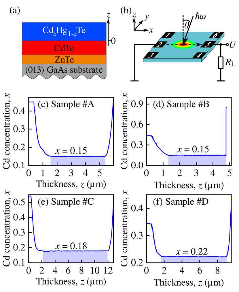
We studied \ceCd_xHg_1-xTe layers with graded band gap layers at absorber boundaries grown by molecular beam epitaxy on semi-insulating (013)-oriented \ceGaAs substrates. \ceZnTn ( thick) and \ceCdTe ( thick) buffer layers Sidorov et al. (2001) were fabricated on top of the \ceGaAs substrates. The structure composition is shown in Fig. 1 (a). The samples were quadratically shaped with approximate dimensions of , see Fig. 1 (b). Four samples with different profiles of the Cadmium concentration were prepared, see Fig. 1 (c)-(f). In three of these samples (#A,#C, and #D) the active layers with constant contents were sandwiched (surrounded) by regions with gradually growing Cadmium concentration. In sample #B, by contrast, the active layer was capped by \ceCd_0.85Hg_0.15Te. Note that due to the Fermi level position free carriers are located in the active layer and, in the films with in the topological surface states. The samples were supplied with several indium-soldered contacts bonded to a chip holder, see Fig. 1 (b).
As a radiation source for the photocurrent measurements two types of molecular gas THz lasers were used: On the one hand, a continuous wave () laser with a power of up to Olbrich et al. (2011), on the other hand a pulsed laser with a pulse duration of about , a repetition rate of and a peak power of up to Ganichev et al. (2002); Weber et al. (2008); Drexler et al. (2012). The lasers emitted frequency lines in the range between 0.6 and . The nearly gaussian-shaped beam, controlled by pyroelectric camera Ganichev (1999), was focused onto the sample using a parabolic mirror. The beam spot diameter varied, depending on the radiation frequency, from 1.5 to . The initially linearly polarized radiation was modified applying lambda-quarter plates made from crystal quartz. The rotation of these plates by the angle with respect to the initial laser polarization plane resulted in the controllable variation of the radiation polarization state. By that the degree of circular polarization was changed according to
| (1) |
where is the intensity of the right- (left-) handed circularly polarized radiation part. The Stokes parameters defining the degrees of linear polarization were varied according to Bel’kov et al. (2005)
| (2) |
THz radiation was applied at normal incidence or at oblique incidence with an angle of incidence . The photocurrent was measured as a voltage drop across a load resistor, see Fig. 1 (b), or as the voltage drop over the sample itself. The measurements were carried out in an optical cryostat which allowed us to access a temperature range from liquid helium to room temperature.
III Results
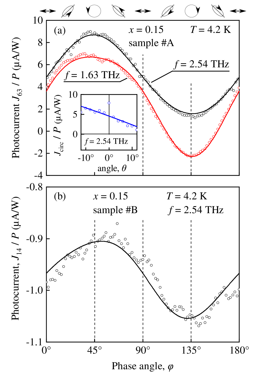
The circular photocurrent was first observed at liquid helium temperature in samples #A and #B with being characterized by the inverted band structure. Figure 2 shows the data obtained at normally incident radiation of low power radiation with frequencies 1.63 and . The overall polarization dependences can be well fitted by
| (3) |
In both samples the total photocurrent is dominated by the circular photocurrent described by the first term in Eq. (3) proportional to the coefficient , and the polarization independent offset, . Contributions proportional to the degrees of linear polarization, while being present, are substantially smaller. Generally, in non-centrosymmetric bulk \ceCd_xHg_1-xTe crystals polarization independent photocurrents as well as those proportional to the degree of linear polarization can stem from linear photogalvanic or photon drag effects Ivchenko (2005); Ganichev and Prettl (2005); Sturman and Fridkin (1992). These effects are well known for other non-centrosymmetric materials and are out of scope of our paper. By contrast, in such crystals the circular photocurrent is forbidden by symmetry arguments. Therefore, below we focus on the origin and properties of this photocurrent. Analyzing the circular photocurrent further we applied radiation at oblique incidence, see inset in Fig. 2 (a). This measurements demonstrated that the circular current varies with the angle of incidence as
| (4) |
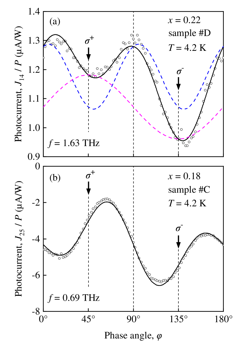
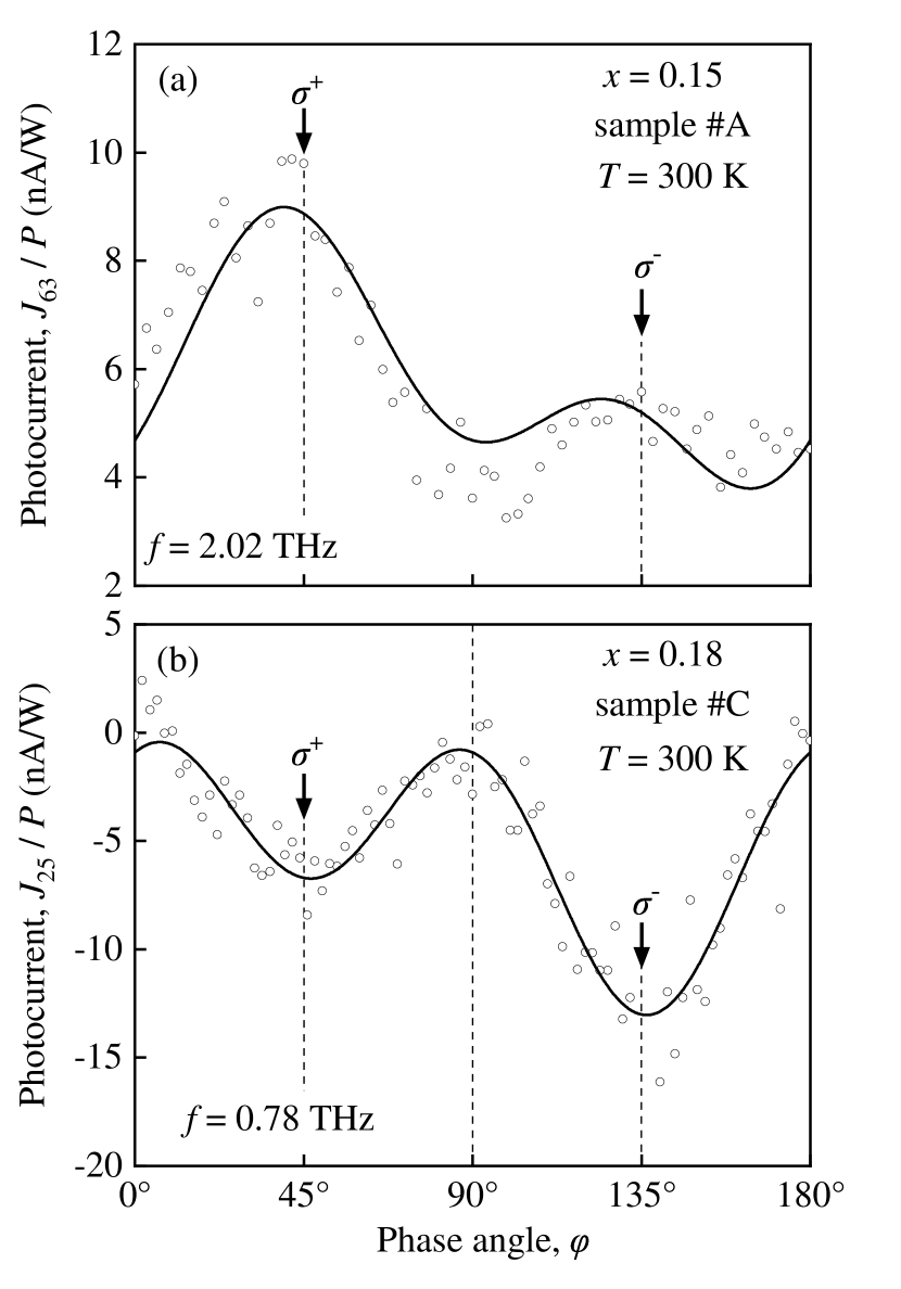
Samples #A and #B at liquid helium temperature have a \ceCd concentration in the active layer lower than the critical one and, therefore, are characterized by an inverted band ordering. The latter results in the formation of topological surface states. These states, at least for samples with an abrupt increase of the Cadmium concentration , like in the top layer of sample #B, are two-dimensional and, therefore, are characterized by reduced symmetry. Consequently, in such states the circular photogalvanic effect becomes possible. To prove that formation of the surface states is an unambiguous requirement for the generation of the circular photocurrent in the bulk \ceCd_xHg_1-xTe crystals we carried out measurements at liquid helium temperature in samples with normal band ordering (sample #D, active layer ) and with almost linear dispersion (sample #C, active layer with Cadmium concentration being close to the critical one). Figure 3 shows the data obtained applying normally incident radiation of a laser operating at frequencies 0.69, 1.63, and . In both cases the photocurrent can be well fitted by Eq. (3), surprisingly, with substantial contribution of the circular photocurrent. These results already rule out band inversion and topological states formation as a prerequisite of the CPGE in bulk \ceCd_xHg_1-xTe crystals. Moreover, applying the radiation of high power pulsed lasers, which increases the sensitivity of the method, we observed that the circular photocurrent can clearly be detected even at room temperature. This is shown in Fig. 4 for samples #A and #C with and . Previous studies of \ceCd_xHg_1-xTe crystals demonstrated that at room temperature all our samples are characterized by a normal band order and no topological states are present.
Summarizing the experimental part, our experiments provide clear evidence for the generation of the circular photogalvanic effect in bulk \ceCd_xHg_1-xTe crystals with both inverted and normal band orderings, as well as for samples with critical Cadmium concentration characterized by an almost linear energy dispersion. The fact that the CPGE is clearly detected for samples with larger than the critical one demonstrates that the CPGE generation is not limited to the films with topological surface states.
IV Theory and discussion
IV.1 Symmetry analysis
Bulk \ceCd_xHg_1-xTe has nominally zinc-blende crystal structure which is described by the point group. Despite the fact that the group lacks the center of space inversion, it is non-gyrotropic and does not support CPGE Ivchenko (2005). However, if the spatial symmetry of the crystal is reduced further, CPGE may emerge. The most likely origin of the symmetry reduction in our samples is strain stemming, e.g., from lattice mismatch at the \ceCd_xHg_1-xTe film interfaces. 111 Note that in samples with the CPGE caused by the optical transitions in the surface states may contribute to the total current. A similar current has been previously observed in HgTe 2D TIs Dantscher et al. (2017) and mechanisms are overviewed in Ref. Durnev and Tarasenko (2019) .
In strained zinc-blende crystals, CPGE can occur Lyanda-Geller and Pikus (1989). To first order in strain, the dependence of the CPGE current density on the static strain tensor is described by
| (5) |
where is the unit vector pointing along the photon wave vector , is the local intensity of radiation, and , , and are the cubic axes. The parameters and are linearly independent and describe the contributions to the photocurrent caused by normal and shear strain, respectively Lyanda-Geller and Pikus (1989). The CPGE current vanishes in the case of hydrostatic strain that does not disturb the crystal symmetry. Phenomenological Eqs. (5) can be readily constructed using the theory of group representations. In (013)-grown structures experimentally studied in our work, the tensor of strain induced by the lattice mismatch has four non-zero components , , , and in the coordinate frame , , and relevant to the structure orientation. Typically, the components and at the interfaces are determined by the lattice mismatch between the film and the buffer layer and are equal to each other. The other components, and , can be found by minimizing the elastic energy, see, e.g., Ref. Dantscher et al. (2015).
In the experiment on (013)-grown samples described above, we study the photocurrent excited by normally incident radiation (). For this geometry, and Eqs. (5) take the form
| (6) |
where is the angle between and , . A substantial photocurrent excited at normal incidence and sensitive to the degree of circular polarization has been detected in all samples for all frequencies and temperatures used, see Figs. 2-4 and in Eq. (4). This photocurrent corresponds to the in-plane component of photocurrent in Eq. (IV.1). Note that the geometry of the samples allows us to measure only the in-plane component of the current.
In addition to the helicity driven photocurrent at normal incidence experiment shows that tilting the light by an angle of incidence results in an additional photocurrent proportional to the degree of circular polarization being proportional to , see inset in Fig. 2(a). To describe the photocurrent at oblique incidence of radiation one should also take into account all components of . For in the coordinate frame Eqs. (5) transforms into
| (7) |
here describes position of the plane of incidence with respect to the crystallographic axes, which in the experiment is unknown. One can clearly see that even for arbitrary contributions of the photocurrent proportional to are present, which corresponds to in Eq. (4) describing experimental data in the inset in Fig. 2(a).
IV.2 Microscopic theory
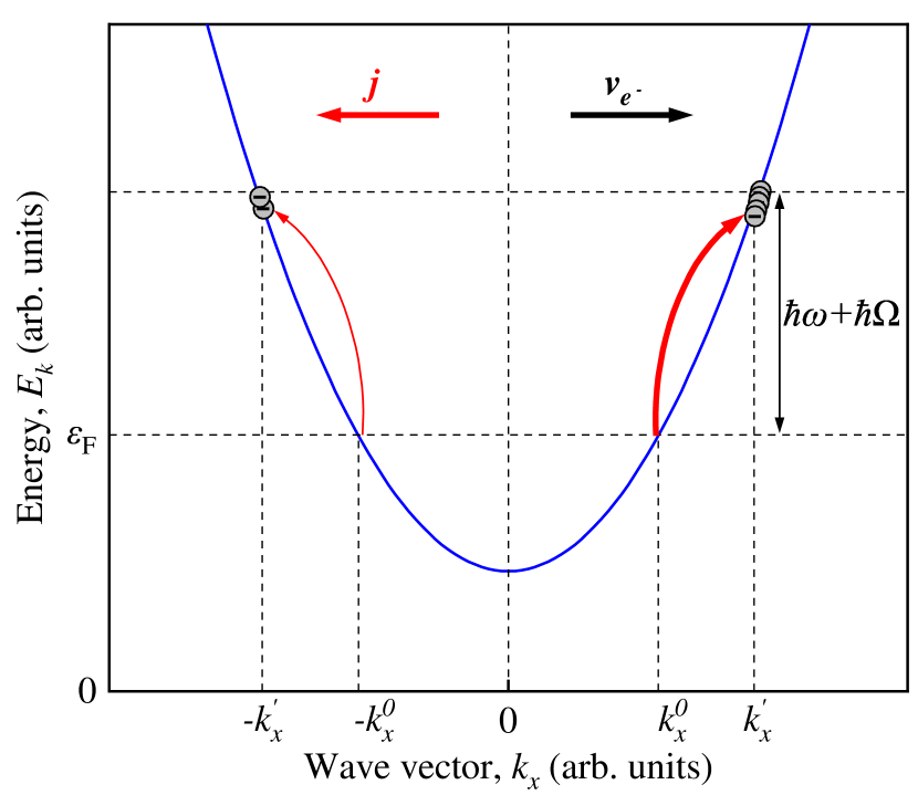
Now we turn to the microscopic mechanism of the photocurrent generation. We consider \ceCd_xHg_1-xTe with the content of Hg below the critical value of the transition to a 3D topological insulator. The samples have the conventional band structure with the conduction band and the valence band. The band gap is larger than the photon energy of THz radiation and free carriers are present in the sample. Therefore, the radiation is absorbed via indirect optical transitions (Drude-like) in the conduction band, see Fig. 5. These transitions are assisted by the scattering of electrons by phonons or static defects of the structure to simultaneously satisfy the laws of energy and quasi-momentum conservation. Indirect optical transitions are described by the second-order perturbation theory involving virtual processes via intermediate states. The matrix element of the real transition from the initial state , where is the wave vector and is the spin index, to the final state is given by the sum of the compound matrix elements of the virtual transitions via all possible intermediate states ,
| (8) |
where and are the matrix elements of the electron scattering and electron-phonon interaction, respectively, and is the total energy of the system in the state.
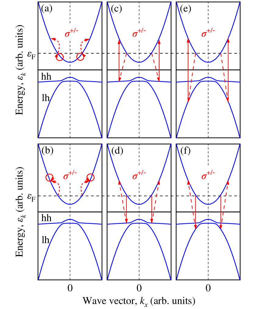
The main contribution to radiation absorption comes from the virtual transitions with intermediate states in the conduction band, Fig. 6. There are two types of such processes: the processes where electron-photon interaction is followed by electron scattering [shown in Fig. 6 (a)] and the processes with the opposite order [shown in Fig. 6 (b)]. The virtual transitions via the conduction-band states describe well the Drude absorption. However, they are not sensitive to the circular polarization of the radiation and do not introduce asymmetry in the electron distribution in the space.
To obtain the photocurrent, one should also take into account the virtual transitions with intermediate states in the valence band Tarasenko (2007). Figures 6 (c)-6 (f) sketch four possible processes of such type via the heavy-hole and the light-hole bands. Due to the selection rules for interband optical transitions, these processes are sensitive to the radiation helicity Ivchenko and Tarasenko (2004). Moreover, their contributions can be quite large because the band gap in \ceCdHgTe samples, and correspondingly the denominator in Eq. (8), is small.
The probability of the real transitions is determined by the squared modulus of the matrix element
| (9) |
where are the matrix elements of the virtual transitions via the band. It contains the interference term . The term does not vanish in non-centrosymmetric crystals and is responsible for the circular photogalvanic effect Tarasenko (2007).
The circular photocurrent emerges only in strained crystals. Therefore, in the calculation of the matrix elements of the virtual transitions we also take into account the mixing of the states by the static strain. Otherwise, the photocurrent vanishes in agreement with the symmetry analysis presented above. The strain-induced mixing of the heavy-hole and light-hole states is schematically shown in Fig. 6 as a distortion of the valence-band spectrum.
To summarize, the microscopic model takes into account two ingredients essential for the CPGE: (i) the lack of space inversion center in the crystal which enables the interference of the optical transition pathways via the conduction and valence bands and (ii) the strain-induced mixing of the states.
We calculate the photocurrent in the 6-band Kane model considering the static strain of the crystal and the electron scattering by acoustic phonons. In the basis of the and states, the Kane Hamiltonian has the form Bir and Pikus (1974)
| (10) |
where is the zero matrix, is the identity matrix,
| (11) |
and is the Kane parameter. The Hamiltonian (10) describes six eigenstates: the conduction-band states with the dispersion , the states in the light-hole subband with the dispersion , and the dispersionless states in the heavy-hole subband with the energy . Here, is the effective mass. The Hamiltonian of electron-photon interaction is given by
| (12) |
where is the electron charge, is the speed of light, is the vector potential of the electromagnetic field related to the radiation intensity by , and is the refractive index of the crystal. The strain Hamiltonian in the 6-band model is given by
| (13) |
where in the conduction-band deformation potential, is the strain tensor, is the Bir-Pikus Hamiltonian which, in the spherical approximation, has the form Bir and Pikus (1974)
| (14) |
and are the valence-band deformation potentials, are the matrices of the angular momentum , and is the part describing the strain-induced coupling of the and states in zinc-blende crystals Pikus et al. (1988); Ivchenko and Tarasenko (2004),
| (15) |
and is the interband deformation potential. The Hamiltonian (13) is used to calculate both the mixing of the states by the static strain and the electron scattering by longitudinal acoustic (LA) phonons. The tensor of strain produced by the LA phonons is given by
| (16) |
where is the phonon wave vector, is the crystal density, is the photon frequency, is the speed of longitudinal sound, and and are the operators of phonon annihilation and creation, respectively. We assume that the photon frequency considerably exceeds both the frequency of phonons involved in scattering and the scattering rate , and that the phonon occupation numbers are large, i.e., , where is the temperature. To the first order in the wave vector, the matrix elements of the virtual transitions via the conduction band with the absorption of a photon and the simultaneous emission () or absorption () of a LA phonon has the form
| (17) |
In calculating the matrix elements of the virtual transitions via the valence band we take into account the mixing of the heavy-hole and light-hole stated by the static strain. The corresponding contribution to proportional to the static strain can be obtained by the third-order perturbation theory and is given by
| (18) |
where the indexes and run over the valence subbands. The matrix elements of electron scattering with the emission or absorption of a LA phonon and the matrix elements of heavy-hole–light-hole mixing by the static strain are calculated using the strain Hamiltonian (13). The exact analytical expression for is too cumbersome to be printed. An estimation capturing the dependence on the band-structure parameters and deformation potentials is the following .
The photocurrent in the relaxation time approximation is given by the standard expression
| (19) |
where is the momentum relaxation time, is the electron velocity, and is the equilibrium Fermi-Dirac distribution function.
Labour-consuming calculation of Eq. (19) with the matrix elements (17) and (18) yields the CPGE current (5) with the coefficients
| (20) |
and . Now using Eq. (IV.1) one can already obtain the equation for the in-plane photocurrent which describes well all major experimental findings. To proceed further, we assume that the momentum relaxation of electrons is also determined by the electron-phonon interaction. For quasi-elastic scattering by LA phonons, the momentum relaxation time depends on energy and has the form
| (21) |
The relaxation time of the average electron velocity in the model of the drifting electron gas is given by
| (22) |
which gives
| (23) |
where
| (24) |
is the mean value of . Taking into account Eq. (23) and , we can rewrite Eq. (20) in the form
| (25) |
In the case when the photon energy is much less than the mean electron energy , Eq. (25) takes the form
| (26) |
where is the electron density.
Finally, the in-plane photocurrent induced at normal incidence of radiation in (013)-oriented films is given by
| (27) |
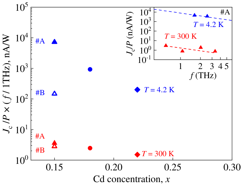
This equation describes the observed polarization dependence of the photocurrent, its almost linear increase with the frequency decrease as well as drastic increase of the photocurrent magnitude by cooling the sample from room to liquid helium temperature. Indeed, the proportionality of the photocurrent to the radiation helicity has already been addressed above and is clearly seen in Figs. 1-4 obtained for 4.2 and 300 K. The inset in Fig. 7 presenting the circular photocurrent as a function of the radiation frequency shows that it varies after , which agrees with Eq. 27. Results obtained for samples with different Cd contents and temperatures, are characterized by substantially different energy gaps. According to Eq. 27 the latter should strongly affect the circular photocurrent magnitude yielding drastic increase of the current amplitude upon the energy gap reduction (). Figure 7 and Tab. 1 present the magnitude of the circular photocurrent obtained for different samples and temperatures. Note that to make comparison of data obtained at different frequencies possible, we used the fact that and normalized the data to the radiation frequency. The figure reveals that at fixed temperature, either 300 K or 4.2 K, substantially reduces with the band gap increase, see Table 1. Furthermore, comparing the photocurrent magnitudes in each individual sample we see that the photocurrent is increased by more than two orders of magnitude at the temperature decrease from 300 to 4.2 K. This fact is in agreement with substantial reduction of the band gap at low temperatures. The values of for different sample compositions and temperatures are taken from Refs. Teppe et al. (2016); Rigaux (1980); Laurenti et al. (1990). We note that for samples #A and #B at , the band gap becomes negative and applicability of Eq. 27 is not justified. Now we estimate from the room temperature experiment the strain . Room temperature data are used because, under these conditions, all the samples have a normal band dispersion, thus no topologically protected surface states can be formed and this case is relevant to the above derived equation for the photocurrent. The current density was obtained from the photocurrent measured in experiment after , where is the width of the conducting channel, is the radiation beam diameter and is the beam area. Note that while for room temperature results this calculation seems to be reasonable at helium temperatures it is not straightforward, because free carriers and, consequently, the current may be distributed inhomogeneous across the sample. The latter unknown factor makes a quantitative comparison of data with the theory difficult. Table 1 presents the strain obtained using the parameters eV Novik et al. (2005), eV, and Adachi (2004). While the rate is unknown for HgTe, we use for GaAs Pikus et al. (1988). Table 1 shows that the strain in samples with different compositions varies from to and is well below the strain estimated by minimizing the elastic energy for pure HgTe () deposited on \ceCdTe substrate. Dantscher et al. (2015). We note that a small value of the strain is not surprising because we deal with thick films. Under this condition strain is expected to be -coordinate dependent and be strongest at the bottom boundary.
| Sample | () | () | () | () | () | () | ||
| #A | 0.15 | 0.60 | 2.9 | 2.1 | 83 | 0.4 | -32 | |
| #B | 0.15 | 2.03 | 1.4 | 1.0 | 0.5 | -32 | ||
| #C | 0.18 | 0.78 | 0.8 | 0.8 | 1.6 | 20 | ||
| #D | 0.22 | 2.03 | 0.1 | 0.2 | 6.9 | 94 |
Finally we note that other possible sources of the CPGE in the films made of non-gyrotropic crystals are (i) other (unrelated to strain) mechanics of bulk symmetry reduction; (ii) interface related effects, such as 2D electron states, which may occur at the interfaces or anisotropic scattering of bulk electrons at the interfaces; and (iii) topological surface states for samples with . A photocurrent sensitive to the helicity of incident photons can also emerge as a result of the circular-to-linear polarization conversion in a birefringent medium and the linear photogalvanic effect (LPGE). This scenario can be excluded since the birefringence in the THz range is very weak while the detected CPGE and LPGE currents are comparable.
V Summary
To summarize, we demonstrate in our work the symmetry breaking in \ceCdHgTe structures resulting in a helicity-sensitive photogalvanic current with opposite directions for excitation with right- and left-handed circularly polarized radiation. The circular photocurrent is present in films with different Cadmium concentrations as well as in a wide temperature range, which supports the conclusion of the strain-induced symmetry reduction. The developed theoretical model describes the experimental data in second-order perturbation theory considering the interference of matrix elements in the probability of indirect Drude-like optical transitions involving virtual processes via intermediate states.
VI Acknowledgments
The support from the CENTERA, DFG priority program SFB 1277 (project A04), the Elite Network of Bavaria (K-NW-2013-247), the Volkswagen Stiftung Program, and the Program N13 of the Presidium of the RAS is gratefully acknowledged.
I. Y. thanks the National Science Centre, Poland, (grant No. UMO-2017/25/N/ST3/00408) for support. G.V.B. also acknowledges support from the "BASIS" foundation.
References
- Capper (1997) P. Capper, Narrow-gap II-VI Compounds for Optoelectronic and Electromagnetic Applications (Springer US, New York City, 1997).
- Norton (2002) P. Norton, Opto-Electronics review 10, 159 (2002).
- Henini and Razeghi (2002) M. Henini and M. Razeghi, Handbook of Infra-red Detection Technologies (Elsevier Science, Amsterdam, 2002).
- Rogalski (2005) A. Rogalski, Rep. Prog. Phys. 68, 2267 (2005).
- Downs and Vandervelde (2013) C. Downs and T. Vandervelde, Sensors 13, 5054 (2013).
- Rogalski (2018) A. Rogalski, Infrared and Terahertz Detectors, Third Edition (Taylor & Francis Ltd, Abingdon, 2018).
- Vanamala et al. (2019) N. Vanamala, K. C. Santiago, and N. C. Das, AIP Advances 9, 025113 (2019).
- Dvoretsky et al. (2010) S. A. Dvoretsky, N. N. Mikhailov, Y. G. Sidorov, V. A. Shvets, S. N. Danilov, B. Wittman, and S. D. Ganichev, J. Electron. Mater. 39, 918 (2010).
- Rumyantsev et al. (2017) V. V. Rumyantsev, D. V. Kozlov, S. V. Morozov, M. A. Fadeev, A. M. Kadykov, F. Teppe, V. S. Varavin, M. V. Yakushev, N. N. Mikhailov, S. A. Dvoretskii, and V. I. Gavrilenko, Semicond. Sci. Technol. 32, 095007 (2017).
- Ruffenach et al. (2017) S. Ruffenach, A. Kadykov, V. V. Rumyantsev, J. Torres, D. Coquillat, D. But, S. S. Krishtopenko, C. Consejo, W. Knap, S. Winnerl, M. Helm, M. A. Fadeev, N. N. Mikhailov, S. A. Dvoretskii, V. I. Gavrilenko, S. V. Morozov, and F. Teppe, APL Materials 5, 035503 (2017).
- Yavorskiy et al. (2018) D. Yavorskiy, K. Karpierz, M. Baj, M. Bąk, N. Mikhailov, S. Dvoretsky, V. Gavrilenko, W. Knap, F. Teppe, and J. Usakowski, Sensors 18, 4341 (2018).
- Bąk et al. (2018) M. Bąk, D. Yavorskiy, K. Karpierz, J. Łusakowski, D. But, J. Przybytek, I. Yahniuk, G. Cywiński, W. Knap, F. Teppe, S. Krishtopenko, N. Mikhailov, S. Dvoretsky, and V. Gavrilenko, Acta Phys. Pol. A 134, 973 (2018).
- Moore (2010) J. E. Moore, Nature 464, 194 (2010).
- Hasan and Kane (2010) M. Z. Hasan and C. L. Kane, Rev. Mod. Phys. 82, 3045 (2010).
- Zhang et al. (2011) J. Zhang, C.-Z. Chang, Z. Zhang, J. Wen, X. Feng, K. Li, M. Liu, K. He, L. Wang, X. Chen, Q.-K. Xue, X. Ma, and Y. Wang, Nature Comm. 2, 574 (2011).
- Berchenko and Pashkovskii (1976) N. N. Berchenko and M. V. Pashkovskii, Sov. Phys. Usp. 19, 462 (1976).
- Orlita et al. (2014) M. Orlita, D. M. Basko, M. S. Zholudev, F. Teppe, W. Knap, V. I. Gavrilenko, N. N. Mikhailov, S. A. Dvoretskii, P. Neugebauer, C. Faugeras, A.-L. Barra, G. Martinez, and M. Potemski, Nat. Phys. 10, 233 (2014).
- Malcolm and Nicol (2015) J. D. Malcolm and E. J. Nicol, Phys. Rev. B 92, 035118 (2015).
- Teppe et al. (2016) F. Teppe, M. Marcinkiewicz, S. S. Krishtopenko, S. Ruffenach, C. Consejo, A. M. Kadykov, W. Desrat, D. But, W. Knap, J. Ludwig, S. Moon, D. Smirnov, M. Orlita, Z. Jiang, S. V. Morozov, V. Gavrilenko, N. N. Mikhailov, and S. A. Dvoretskii, Nat. Commun. 7, 12576 (2016).
- Tomaka et al. (2017) G. Tomaka, J. Grendysa, M. Marchewka, P. Śliż, C. Becker, A. Stadler, and E. Sheregii, Opto-Electron. Rev. 25, 188 (2017).
- Dyakonov and Khaetskii (1981) M. I. Dyakonov and A. V. Khaetskii, JETP Lett. 33, 110 (1981).
- Marchewka et al. (2017) M. Marchewka, J. Grendysa, D. Żak, G. Tomaka, P. Śliż, and E. Sheregii, Solid State Commun. 250, 104 (2017).
- Minkov et al. (1996) G. M. Minkov, A. V. Germanenko, V. A. Larionova, and O. E. Rut, Phys. Rev. B 54, 1841 (1996).
- Kane and Mele (2005) C. L. Kane and E. J. Mele, Phys. Rev. Lett. 95, 226801 (2005).
- Bernevig et al. (2006) B. A. Bernevig, T. L. Hughes, and S.-C. Zhang, Science 314, 1757 (2006).
- König et al. (2007) M. König, S. Wiedmann, C. Brüne, A. Roth, H. Buhmann, L. W. Molenkamp, X.-L. Qi, and S.-C. Zhang, Science 318, 766 (2007).
- Nowack et al. (2013) K. C. Nowack, E. M. Spanton, M. Baenninger, M. König, J. R. Kirtley, B. Kalisky, C. Ames, P. Leubner, C. Brüne, H. Buhmann, L. W. Molenkamp, D. Goldhaber-Gordon, and K. A. Moler, Nat. Mater. 12, 787 (2013).
- Dantscher et al. (2017) K.-M. Dantscher, D. A. Kozlov, M. T. Scherr, S. Gebert, J. Bärenfänger, M. V. Durnev, S. A. Tarasenko, V. V. Bel’kov, N. N. Mikhailov, S. A. Dvoretsky, Z. D. Kvon, J. Ziegler, D. Weiss, and S. D. Ganichev, Phys. Rev. B 95, 201103 (2017).
- Brüne et al. (2011) C. Brüne, C. X. Liu, E. G. Novik, E. M. Hankiewicz, H. Buhmann, Y. L. Chen, X. L. Qi, Z. X. Shen, S. C. Zhang, and L. W. Molenkamp, Phys. Rev. Lett. 106, 126803 (2011).
- Shuvaev et al. (2012) A. M. Shuvaev, G. V. Astakhov, C. Brüne, H. Buhmann, L. W. Molenkamp, and A. Pimenov, Semicond. Sci. Technol. 27, 124004 (2012).
- Kozlov et al. (2014) D. A. Kozlov, Z. D. Kvon, E. B. Olshanetsky, N. N. Mikhailov, S. A. Dvoretsky, and D. Weiss, Phys. Rev. Lett. 112, 196801 (2014).
- Brüne et al. (2014) C. Brüne, C. Thienel, M. Stuiber, J. Böttcher, H. Buhmann, E. G. Novik, C.-X. Liu, E. M. Hankiewicz, and L. W. Molenkamp, Phys. Rev. X 4, 041045 (2014).
- Dantscher et al. (2015) K.-M. Dantscher, D. A. Kozlov, P. Olbrich, C. Zoth, P. Faltermeier, M. Lindner, G. V. Budkin, S. A. Tarasenko, V. V. Bel’kov, Z. D. Kvon, N. N. Mikhailov, S. A. Dvoretsky, D. Weiss, B. Jenichen, and S. D. Ganichev, Phys. Rev. B 92, 165314 (2015).
- Rigaux (1980) C. Rigaux, in Narrow Gap Semiconductors Physics and Applications (Springer Berlin Heidelberg, 1980) pp. 110–124.
- Betancur-Ocampo and Gupta (2017) Y. Betancur-Ocampo and V. Gupta, J. Phys.: Condens. Matter 30, 035501 (2017).
- Morozov et al. (2017) S. V. Morozov, V. V. Rumyantsev, M. A. Fadeev, M. S. Zholudev, K. E. Kudryavtsev, A. V. Antonov, A. M. Kadykov, A. A. Dubinov, N. N. Mikhailov, S. A. Dvoretsky, and V. I. Gavrilenko, Appl. Phys. Lett. 111, 192101 (2017).
- Utochkin et al. (2019) V. V. Utochkin, V. Y. Aleshkin, A. A. Dubinov, V. I. Gavrilenko, N. S. Kulikov, M. A. Fadeev, V. V. Rumyantsev, N. N. Mikhailov, S. A. Dvoretskii, and S. V. Morozov, Semicond. 53, 1154 (2019).
- Ivchenko (2005) E. L. Ivchenko, Optical Spectroscopy of Semiconductor Nanostructures (Alpha Sci. Int. Ltd., Harrow, 2005).
- Ganichev and Prettl (2005) S. D. Ganichev and W. Prettl, Intense Terahertz Excitation of Semiconductors (Oxford University Press, Oxford, 2005).
- Lyanda-Geller and Pikus (1989) Y. B. Lyanda-Geller and G. E. Pikus, Fiz. Tverd. Tela 31, 77 (1989), sov. Phys.-Solid State 31, 2068.
- Sidorov et al. (2001) Y. G. Sidorov, S. A. Dvoretskii, V. S. Varavin, N. N. Mikhailov, M. V. Yakushev, and I. V. Sabinina, Semiconductors 35, 1045 (2001).
- Olbrich et al. (2011) P. Olbrich, J. Karch, E. L. Ivchenko, J. Kamann, B. März, M. Fehrenbacher, D. Weiss, and S. D. Ganichev, Phys. Rev. B 83, 165320 (2011).
- Ganichev et al. (2002) S. D. Ganichev, U. Rössler, W. Prettl, E. L. Ivchenko, V. V. Bel’kov, R. Neumann, K. Brunner, and G. Abstreiter, Phys. Rev. B 66, 075328 (2002).
- Weber et al. (2008) W. Weber, L. E. Golub, S. N. Danilov, J. Karch, C. Reitmaier, B. Wittmann, V. V. Bel’kov, E. L. Ivchenko, Z. D. Kvon, N. Q. Vinh, A. F. G. van der Meer, B. Murdin, and S. D. Ganichev, Phys. Rev. B 77, 245304 (2008).
- Drexler et al. (2012) C. Drexler, N. Dyakonova, P. Olbrich, J. Karch, M. Schafberger, K. Karpierz, Y. Mityagin, M. B. Lifshits, F. Teppe, O. Klimenko, Y. M. Meziani, W. Knap, and S. D. Ganichev, J. Appl. Phys. 111, 124504 (2012).
- Ganichev (1999) S. Ganichev, Physica B 273-274, 737 (1999).
- Bel’kov et al. (2005) V. V. Bel’kov, S. D. Ganichev, E. L. Ivchenko, S. A. Tarasenko, W. Weber, S. Giglberger, M. Olteanu, H. P. Tranitz, S. N. Danilov, P. Schneider, W. Wegscheider, D. Weiss, and W. Prettl, J. Phys. Cond. Matt. 17, 3405 (2005).
- Sturman and Fridkin (1992) B. I. Sturman and V. M. Fridkin, The Photovoltaic and Photorefractive Effects in Non-Centrosymmetric Materials (Gordon and Breach Science Publishers, New York, 1992).
- Note (1) Note that in samples with the CPGE caused by the optical transitions in the surface states may contribute to the total current. A similar current has been previously observed in HgTe 2D TIs Dantscher et al. (2017) and mechanisms are overviewed in Ref. Durnev and Tarasenko (2019).
- Tarasenko (2007) S. A. Tarasenko, JETP Lett. 85, 182 (2007).
- Ivchenko and Tarasenko (2004) E. L. Ivchenko and S. A. Tarasenko, J. Exp. Theor. Phys. 99, 379 (2004).
- Bir and Pikus (1974) G. Bir and G. Pikus, Symmetry and Strain-induced Effects in Semiconductors (Wiley, New York, 1974).
- Pikus et al. (1988) G. Pikus, V. Marushchak, and A. Titkov, Sov. Phys. Semicond. 22, 115 (1988).
- Laurenti et al. (1990) J. P. Laurenti, J. Camassel, A. Bouhemadou, B. Toulouse, R. Legros, and A. Lusson, J. Appl. Phys. 67, 6454 (1990).
- Novik et al. (2005) E. G. Novik, A. Pfeuffer-Jeschke, T. Jungwirth, V. Latussek, C. R. Becker, G. Landwehr, H. Buhmann, and L. W. Molenkamp, Phys. Rev. B 72, 035321 (2005).
- Adachi (2004) S. Adachi, Handbook on Physical Properties of Semiconductors (Kluwer Academic Publishers, Boston, 2004).
- Durnev and Tarasenko (2019) M. V. Durnev and S. A. Tarasenko, Ann. Phys. 531, 1800418 (2019).