Nanowire magnetic force sensors fabricated by focused electron beam induced deposition
Abstract
We demonstrate the use of individual magnetic nanowires (NWs), grown by focused electron beam induced deposition (FEBID), as scanning magnetic force sensors. Measurements of their mechanical susceptibility, thermal motion, and magnetic response show that the NWs posses high-quality flexural mechanical modes and a strong remanent magnetization pointing along their long axis. Together, these properties make the NWs excellent sensors of weak magnetic field patterns, as confirmed by calibration measurements on a micron-sized current-carrying wire and magnetic scanning probe images of a permalloy disk. The flexibility of FEBID in terms of the composition, geometry, and growth location of the resulting NWs, makes it ideal for fabricating scanning probes specifically designed for imaging subtle patterns of magnetization or current density.
I Introduction
In the early 1800s, images of the stray magnetic fields around permanent magnets and current-carrying wires made with tiny iron filings played a crucial role in the development of the theory of electromagnetism. Today, magnetic imaging techniques such as Lorentz microscopy, electron holography, and a number of scanning probe microscopies continue to provide invaluable insights. Images of magnetic skyrmion configurations Yu et al. (2010) or of edge and surface currents in topological insulators Nowack et al. (2013) have provided crucial direct evidence for these phenomena. The ability to map magnetic field sensitively and on the nanometer-scale – unlike global magnetization or transport measurements – overcomes ensemble or spatial inhomogeneity in systems ranging from arrays of nanometer-scale magnets, to superconducting thin films, to strongly correlated states in van der Waals heterostructures. Local imaging of nanometer-scale magnetization Thiel et al. (2019), local Meissner currents Jelić et al. (2017), or current in edge-states Uri et al. (2019) is the key to unraveling the microscopic mechanisms behind a wealth of new and poorly understood condensed matter phenomena.
The techniques combining the highest magnetic field sensitivity with the highest spatial resolution include scanning Hall-bar microscopy, scanning nitrogen-vacancy (NV) center magnetometry, and scanning superconducting quantum interference device (SQUID) microscopy. Each has demonstrated a spatial resolution better than and a magnetic field sensitivity ranging from for Hall-bar microscopy Hicks et al. (2007), to for NV magnetometry Maletinsky et al. (2012), and for scanning SQUID microscopy Vasyukov et al. (2013). Recently, a form of magnetic force microscopy (MFM) based on a transducer made from a magnet-tipped nanowire (NW) demonstrated a high sensitivity to magnetic field gradients of with a similar spatial resolution Rossi et al. (2019). The high force sensitivity of NW cantilevers coupled together with a small magnetic tip size could allow such sensors to work both close to a sample, maximizing spatial resolution, and in a regime of weak interaction, remaining noninvasive.
Here, we demonstrate the use of individual magnetic NWs, patterned by focused electron beam induced deposition (FEBID), as MFM transducers for mapping magnetic fields with high sensitivity and resolution. The monopole-like magnetic charge distribution of their tips makes these transducers directly sensitive to magnetic fields rather than to field gradient, as in the initial demonstration of NW MFM Rossi et al. (2019). Furthermore, the FEBID fabrication process allows for a large degree of flexibility in terms of the geometry, composition, and location of the NW transducers. In particular, the possibility of long, thin, and sharp NWs is promising for further increasing field sensitivity and spatial resolution of the technique Braakman and Poggio (2019).
II FEBID NWs
FEBID is an additive-lithography technique where precursor gas molecules are adsorbed onto a surface and dissociated by a focused electron beam, forming a local deposit Randolph et al. (2006); van Dorp and Hagen (2008); Utke et al. (2008); Huth et al. (2012); Utke et al. (2012). It can be used to pattern exceptionally small features, down to a few nanometers. This high resolution patterning is complemented by the capability to produce three-dimensional structures, as well as to pattern on unconventional non-planar surfaces, such as high-aspect-ratio tips. FEBID and its sister technique, focused ion beam induced deposition (FIBID), have been used to produce deposits of various materials with metallic Gannon et al. (2004), magnetic Wu et al. (2014); Teresa et al. (2016), superconducting Sadki et al. (2004), or photonic Esposito et al. (2015) functionalities. They have been used in industry and research for mask repair Bret et al. (2014), circuit editing, lamella fabrication Giannuzzi and Stevie (1999), tip functionalization Nanda et al. (2015), and for the fabrication of nano-sensors Schwalb et al. (2010). They have also been employed in the production of free-standing NWs from both superconducting Córdoba et al. (2018) and – as in this work – magnetic materials Teresa et al. (2016); Pablo-Navarro et al. (2017).
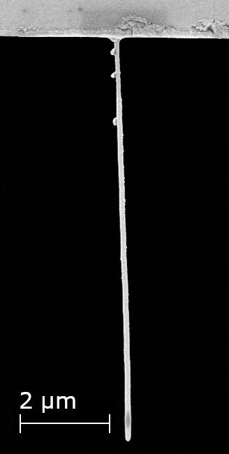
We grow free-standing NWs by FEBID using as a gas precursor at specific positions along the cleaved edge of a Au-coated GaAs chip. Their lengths range from and their base diameters from as inferred from scanning electron microscopy (SEM) images. They consist of nanocrystalline Co, with a composition reaching up to 80% Pablo-Navarro et al. (2017), and residues of C and O. Their proximity to the edge of the chip allows optical access from the side for the detection of their flexural motion. A SEM image of a Co NW standing at the chip edge is shown in Figure 1(a). Surface roughness and geometric irregularities are part of the FEBID fabrication process and are present across the 11 NWs studied in this work.
III Measurement setup
We grow free-standing NWs by FEBID using as a gas precursor at specific positions along the cleaved edge of a Au-coated GaAs chip. Their lengths range from and their base diameters from as inferred from scanning electron microscopy (SEM) images. They consist of nanocrystalline Co, with a composition reaching up to 80% Pablo-Navarro et al. (2017), and residues of C and O. Their proximity to the edge of the chip allows optical access from the side for the detection of their flexural motion. A SEM image of a Co NW standing at the chip edge is shown in Figure 1(a). Surface roughness and geometric irregularities are part of the FEBID fabrication process and are present across the 11 NWs studied in this work.
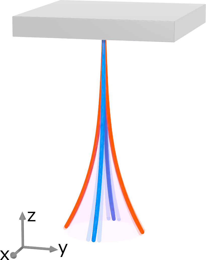
We mount the chip with as-grown Co NWs in a custom-built scanning probe microscope, enclosed in a high-vacuum chamber at a pressure of . The microscope includes a piezoelectric translation stage, with which we position the NW of interest into the focal spot of fiber-coupled optical interferometer for the detection of the NW’s flexural motion Nichol et al. (2008). We use a second piezoelectric translation stage to approach and scan the sample of interest below the NW’s free end, as illustrated in Figure 1(d). This combined apparatus allows us to use individual NWs as scanning probes operating in the pendulum geometry, i.e. with their long axes perpendicular to the sample surface to prevent snapping into contact Rossi et al. (2017, 2019).
| NW | [kHz] | [kHz] | [kHz] | [kg] | |||
|---|---|---|---|---|---|---|---|
| 293 | 1 | 390.726 | 426.018 | 35.292 | 528.0(1.4) | – | 0.69(4) |
| 4 | 514.459 | 556.750 | 42.291 | 551.1(1.5) | 527(66) | 0.260(15) | |
| 4.2 | 4 | 550.803 | 593.745 | 42.942 | 1045(1.0) | 1156(40) | 0.260(15) |
| 4 | 555.860 | 599.044(49) | 43.18 | 2356(39) | – | 0.260(15) |
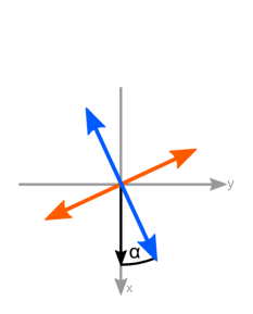
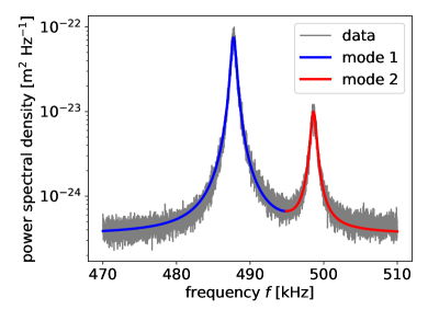
The fiber-coupled optical interferometer operates at and provides a calibrated measurement of the NWs flexural motion projected along the measurement axis (see Appendix A). Figure 1(e) shows a typical power spectral density (PSD) of an individual NW’s thermally excited flexural motion at room temperature, revealing a splitting in resonance frequency of the fundamental mode. This well-known splitting is observed for all examined NWs and is a signature of two nearly degenerate, orthogonal flexural eigenmodes, resulting from cross-sectional asymmetries and/or non-isotropic clamping Cadeddu et al. (2016). The NW’s coupling to the thermal bath results in a Langevin force that drives each mode equally. The difference in the amplitude of the two thermal noise peaks in Figure 1(e) is a consequence of the projection of the NW’s flexural motion onto a single measurement axis, corresponding to the direction of the optical gradient, at an angle with respect to mode 1.
IV Mechanical properties
Measurements of the NWs’ thermo-mechanical noise PSD are performed with the bath held at room temperature (), liquid nitrogen temperature (), and liquid helium temperature (). Heating caused by absorption of the incident laser light can increase the NW’s temperature well above the bath temperature. As a result, care must be taken interpreting PSDs, as discussed in the Supplementary Information. Using the fits to the measured PSDs based on the fluctuation-dissipation theorem, we determine the mechanical properties of the fundamental flexural modes: their resonance frequencies , quality factors (), and effective motional mass (see Appendix A) Rossi et al. (2019). At , the resonance frequencies of the NWs are between and with a mode splitting from . We measure quality factors around 600 and motional masses in the 100s of range. These parameters correspond to flexural modes with effective spring constants of a few . At a bath temperature , the quality factors improve by roughly a factor of 3 to around and the resonance frequencies shift upwards by roughly . From these parameters, shown in Table 1 for two different NWs, we deduce the spring constants, mechanical dissipation, and thermally limited force sensitivities. Notably, at , a typical NW has flexural modes with thermally-limited force sensitivities around . In practice the force sensitivity is limited to about , since even at very low laser power ( on NW 4, signal-to-noise ratio of first mode ) bolometric heating is present and leads to a NW temperature (see Supplementary Information).
V Magnetic properties
We probe the magnetic properties of each NW by measuring its mechanical response to a uniform magnetic field up to applied along its long axis. In particular, we measure the shift in the resonance frequency of each flexural mode, , as a function of , where is the resonance frequency at . Figure 2 shows a typical measurement of the hysteretic response of and carried out on NW 4 with . As in measurements of the other NWs, the data show a smooth V-shaped response for most of the field range, except for discontinuous inversions of the slope (“jumps”) in reverse fields of around . These sharp features, which arise from the switching of the NW magnetization, and the steady stiffening of the mechanical response as increases are characteristic of a strong magnet with a square magnetization hysteresis, whose easy axis is nearly parallel to the applied field Gross et al. (2016). Therefore, the data point to NWs with negligible magnetocrystalline anisotropy and an easy axis coincident with their long axis, as set by the magnetic shape anisotropy resulting from their extreme aspect ratio.
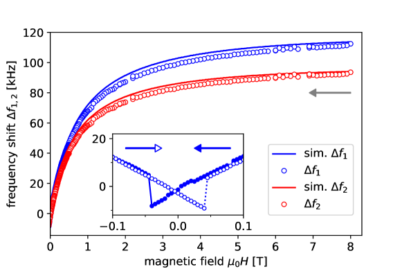
In order to extract specific magnetic properties from our measurements, we compare them to micromagnetic simulations, which model both the NW’s magnetic state and the way in which its interaction with affects the mechanical rigidity of the flexural modes. We use Mumax3 Vansteenkiste et al. (2014); Exl et al. (2014), which employs the Landau-Lifshitz-Gilbert micromagnetic formalism with finite-difference discretization, together with geometrical and material parameters to model each NW. For a given value of in a hysteresis loop, the numerical simulation yields the equilibrium magnetization configuration and the total magnetic energy corresponding to that configuration. Just as in dynamic cantilever magnetometry (DCM) Gross et al. (2016); Mehlin et al. (2018), the frequency shift of each flexural mode is proportional to the curvature of the system’s magnetic energy with respect to rotations corresponding to each mode’s oscillation:
| (1) |
where is an effective length, which takes into account the shape of the flexural mode Stipe et al. (2001). Therefore, by numerically calculating the second derivatives of with respect to at each , we simulate (see Appendix B). Note that, unlike in standard DCM, where the magnetic sample is attached to the end of the cantilever, each NW is magnetic along its full length. Because of the mode shape, different parts of the NW rotate by different angles during a flexural oscillation. This effect must be carefully considered in order to correctly model the system.
The excellent agreement between the measured and simulated in Figure 2 is typical for all measured NWs. For each NW, the mechanical parameters used in the simulation are extracted from measurements of the thermal motion at , while geometrical parameters are estimated from SEM images. We adjust the value of the saturation magnetization in order to bring the curves into agreement, giving us a sensitive measurement of this material property. is found to be , where the uncertainty is dominated by the estimation of the NW geometry from SEM. This value compares well with the expected Co composition of the FEBID NWs and literature values for the saturation magnetization of Co, as well as with electron holography measurements of similar NWs Pablo-Navarro et al. (2017). In addition, the simulations show that the magnetization of the NWs is axially aligned in remanence for up to about of reverse field. These results are consistent with nanoSQUID measurements of similar Co NWs carried out at 15 K by Martínez-Pérez et al Martínez-Pérez et al. (2018). This axially aligned remanent magnetization can be represented by a magnetic charge distribution in the form of an elongated dipole, leaving a monopole-like distribution localized at the free end of the NW to interact with an underlying sample, as shown in Figure 3d.
VI Measurement of magnetic field profile
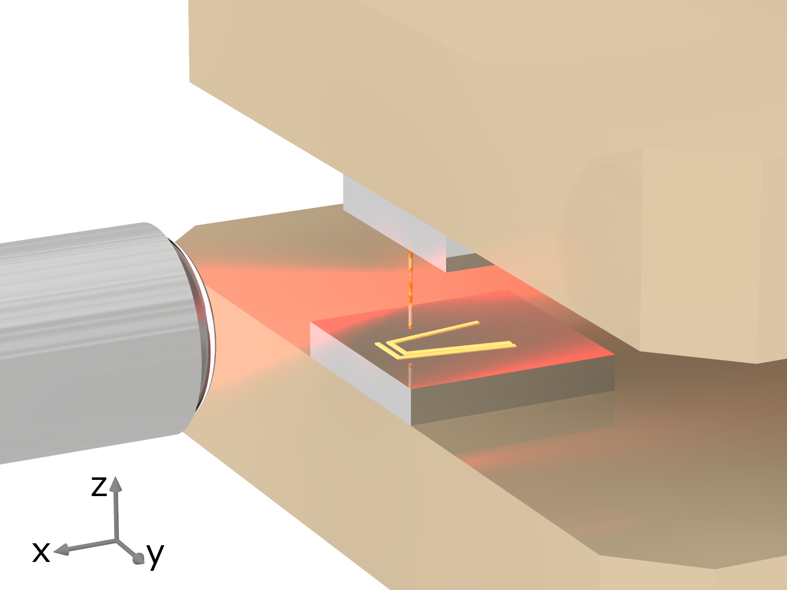
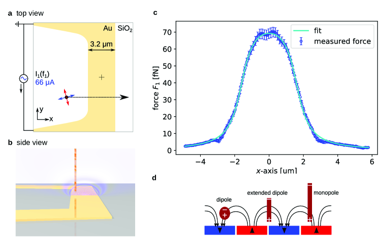
In order to determine the behavior of the FEBID NWs as scanning probes, we approach and scan a nearly planar sample with respect to NW 4 at . The sample consists of a -long, -wide, and -thick Au wire patterned between two contact pads on a Si substrate (Figure 3a and b). By passing a current through the wire, we produce a well-known magnetic field profile given by the Biot-Savart relation, with which we drive NW oscillations and calibrate its response, as done in standard MFM Lohau et al. (1999); Schendel et al. (2000); Kebe and Carl (2004). By applying an excitation current containing two sine waves, each at the frequency of one of the NW modes and , we drive the NW as we scan it across the Au wire at a fixed tip-sample spacing. Both the resonance frequencies and oscillation amplitudes are tracked using two phase-locked loops. The corresponding values of the force driving each mode on resonance are calculated using (see Supplementary Information). Figure 3c shows the response of mode 1 for a drive current amplitude of as the NW is scanned above the Au wire at a fixed distance in the absense of static magnetic field (). Since the first mode is nearly aligned with the -direction () and thus along the direction of , the orthogonal second mode has almost no response to the driving tone at and is not shown.
From our torque magnetometry measurements, we know that the magnetic NWs have an axially aligned remanent magnetization. Because the decay length of the magnetic field from our sample is much shorter than the NW length, the sample fields only interact with the monopole-like magnetic charge distribution at the free end of the NW Hug et al. (1998). This charge distribution then determines the NW’s response to magnetic field profiles produced by a sample. For a monopole-like NW tip, we can relate the driving magnetic field and the force it produces on the NW by
| (2) |
where is an effective magnetic monopole moment describing the tip magnetization and is the unit vector in the direction of displacement of mode . In this point-probe approximation, we consider the interaction of dipole and higher multipoles of the magnetic charge with the driving field to be negligible. As shown by the agreement between the field calculated from the Biot-Savart law and the measured response of NW 4 in Figure 3c, this approximation is valid for our NWs. Control experiments, using the applied magnetic field to initialize the NW magnetization along the opposite direction also show that spurious electrostatic driving of the NW modes is negligible. Combining measurements at different and different driving currents, we find that NW 4 has an effective magnetic charge of . Given our thermally limited force sensitivity of at , this value of gives our sensors a sensitivity to magnetic field of around . This sensitivity is similar to those of some of the most sensitive scanning probes available, including scanning NV magnetometers and scanning SQUIDs.
Furthermore, the magnetic charge model allows us to estimate the stray field and field gradients produced by the NW tip, so that we can assess its potential for perturbing the magnetic state of the sample below. At a distance of from the NW tip, the stray magnetic field and magnetic field gradients are and . The stray field is of similar size to that produced by a conventional MFM tip Zhu (2005). For future NW devices to be less invasive, i.e. having less magnetic charge at their tips, sharper tips than those produced here, which are more than 100 nm in diameter, will be required Berganza et al. (2018). The large magnetic field gradients, however, combined with the NWs’ excellent force sensitivity may make the NWs well-suited as transducers in sensitive magnetic resonance force microscopy Poggio and Degen (2010).
VII Magnetic field imaging
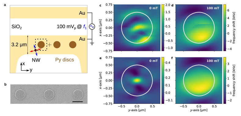
In Figure 4, we demonstrate the ability to image sub-micrometer features using a FEBID NW as MFM sensor on a permalloy disk (Ni0.81Fe0.19) at . Three disks, in diameter and -thick, are patterned on top of the Au wire, of which one is imaged. During the scan, the first flexural mode of the NW is electrically driven on resonance using an AC voltage applied between the Au wire and a third lead (Figure 4a). Frequency shift and dissipation are recorded using a phase-locked loop. Figures 4c and d show a image of frequency shift , as the disk is scanned below NW 4 for at and for at , respectively. At (Figure 4c), the magnetization of the disk is arranged in a remanent vortex configuration Badea et al. (2015), as verified by a micromagnetic simulation carried out with Mumax3. Figure 4e shows the magnetic image contrast expected from the simulation using the monopole model (2), in which the frequency shift of the NW mode is proportional to the stray field derivative along the mode direction. While the contrast measured at the edges of the disk is due to topographic features, the contrast in the center is consistent with what is expected from the stray field of a vortex core. The image taken at , Figure 4d, shows an almost homogeneous magnetic imaging contrast across the disk. The corresponding simulation in Figure 4f agrees well with the measurement and reveals that while the vortex core is still present in the center of the disk, its stray field is overshadowed by the field originating from the outer parts of the disk, where the magnetization tilts out of plane. The region of high frequency shift in the bottom right quadrant of Figure 4d is explained in the simulation by assuming a small tilt () of the disk plane with respect to the external field, resulting in the vortex core being slighltly offset from the center of the disk. Although a detailed interpretation of the NW MFM images and a quantitative comparison of the measured and calculated frequency shifts is beyond the scope of this work, they showcase the high sensitivity and potential spatial resolution of the FEBID NWs transducers.
VIII Conclusion
In the past, FEBID-grown NWs have been patterned directly on tips of atomic force microscopy (AFM) cantilevers in an effort to improve spatial resolution Utke et al. (2002); Stiller et al. (2017); Berganza et al. (2018). Our results make clear that such nanocrystalline metallic NWs can have surprisingly high mechanical quality, making FEBID a promising and versatile method for producing nanometer-scale force transducers. In principle, a FEBID NW patterned on the tip of a standard AFM or MFM cantilever could be used to add sensitive 2D lateral force and dissipation detection capabilities. Such a system would be capable of vectorial force sensing in 3D, i.e. mapping both the size and the direction in 3D of tip-sample forces.
In addition to demonstrating the high-force sensitivity of FEBID-grown NWs, we also show their excellent magnetic properties. The Co NWs measured here maintain a saturation magnetization, which is 80% of the value of pure Co. They also have an axially aligned remanent magnetization with a switching field around . These magnetic properties, combined with the aforementioned mechanical properties, make these NWs among the most sensitive sensors of local magnetic field. The ability to fine tune the NW geometry, especially making them thinner and sharper, may allow for even better field sensitivities and spatial resolutions in the future. NW MFM with such transducers may prove ideal for investigating subtle magnetization textures and current distributions on the nanometer-scale, which – so far – have been inaccessible by other methods.
Appendix A Interferometric Measurement of Flexural Motion
We use a custom-built interferometer to detect the thermal or driven motion of the NW of interest. At its heart is a four arm fiber coupler with a 95:5 coupling ratio. A Toptica wavelength laser is connected to the input port and can be attenuated to the desired power. At the experiment arm of the fiber coupler ( transmission), an objective with a high numerical aperture focuses the laser light with a beam waist of around onto the NW. The interferometric displacement signal arises from the weak cavity between the NW and the end facet of the optical fiber. At the signal port of the fiber coupler the signal is converted to a voltage by a Femto OE-300 photoreceiver and subsequently split into its DC and AC parts. Knowing the wavelength of the laser, the conversion factor between displacement and voltage can be determined accurately and is usually in the range of a few . A more detailed description of the optical setup can be found in the supplementary information of Ref. Rossi et al. (2019).
The thermal displacement noise PSD, which is the projection of the motion of the two first order flexural modes onto the direction of the local optical gradient, can be described by the fluctuation-dissipation theorem following the derivations in Ref. Braakman and Poggio (2019) as,
| (3) |
where is the mode shape, the Boltzmann constant, and the effective temperature and mass of the NW resonator, and the resonance frequencies and quality factors of the two first order flexural modes, the measurement angle between the direction of the first mode and the optical gradient, and the background noise. Depending on the position of the NW inside the beam waist, the optical gradient direction can be chosen at will. Ideally, however, it is aligned with the optical axis in order to achieve the best signal-to-noise ratio. The -direction is aligned with the NW axis and its origin is located at the base of the NW. From the fit parameters, the spring constants and the thermally limited force sensitivity can be calculated.
Appendix B Micromagnetic Simulations
The principles of simulating the torque magnetometry signal with micromagnetic solvers are described in Refs. Gross et al. (2016); Mehlin et al. (2015); Rossi et al. (2019). In these works, it is only the tip of the mechanical resonator which is magnetic, therefore the system can be modelled as a magnetic object oscillating in a homogeneous external magnetic field. The mode shape of the mechanical resonator enters into the calculation only in the form of the effective length, simplifying the mechanics to that of a harmonic oscillator. For the Co NWs, which are both the mechanical resonator and the magnetic object, the mode shape has to be taken into account. Each longitudinal segment of the NW rotates by a different angle during a flexural oscillation, experiencing a different tilt of the external magnetic field. We account for this effect by applying a spatially dependent external field in the simulation, rather than altering the geometry, which is impractical. For positive (negative) deflections in experiment, the tilt direction of the field in the simulations increases (decreases) with the position along the NW. The magnitude of the tilt angle follows the Euler-Bernoulli equation, reflecting the mode shape. We choose a maximum oscillation amplitude (at the tip) large enough to account for the finite precision of the simulation. The torque signal can then be calculated using the magnetic energy of the system for small positive, negative, and no deflection given by the simulation combined with a finite difference approximation for the second derivative in equation (1) Mehlin et al. (2018).
The final geometry used in the simulation of Figure 2 is a long, elliptic cylinder, whose diameters are modulated along the direction, as determined from the SEM images. The average diameters along the two mode directions are and . Space is discretized to . Material parameter values are the saturation magnetization and the exchange stiffness . The latter has been chosen to match the switching field of the NW, and is significantly larger than other values reported for Co Shirane et al. (1968); Vernon et al. (1984); Krishnan (1985); Liu et al. (1996). This discrepancy arises because the switching field also depends sensitively on geometrical and material imperfections, which we do not attempt to model. Nevertheless, control simulations confirm that the overall magnetization reversal process and the remanent states are unaffected by such differences in .
In an effort to determine the effect of nanocrystallinity in the NW, we have run simulations with NW divided into grains of around size, giving each grain a uniaxial anisotropy with and a random orientation of the anisotropy axis. We find that this refinement does not significantly change the simulation results with respect to standard simulations assuming homogeneous material without crystalline anisotropy.
Acknowledgements.
We thank Sascha Martin and his team in the machine shop of the Physics Department at the University of Basel for help building the measurement system. We acknowledge the support of the Kanton Aargau, the ERC through Starting Grant NWScan (Grant 334767), the SNF under Grant 200020-178863, the Swiss Nanoscience Institute, and the NCCR Quantum Science and Technology (QSIT) as well as from the Spanish Ministry of Economy and Competitiveness (MINECO) through the projects MAT2017-82970-C1 and MAT2017-82970-C2 and from the Aragon Regional Government (Construyendo Europa desde Aragón) through project E13_17R, with European Social Fund funding. J. P.-N. grant is funded by the Ayuda para Contratos Predoctorales para la Formación de Doctores, Convocatoria Res. 05/06/15 (BOE 12/06/15) of the Secretaría de Estado de Investigación, Desarrollo e Innovación in the Subprograma Estatal de Formación of the Spanish Ministry of Economy and Competitiveness with the participation of the European Social Fund.References
- Yu et al. (2010) X. Z. Yu, Y. Onose, N. Kanazawa, J. H. Park, J. H. Han, Y. Matsui, N. Nagaosa, and Y. Tokura, Real-space observation of a two-dimensional skyrmion crystal, Nature 465, 901 (2010).
- Nowack et al. (2013) K. C. Nowack, E. M. Spanton, M. Baenninger, M. König, J. R. Kirtley, B. Kalisky, C. Ames, P. Leubner, C. Brüne, H. Buhmann, L. W. Molenkamp, D. Goldhaber-Gordon, and K. A. Moler, Imaging currents in HgTe quantum wells in the quantum spin Hall regime, Nature Materials 12, 787 (2013).
- Thiel et al. (2019) L. Thiel, Z. Wang, M. A. Tschudin, D. Rohner, I. Gutiérrez-Lezama, N. Ubrig, M. Gibertini, E. Giannini, A. F. Morpurgo, and P. Maletinsky, Probing magnetism in 2d materials at the nanoscale with single-spin microscopy, Science 364, 973 (2019).
- Jelić et al. (2017) Ž. L. Jelić, A. Gurevich, A. V. Silhanek, E. O. Lachman, E. Zeldov, G. P. Mikitik, L. Embon, M. E. Huber, M. V. Milošević, Y. Anahory, and Y. Myasoedov, Imaging of super-fast dynamics and flow instabilities of superconducting vortices, Nature Communications 8, 85 (2017).
- Uri et al. (2019) A. Uri, Y. Kim, K. Bagani, C. K. Lewandowski, S. Grover, N. Auerbach, E. O. Lachman, Y. Myasoedov, T. Taniguchi, K. Watanabe, J. Smet, and E. Zeldov, Nanoscale imaging of equilibrium quantum Hall edge currents and of the magnetic monopole response in graphene, arXiv:1908.02466 (2019).
- Hicks et al. (2007) C. W. Hicks, L. Luan, K. A. Moler, E. Zeldov, and H. Shtrikman, Noise characteristics of 100nm scale GaAs/AlxGa1-xAs scanning Hall probes, Applied Physics Letters 90, 133512 (2007).
- Maletinsky et al. (2012) P. Maletinsky, S. Hong, M. S. Grinolds, B. Hausmann, M. D. Lukin, R. L. Walsworth, M. Loncar, and A. Yacoby, A robust scanning diamond sensor for nanoscale imaging with single nitrogen-vacancy centres, Nature Nanotechnology 7, 320 (2012).
- Vasyukov et al. (2013) D. Vasyukov, Y. Anahory, L. Embon, D. Halbertal, J. Cuppens, L. Neeman, A. Finkler, Y. Segev, Y. Myasoedov, M. L. Rappaport, M. E. Huber, and E. Zeldov, A scanning superconducting quantum interference device with single electron spin sensitivity, Nature Nanotechnology 8, 639 (2013).
- Rossi et al. (2019) N. Rossi, B. Gross, F. Dirnberger, D. Bougeard, and M. Poggio, Magnetic Force Sensing Using a Self-Assembled Nanowire, Nano Letters 19, 930 (2019).
- Braakman and Poggio (2019) F. R. Braakman and M. Poggio, Force sensing with nanowire cantilevers, Nanotechnology 30, 332001 (2019).
- Randolph et al. (2006) S. J. Randolph, J. D. Fowlkes, and P. D. Rack, Focused, Nanoscale Electron-Beam-Induced Deposition and Etching, Critical Reviews in Solid State and Materials Sciences 31, 55 (2006).
- van Dorp and Hagen (2008) W. F. van Dorp and C. W. Hagen, A critical literature review of focused electron beam induced deposition, Journal of Applied Physics 104, 081301 (2008).
- Utke et al. (2008) I. Utke, P. Hoffmann, and J. Melngailis, Gas-assisted focused electron beam and ion beam processing and fabrication, Journal of Vacuum Science & Technology B: Microelectronics and Nanometer Structures Processing, Measurement, and Phenomena 26, 1197 (2008).
- Huth et al. (2012) M. Huth, F. Porrati, C. Schwalb, M. Winhold, R. Sachser, M. Dukic, J. Adams, and G. Fantner, Focused electron beam induced deposition: A perspective, Beilstein Journal of Nanotechnology 3, 597 (2012).
- Utke et al. (2012) I. Utke, S. Moshkalev, and P. Russell, eds., Nanofabrication Using Focused Ion and Electron Beams: Principles and Applications (Oxford University Press, Oxford, New York, 2012).
- Gannon et al. (2004) T. J. Gannon, G. Gu, J. D. Casey, C. Huynh, N. Bassom, and N. Antoniou, Focused ion beam induced deposition of low-resistivity copper material, Journal of Vacuum Science & Technology B: Microelectronics and Nanometer Structures Processing, Measurement, and Phenomena 22, 3000 (2004).
- Wu et al. (2014) H. Wu, L. A. Stern, D. Xia, D. Ferranti, B. Thompson, K. L. Klein, C. M. Gonzalez, and P. D. Rack, Focused helium ion beam deposited low resistivity cobalt metal lines with 10 nm resolution: implications for advanced circuit editing, Journal of Materials Science: Materials in Electronics 25, 587 (2014).
- Teresa et al. (2016) J. M. D. Teresa, A. Fernández-Pacheco, R. Córdoba, L. Serrano-Ramón, S. Sangiao, and M. R. Ibarra, Review of magnetic nanostructures grown by focused electron beam induced deposition (FEBID), Journal of Physics D: Applied Physics 49, 243003 (2016).
- Sadki et al. (2004) E. S. Sadki, S. Ooi, and K. Hirata, Focused-ion-beam-induced deposition of superconducting nanowires, Applied Physics Letters 85, 6206 (2004).
- Esposito et al. (2015) M. Esposito, V. Tasco, M. Cuscunà, F. Todisco, A. Benedetti, I. Tarantini, M. D. Giorgi, D. Sanvitto, and A. Passaseo, Nanoscale 3d Chiral Plasmonic Helices with Circular Dichroism at Visible Frequencies, ACS Photonics 2, 105 (2015).
- Bret et al. (2014) T. Bret, T. Hofmann, and K. Edinger, Industrial perspective on focused electron beam-induced processes, Applied Physics A 117, 1607 (2014).
- Giannuzzi and Stevie (1999) L. A. Giannuzzi and F. A. Stevie, A review of focused ion beam milling techniques for TEM specimen preparation, Micron 30, 197 (1999).
- Nanda et al. (2015) G. Nanda, E. van Veldhoven, D. Maas, H. Sadeghian, and P. F. A. Alkemade, Helium ion beam induced growth of hammerhead AFM probes, Journal of Vacuum Science & Technology B 33, 06F503 (2015).
- Schwalb et al. (2010) C. H. Schwalb, C. Grimm, M. Baranowski, R. Sachser, F. Porrati, H. Reith, P. Das, J. Müller, F. Völklein, A. Kaya, and M. Huth, A Tunable Strain Sensor Using Nanogranular Metals, Sensors 10, 9847 (2010).
- Córdoba et al. (2018) R. Córdoba, A. Ibarra, D. Mailly, and J. M. De Teresa, Vertical Growth of Superconducting Crystalline Hollow Nanowires by He+ Focused Ion Beam Induced Deposition, Nano Letters 18, 1379 (2018).
- Pablo-Navarro et al. (2017) J. Pablo-Navarro, D. Sanz-Hernández, C. Magén, A. Fernández-Pacheco, and J. M. d. Teresa, Tuning shape, composition and magnetization of 3d cobalt nanowires grown by focused electron beam induced deposition (FEBID), Journal of Physics D: Applied Physics 50, 18LT01 (2017).
- Nichol et al. (2008) J. M. Nichol, E. R. Hemesath, L. J. Lauhon, and R. Budakian, Displacement detection of silicon nanowires by polarization-enhanced fiber-optic interferometry, Applied Physics Letters 93, 193110 (2008).
- Rossi et al. (2017) N. Rossi, F. R. Braakman, D. Cadeddu, D. Vasyukov, G. Tütüncüoglu, A. Fontcuberta i Morral, and M. Poggio, Vectorial scanning force microscopy using a nanowire sensor, Nature Nanotechnology 12, 150 (2017).
- Cadeddu et al. (2016) D. Cadeddu, F. R. Braakman, G. Tütüncüoglu, F. Matteini, D. Rüffer, A. Fontcuberta i Morral, and M. Poggio, Time-Resolved Nonlinear Coupling between Orthogonal Flexural Modes of a Pristine GaAs Nanowire, Nano Letters 16, 926 (2016).
- Gross et al. (2016) B. Gross, D. P. Weber, D. Rüffer, A. Buchter, F. Heimbach, A. Fontcuberta i Morral, D. Grundler, and M. Poggio, Dynamic cantilever magnetometry of individual CoFeB nanotubes, Physical Review B 93, 064409 (2016).
- Vansteenkiste et al. (2014) A. Vansteenkiste, J. Leliaert, M. Dvornik, M. Helsen, F. Garcia-Sanchez, and B. Van Waeyenberge, The design and verification of MuMax3, AIP Advances 4, 107133 (2014).
- Exl et al. (2014) L. Exl, S. Bance, F. Reichel, T. Schrefl, H. Peter Stimming, and N. J. Mauser, LaBonte’s method revisited: An effective steepest descent method for micromagnetic energy minimization, Journal of Applied Physics 115, 17D118 (2014).
- Mehlin et al. (2018) A. Mehlin, B. Gross, M. Wyss, T. Schefer, G. Tütüncüoglu, F. Heimbach, A. Fontcuberta i Morral, D. Grundler, and M. Poggio, Observation of end-vortex nucleation in individual ferromagnetic nanotubes, Physical Review B 97, 134422 (2018).
- Stipe et al. (2001) B. C. Stipe, H. J. Mamin, T. D. Stowe, T. W. Kenny, and D. Rugar, Magnetic Dissipation and Fluctuations in Individual Nanomagnets Measured by Ultrasensitive Cantilever Magnetometry, Physical Review Letters 86, 2874 (2001).
- Martínez-Pérez et al. (2018) M. J. Martínez-Pérez, J. Pablo-Navarro, B. Müller, R. Kleiner, C. Magén, D. Koelle, J. M. de Teresa, and J. Sesé, NanoSQUID Magnetometry on Individual As-grown and Annealed Co Nanowires at Variable Temperature, Nano Lett. 18, 7674 (2018).
- Hug et al. (1998) H. J. Hug, B. Stiefel, P. J. A. v. Schendel, A. Moser, R. Hofer, S. Martin, H.-J. Güntherodt, S. Porthun, L. Abelmann, J. C. Lodder, G. Bochi, and R. C. O’Handley, Quantitative magnetic force microscopy on perpendicularly magnetized samples, Journal of Applied Physics 83, 5609 (1998).
- Lohau et al. (1999) J. Lohau, S. Kirsch, A. Carl, G. Dumpich, and E. F. Wassermann, Quantitative determination of effective dipole and monopole moments of magnetic force microscopy tips, Journal of Applied Physics 86, 3410 (1999).
- Schendel et al. (2000) P. J. A. v. Schendel, H. J. Hug, B. Stiefel, S. Martin, and H.-J. Güntherodt, A method for the calibration of magnetic force microscopy tips, Journal of Applied Physics 88, 435 (2000).
- Kebe and Carl (2004) T. Kebe and A. Carl, Calibration of magnetic force microscopy tips by using nanoscale current-carrying parallel wires, Journal of Applied Physics 95, 775 (2004).
- Zhu (2005) Y. Zhu, ed., Modern Techniques for Characterizing Magnetic Materials (Springer US, 2005).
- Berganza et al. (2018) E. Berganza, M. Jaafar, M. Goiriena-Goikoetxea, J. Pablo-Navarro, A. Garcia-Arribas, K. Gusliyenko, C. Magen, J. M. de Teresa, O. Chubykalo-Fesenko, and A. Asenjo, Observation of hedgehog skyrmions in sub-100 nm soft magnetic nanodots, arXiv:1803.08768 (2018).
- Poggio and Degen (2010) M. Poggio and C. L. Degen, Force-detected nuclear magnetic resonance: recent advances and future challenges, Nanotechnology 21, 342001 (2010).
- Badea et al. (2015) R. Badea, J. A. Frey, and J. Berezovsky, Magneto-optical imaging of vortex domain deformation in pinning sites, Journal of Magnetism and Magnetic Materials 381, 463 (2015).
- Utke et al. (2002) I. Utke, P. Hoffmann, R. Berger, and L. Scandella, High-resolution magnetic Co supertips grown by a focused electron beam, Applied Physics Letters 80, 4792 (2002).
- Stiller et al. (2017) M. Stiller, J. Barzola-Quiquia, P. D. Esquinazi, S. Sangiao, J. M. D. Teresa, J. Meijer, and B. Abel, Functionalized Akiyama tips for magnetic force microscopy measurements, Measurement Science and Technology 28, 125401 (2017).
- Mehlin et al. (2015) A. Mehlin, F. Xue, D. Liang, H. F. Du, M. J. Stolt, S. Jin, M. L. Tian, and M. Poggio, Stabilized Skyrmion Phase Detected in MnSi Nanowires by Dynamic Cantilever Magnetometry, Nano Letters 15, 4839 (2015).
- Shirane et al. (1968) G. Shirane, V. J. Minkiewicz, and R. Nathans, Spin Waves in 3d Metals, Journal of Applied Physics 39, 383 (1968).
- Vernon et al. (1984) S. P. Vernon, S. Lindsay, and M. B. Stearns, Brillouin scattering from thermal magnons in a thin Co film, Physical Review B 29, 4439 (1984).
- Krishnan (1985) R. Krishnan, FMR studies in compositionally modulated Co-Nb and Co films, Journal of Magnetism and Magnetic Materials 50, 189 (1985).
- Liu et al. (1996) X. Liu, M. M. Steiner, R. Sooryakumar, G. A. Prinz, R. F. C. Farrow, and G. Harp, Exchange stiffness, magnetization, and spin waves in cubic and hexagonal phases of cobalt, Physical Review B 53, 12166 (1996).