Modulation of heat transport in two-dimensional group-III chalcogenides
Abstract
We systematically investigated the modulation of heat transport of experimentally accessible two-dimensional (2D) group-III chalcogenides by first-principles calculations. It was found that intrinsic thermal conductivity () of chalcogenides MX (M = Ga, In; X = S, Se) were desirable for efficient heat dissipation. Meanwhile, we showed that the long-range anharmonic interactions played an important role in heat transport of the chalcogenides. The difference of among the 2D group-III chalcogenides can be well described by the Slack model and can be mainly attributed to phonon group velocity. Based on that, we proposed three methods including strain engineering, size effect and making Janus structures to effectively modulate the of 2D group-III chalcogenides, with different underlying mechanisms. We found that tensile strain and rough boundary scattering could continuously decrease the while compressive strain could increase the of 2D group-III chalcogenides. On the other side, the change of by producing Janus structures is permanent and dependent on the structural details. These results provide guilds to modulate heat transport properties of 2D group-III chalcogenides for devices application.
,
-
May 2019
Keywords: group-III chalcogenides, thermal transport, strain, Janus structure
1 Introduction
Two-dimensional (2D) materials with high carrier mobility () have great potential applications in future electronic, optoelectronic and thermoelectric devices [1, 2, 3]. These applications are inevitably related to heat management and heat rectification in devices. A high thermal conductivity () is requested for fast heat dissipation of nanoscale electronic devices [4]. Contrary to that, nanoscale thermoelectric devices with high conversion efficiency require a high and a low at the same time [5]. Thus, the understanding and modulation of thermal transport properties of 2D materials with high are of technological importance for relevant device performance.
The well-known graphene [6] and 2D MoS2 [7] suffers from the lack of a natural band gap and the low , respectively. Phosphorene has a high , but its will degrade at atmosphere condition [8]. Group-III chalcogenides including GaS, GaSe and InSe are hexagonal layered semiconductor and consists of quadruple sublayers (see Fig. 1(b)) which are held together by van der Waals (vdW) interactions [9]. Group-III chalcogenides have attracted great interest recently due to their superior properties, such as direct band gap, small effective mass, rare p-type electronic behaviors, high charge density, and so on [10]. Recently, 2D InSe were demonstrated to have a high electron ( cm2/(Vs)) [11, 12] which is comparable with its bulk counterpart [13]. On the other side, the bendable photodetectors based on 2D GaS [14], GaSe [15] and InSe [16] have a ultrahigh photoresponsivity, detectivity and a broadband spectral response on flexible and transparent mica substrates, regardless of repeated bending [9]. Moreover, nano-devices base on 2D InSe and GaSe have demonstrated to have good ambient stability [17, 18].
These advantages have intrigued many works on the electrical and optoelectronic properties of 2D group-III chalcogenides [19, 20, 21, 22, 23, 24]. It also call for a systematical investigation to phonon transport properties and its modulation of 2D group-III chalcogenides, which is still limited [25, 26]. Besides, though 2D InS with InSe-like structure has been synthesized, its thermal properties have not been investigated [27]. In this work, we studied the heat transport of monolayer group-III chalcogenides by first-principles calculations, coupled with phonon Boltzmann transport equation (BTE). We first calculated the intrinsic thermal conductivity of chalcogenides MX (M = Ga, In; X = S, Se) and found their can be well described by the Slack model. Meanwhile, we showed the important role of long-range anharmonic interaction in the heat transport of group-III chalcogenides. Based on that, taking monolayer InSe as an example, we displayed three effective approaches to modulate of 2D group-III chalcogenides including strain engineering, nanostructuring, and producing Janus structure.
2 Methodology
Based on the phonon BTE, lattice thermal conductivity is calculates by [28]
| (1) |
where and is the number of point and volume of the unit cell, respectively. and are Cartesian indices. , and is the mode specific capacity, phonon group velocity and lifetime of the phonon mode with wavevector and branch index , respectively. The scattering mechanism to estimate phonon lifetime includes the anharmonic scattering (), isotopic impurities scattering () and boundary roughness scattering with be the sample size. The computational details are given in the supplemental material.
3 Results and discussion
3.1 The thermal conductivity of monolayer group-III chalcogenides
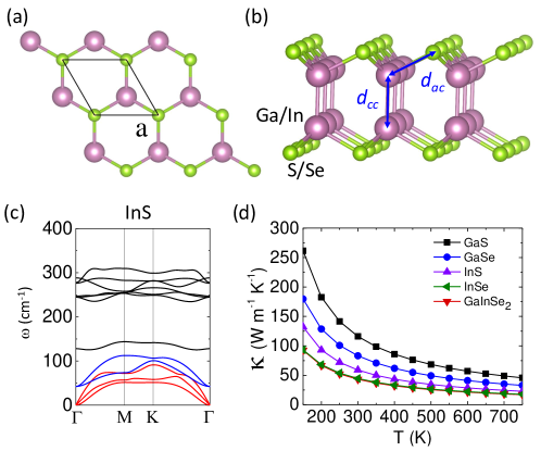
Figure 1(a) and 1 (b) display the crystal structure of monolayer group-III chalcogenides, which has the crystal symmetry. The optimized lattice constants, bond lengths (labeled in Fig. 1(b)) and thickness of monolayer are listed in Table S1 in the supplementary material. 2D group-III chalcogenides are semiconductors [10] and the heat is mainly carried by lattice vibrations. The phonon dispersion of monolayer InS and other materials are displayed in Fig. 1(c) and Fig. S1 to display its lattice stability. The acoustic branches (see red line in Fig. 1(c)) consist of the in-plane longitudinal (LA) branch, transverse (TA) branch and out-of-plane flexural branch (ZA) branch.
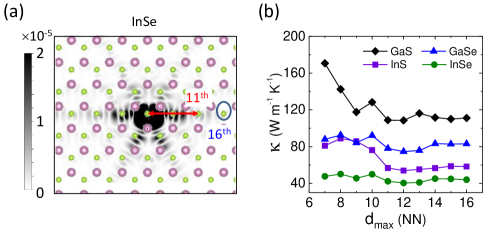
We found that long-range anharmonic interatomic force constants ( IFCs) is a common feature in monolayer group-III chalcogenides. It can be directly reflected by the response of charge density to perturbations of the atomic displacements. Taking InSe as an example, we induced a small distortion ( Å) to the central Se atoms along the zigzag or armchair direction. As a result, the disturbance of the absolute charge density is particularly extended along the zigzag direction, as shown in Fig. 2(a). A clear at the zone with distance from origin Se atoms less than of 8.19 Å which corresponds to nearest neighbors (NN). Furthermore, the non-negligible can take place as long as 10 Å ( NN), as shown in Fig. 2(a). Similar to our previous work [29], for the IFCs of four group-III chalcogenides, we extracted its maximum component of and the maximum interatomic distance () between three atoms (, , ) [30]. The distribution of with respect to is shown in Fig. S2. We identified that the triplets are particularly large at the and NN for all the group-III chalcogenides. Meanwhile, the populations of the IFCs as the function of are shown in the inset of Fig. S2. We found that though the triplets at NN are small, it has a particularly large population. The distribution of IFCs is consistent with the aforementioned distribution of . The convergence test of the of monolayer group-III chalcogenides shows that happens a clear change (see Fig. 2(b)) when we include the IFCs within the of neighbors and neighbors in the calculation of anharmonic relaxation time . That can be understood from the aforementioned large size and large population of IFCs at these distances. The can reach convergence at of NN (see Fig. 2(b)), consistent with previous charge density to perturbations of the atomic displacements.
The intrinsic of monolayer group-III chalcogenides without boundary scattering are calculated at different temperatures (T), as shown in Fig. 1(d). It corresponds according to the Matthiessen rule. The overall of is in the decreasing order of GaS, GaSe, InS and InSe. At T = 300 K, the of monolayer GaS, GaSe, InS and InSe is estimated to be 111.0, 83.10, 58.9 and 44.9 W/(mK), which is compatible with the previous work [26]. The of monolayer group-III chalcogenides are comparable with that of conventional bulk Ge (65 W/(mK) [31]) and GaAs (45 W/(mK) [31]), and larger than of phosphorene which is about 20 W/(mK) along zigzag direaction [32, 33]. Therefore, the intrinsic of 2D group-III chalcogenides are desirable for efficient heat dissipation.
| GaS | 50.90 | 81.32 | 136.5 | 0.63 |
| GaSe | 74.34 | 69.46 | 105.9 | 0.58 |
| InS | 73.45 | 56.50 | 90.1 | 0.45 |
| InSe | 96.89 | 49.21 | 76.3 | 0.51 |
To understand the physical factors that affect heat transport of chalcogenides, we adopted the Slack model which gives as [34],
| (2) |
where B is a numerical coefficient; is the average atomic mass; is the number of atoms in the unit cell; gives the volume per atom; and is the acoustic Debye temperature and Grüneisen parameter, respectively. The simulation details are given in the supplementary material. The results are shown in Table 1.
A large acoustic reflects a large bandwidth of acoustic branches and a large phonon group velocity. Based on a diatomic chain model which contains two types of atoms per unit cell, the mass of heavy atom and bonding stiffness have a negative and positive effect on the acoustic group velocity. In 2D group-III chalcogenides, the bonding stiffness can be described by 2D elastic module [35]. From GaS to InSe, the mass of the heavy atom and is in the increasing and decreasing order, respectively (see Table 1). Thus, the overall order of of acoustic phonons from high to low is in the sequence of GaS, GaSe, InS and InSe (see Fig. S4(a)), which agrees with the order of (see Table 1). The Grüneisen parameter , however, is in the increasing sequence of InS, InSe, GaSe and GaS, which is almost opposite to order of .
Substituting these results into Eq. 2, the ratio of room-temperature of monolayer GaS, GaSe, InS and InSe is , consistent with that obtained by phonon BTE which is . The deviation arises from the neglecting the contribution of low-frequency optical branches (labeled by blue in Fig. 1(c)) to in slack model whereas those phonon modes make a non-negligible contribution to of chalcogenides (see Fig. S3). Thus, the in Eq. 2 ultimately overtake the and other factors, dominating the overall behaviour of of 2D group-III chalcogenides.
From the other side, we also performed a detailed analysis of mode contribution to total . The is given by , where , and are specific heat per unit volume, group velocities and lifetimes of phonon mode with momentum and branch index , respectively. is determined by both the Grüneisen parameter and phase space for phonon anharmonic scattering [36]. In the low-frequency zone, however, there is a competition between and . This makes the of low-frequency phonons in different chalcogenides have almost the same order of magnitude (see Fig. S4(b-d)). Meanwhile, approaches the classic value at a temperature higher than . Thus, the difference of among chalcogenides is mainly determined by phonon group velocity, which is consistent with previous analysis by Slack model.

3.2 The methods to modulate the lattice conductivity
Thermal engineering of 2D material is significant to improve the transport properties and expand its application perspective. Considering group-III chalcogenides share common features in structural symmetry, IFCs and thermal transport model, in the following, we only considered feasible methods to modulate the of 2D InSe, the conclusion will be the same with other group-III chalcogenides.
3.2.1 Strain engineering
Experimentally, strain engineering can be utilized to manipulate the heat transport of 2D materials [37]. we defined the strain as , where and is the lattice constants of monolayer InSe with and without strain, respectively. When applying tensile strain, both and are enlarged and the bonding are weakened. The phonon dispersion curves downshift except that the frequency of ZA phonons is slightly enhanced (see Fig. 3(a)). This leads to overall smaller phonon group velocities and smaller Debye temperature . We calculated the parameters of Eq. 2 at both tensile strain and compressive strain. Grüneisen parameter at different strains can be estimated by alternative approximated finite displacement difference method rather than IFCs calculations [38]. For strain-free monolayer InSe, it gives =0.53 which agrees with =0.50 obtained by calculation of and IFCs. The frequency of phonon and force constants are known to have a negative and positive correlation with [39], leading to complex behavior of with respect to strain . In monolayer InSe, we found that increases as tensile increase (see Fig. 3(b)). Thus, the decrease of and increase of lead to the decrease of of monolayer InSe under tensile strain according to Slack mode [34]. That is similar to many bulk materials [40] and other 2D materials such as MoS2 [41]. On the other side, the compressive strain will decrease the of 2D InSe. We have also calculated the of monolayer InSe under tensile strain of =2.0% and =4.0% through more exact phonon BTE equation (see Fig. 3(b)). It was found that was reduced by 11% and 18% with respect to at strain-free case, which is consistent with the estimation by Slack model.
3.2.2 Size effects
Considering the limited sample size (L), the size effects is another method to modulate . Here we consider the boundary scattering in the range of diffusive thermal transport, which corresponds . The result of monolayer group-III chalcogenides are displayed in Fig. S5. At room temperature, the phonon mean free path (MFP) of monolayer group-III chalcogenides is about nm, which is mainly determined by the MFP of ZA and LA phonons. The can be decreased by 90% as the L decrease down to 10 nm (see Fig. S5), indicating that nanostructuring might be an effective method to reduce the of 2D group-III chalcogenide, consistent to previous work [25].
3.2.3 Janus structures
Recently, a new Janus-type structure, monolayer MoSSe, has been synthesized through the replacement of the S atoms at one side of monolayer MoS2 by Se atoms or Se atoms of monolayer MoSe2 by S atoms [42]. The of monolayer MoSSe is between that of monolayer MoS2 and MoSe2 [43]. Motivated by that, the effort has been denoted into the electronic [44], piezoelectric [45] and valleytronic [46] properties of Janus structures based on 2D group-III chalcogenide. In a previous work, we have shown that monolayer In2SSe has a higher but a lower than monolayer InSe [29]. On the other side, monolayer In2SeTe has a higher but a lower than InSe. Here, we considered anther 2D Janus structure InGaSe2. The cohesive energy of monolayer InGaSe2 is -3.43 eV/atom, larger than InSe (-3.34 eV/atom) and smaller than GaSe (-3.58 eV/atom). Meanwhile, Indium atoms of monolayer InSe are also on the surface, so Janus InGaSe2 may could be formed by replacing the In atoms of one side of InSe by Ga atoms. The phonon dispersion ensures its structural stability (see Fig. S1(e)).
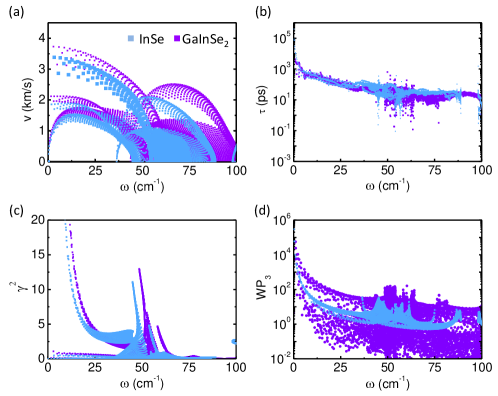
Compared to the continuously modulation of by tensile strain and rough boundary scattering, the change of due to Janus structures can keep permanent but dependents on the structures details. The phonon group velocity of monolayer GaInSe2 is larger than InSe, due to smaller atomic mass (see Fig. 4(a)). GaInSe2 occurs a breaking of mirror symmetry compared to InSe. This will lead to asymmetric chemical bonding and charge density distribution along the z-direction, which will increase bond anharmonicity [47, 48]. Fig. 4(c,d) show the square of mode Grüneisen parameter and weighted phase space , which represents the anharmonicity strength and the number of channels available for phonon scattering, respectively [49, 28]. Both and of monolayer GaInSe2 is larger than InSe, lead to stronger phonon scattering and smaller of phonon modes than that of monolayer InSe at energy zone 25 cm-1. As a result, GaInSe2 has overall higher and lower than InSe. The competition between and leads to that monolayer GaInSe2 has a comparable to that of monolayer InSe (see Fig. 1(d)).
| Type | |||||
|---|---|---|---|---|---|
| InSe | 0.181 | 0.182 | 49.21 | 5.815 | 943.3 |
| GaInSe2 | 0.160 | 0.160 | 56.76 | 6.537 | 1107.4 |
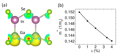
On the other side, the electron mobility of monolayer GaInSe2 was calculated based on the deformation potential theory [50]. The calculation procedure has been explained in previous work [29]. The calculated parameters involved in are shown in Table 2. The 2D effectively elastic modulus of monolayer GaInSe2 is larger than that of monolayer InSe. That is consistent with that shorter bonding length and of monolayer GaInSe2 than monolayer InSe (see Table. S1). The electron effective mass of monolayer GaInSe2 is smaller than that of monolayer InSe. The orbital analysis indicates that In- orbitals dominate the electronic states at conduction band minimum (CBM) of monolayer InSe. In contrast, the CBM of monolayer GaInSe2 is mainly composed of 5s orbital of Ga atom as well as Se- orbital (see Fig. 5(a)), due to electric potential difference arising from the charge transfering from In to Ga atoms. The Ga side of monolayer GaInSe2 experiences a tensile strain about 3.4% compared to that of monolayer GaSe, seen from the lattice constant in Table. S1. The of GaSe will decrease as the increase of tensile strain (see Fig. 5(b)). At a tensile strain of 3.4%, the is 0.144 , consistent with small of GaInSe2 (see Table. 2). Thus, monolayer GaInSe2 has a smaller and larger and deformation potential , leading to a higher than that of InSe. Meanwhile, considering its is comparable to monolayer InSe, Janus monolayer GaInSe2 is superior to monolayer InSe, monolayer In2SSe and In2SeTe in the electronic applications.
4 Conclusion
Based on the first-principles calculations, we investigated the modulation of lattice thermal conductivity of monolayer group-III chalcogenides. The room-temperature thermal conductivity of monolayer GaS, InS, GaSe and InSe is 111.0, 83.10, 58.9 and 44.9 W/(mK), respectively, which is desirable for heat dissipation of relevant devices. The heat transport of group-III chalcogenides can be well described by Slack mode and are dominated by phonon group velocity. Both acoustic branches and low-frequency optical branches have contribution to thermal transport of group-III chalcogenides. Based on that, we proposed three feasible methods to modulate the . We found that the of 2D group-III chalcogenides could be continuously decreased by tensile strain and rough boundary scattering but be increased by compressive strain. The change of due to Janus structures is permanent which depends on the structures details. Taking 2D InSe as an example, among the various Janus structure we found that the Janus monolayer GaInSe2 could keep a comparable and a higher electron mobility than monolayer InSe. Our work helps to understand of the thermal transport of 2D group-III chalcogenides and provides a guide for the thermal management in the devices based on these materials.
5 Acknowledgments
This work was supported by National Natural Science Foundation of China (No.11904312 and 11904313), the Project of Hebei Educational Department, China (No.ZD2018015 and QN2018012), the Advanced Postdoctoral Programs of Hebei Province (No.B2017003004) and the Natural Science Foundation of Hebei Province (No. A2019203507). The numerical calculations in this paper have been done on the supercomputing system in the High Performance Computing Center of Yanshan University.
References
- [1] Lei Liao, Yung-Chen Lin, Mingqiang Bao, Rui Cheng, Jingwei Bai, Yuan Liu, Yongquan Qu, Kang L. Wang, Yu Huang, and Xiangfeng Duan. High-speed graphene transistors with a self-aligned nanowire gate. Nature, 467(7313):305–308, Sep 2010.
- [2] Han Liu, Adam T. Neal, Zhen Zhu, Zhe Luo, Xianfan Xu, David Tománek, and Peide D. Ye. Phosphorene: An unexplored 2D semiconductor with a high hole mobility. ACS Nano, 8(4):4033–4041, 2014.
- [3] Xu Zhang, Xudong Zhao, Dihua Wu, Yu Jing, and Zhen Zhou. High and anisotropic carrier mobility in experimentally possible Ti2CO2 (MXene) monolayers and nanoribbons. Nanoscale, 7:16020–16025, 2015.
- [4] Jie Zou and Alexander Balandin. Phonon heat conduction in a semiconductor nanowire. J. Appl. Phys., 89(5):2932–2938, 2001.
- [5] Allon I. Hochbaum, Renkun Chen, Raul Diaz Delgado, Wenjie Liang, Erik C. Garnett, Mark Najarian, Arun Majumdar, and Peidong Yang. Enhanced thermoelectric performance of rough silicon nanowires. Nature, 451(7175):163–167, Jan 2008.
- [6] A. K. Geim. Graphene: Status and prospects. Science, 324(5934):1530–1534, 2009.
- [7] Britton W. H. Baugher, Hugh O. H. Churchill, Yafang Yang, and Pablo Jarillo-Herrero. Intrinsic electronic transport properties of high-quality monolayer and bilayer MoS2. Nano Lett., 13(9):4212–4216, 2013.
- [8] Gaoxue Wang, William J Slough, Ravindra Pandey, and Shashi P Karna. Degradation of phosphorene in air: understanding at atomic level. 2D Materials, 3(2):025011, apr 2016.
- [9] Wenjuan Huang, Lin Gan, Huiqiao Li, Ying Ma, and Tianyou Zhai. 2D layered group IIIA metal chalcogenides: synthesis, properties and applications in electronics and optoelectronics. CrystEngComm, 18:3968–3984, 2016.
- [10] Kai Xu, Lei Yin, Yun Huang, Tofik Ahmed Shifa, Junwei Chu, Feng Wang, Ruiqing Cheng, Zhenxing Wang, and Jun He. Synthesis, properties and applications of 2d layered MIIIXVI (M = Ga, In; X = S, Se, Te) materials. Nanoscale, 8:16802–16818, 2016.
- [11] Denis A Bandurin, Anastasia V Tyurnina, L Yu Geliang, Artem Mishchenko, Viktor Zólyomi, Sergey V Morozov, Roshan Krishna Kumar, Roman V Gorbachev, Zakhar R Kudrynskyi, Sergio Pezzini, et al. High electron mobility, quantum hall effect and anomalous optical response in atomically thin InSe. Nat. Nanotechnol., 12(3):223–227, Mar 2017.
- [12] Sukrit Sucharitakul, Nicholas J. Goble, U. Rajesh Kumar, Raman Sankar, Zachary A. Bogorad, Fang-Cheng Chou, Yit-Tsong Chen, and Xuan P. A. Gao. Intrinsic electron mobility exceeding cm2/(v s) in multilayer InSe FETs. Nano Lett., 15(6):3815–3819, 2015.
- [13] A. Segura, F. Pomer, A. Cantarero, W. Krause, and A. Chevy. Electron scattering mechanisms in -type indium selenide. Phys. Rev. B, 29:5708–5717, May 1984.
- [14] Shengxue Yang, Yan Li, Xiaozhou Wang, Nengjie Huo, Jian-Bai Xia, Shu-Shen Li, and Jingbo Li. High performance few-layer GaS photodetector and its unique photo-response in different gas environments. Nanoscale, 6:2582–2587, 2014.
- [15] PingAn Hu, Zhenzhong Wen, Lifeng Wang, Pingheng Tan, and Kai Xiao. Synthesis of few-layer GaSe nanosheets for high performance photodetectors. ACS Nano, 6(7):5988–5994, 2012.
- [16] Srinivasa Reddy Tamalampudi, Yi-Ying Lu, Rajesh Kumar U., Raman Sankar, Chun-Da Liao, Karukanara Moorthy B., Che-Hsuan Cheng, Fang Cheng Chou, and Yit-Tsong Chen. High performance and bendable few-layered InSe photodetectors with broad spectral response. Nano Lett., 14(5):2800–2806, 2014.
- [17] Haiyan Nan, Sijia Guo, Shuang Cai, Zhirong Chen, Amina Zafar, Xiumei Zhang, Xiaofeng Gu, Shaoqing Xiao, and Zhenhua Ni. Producing air-stable InSe nanosheet through mild oxygen plasma treatment. Semicond. Sci. Technol., 33(7):074002, 2018.
- [18] Qinghua Zhao, Riccardo Frisenda, Patricia Gant, David Perez de Lara, Carmen Munuera, Mar Garcia-Hernandez, Yue Niu, Tao Wang, Wanqi Jie, and Andres Castellanos-Gomez. Toward air stability of thin GaSe devices: Avoiding environmental and laser-induced degradation by encapsulation. Adv. Funct. Mater., 28(47):1805304, 2018.
- [19] Ching-Hwa Ho. Thickness-dependent carrier transport and optically enhanced transconductance gain in III-VI multilayer InSe. 2D Materials, 3(2):025019, 2016.
- [20] Yuanhui Sun, shulin Luo, Xin-Gang Zhao, Koushik Biswas, Songlin Li, and Lijun Zhang. InSe: a two-dimensional material with strong interlayer coupling. Nanoscale, pages 7991–7998, 2018.
- [21] P. Dey, J. Paul, N. Glikin, Z. D. Kovalyuk, Z. R. Kudrynskyi, A. H. Romero, and D. Karaiskaj. Mechanism of excitonic dephasing in layered InSe crystals. Phys. Rev. B, 89:125128, Mar 2014.
- [22] Ting Cao, Zhenglu Li, and Steven G. Louie. Tunable magnetism and half-metallicity in hole-doped monolayer GaSe. Phys. Rev. Lett., 114:236602, Jun 2015.
- [23] Hao Jin, Jianwei Li, Ying Dai, and Yadong Wei. Engineering the electronic and optoelectronic properties of InX (X = S, Se, Te) monolayers via strain. Phys. Chem. Chem. Phys., 19:4855–4860, 2017.
- [24] L Debbichi, Olle Eriksson, and S Lebègue. Two-dimensional indium selenides compounds: An ab initio study. J. Phys. Chem. Lett., 6(15):3098–3103, 2015.
- [25] Arun S Nissimagoudar, Jinlong Ma, Yani Chen, and Wu Li. Thermal transport in monolayer InSe. J. Phys.: Condens. Matter, 29(33):335702, 2017.
- [26] Tribhuwan Pandey, David S Parker, and Lucas Lindsay. Ab initio phonon thermal transport in monolayer InSe, GaSe, GaS, and alloys. Nanotechnology, 28(45):455706, 2017.
- [27] Jennifer A. Hollingsworth, Damadora M. Poojary, Abraham Clearfield, and William E. Buhro. Catalyzed growth of a metastable InS crystal structure as colloidal crystals. J. Am. Chem. Soc., 122(14):3562–3563, 2000.
- [28] Wu Li, Jesús Carrete, Nebil A Katcho, and Natalio Mingo. ShengBTE: A solver of the boltzmann transport equation for phonons. Comput. Phys. Commun., 185(6):1747 – 1758, 2014.
- [29] Wenhui Wan, Shan Zhao, Yanfeng Ge, and Yong Liu. Phonon and electron transport in janus monolayers based on InSe. J. Phys.: Condens. Matter, 31(43):435501, jul 2019.
- [30] Chen W Li, Jiawang Hong, Andrew F May, Dipanshu Bansal, Songxue Chi, Tao Hong, Georg Ehlers, and O Delaire. Orbitally driven giant phonon anharmonicity in SnSe. Nat. Phys., 11(12):1063–1069, Dec 2015.
- [31] D. T. Morelli and Slack G. A. High Thermal Conductivity Materials. Springer-Verlag New York, 2006.
- [32] Zhe Luo, Jesse Maassen, Yexin Deng, Yuchen Du, Richard P Garrelts, Mark S Lundstrom, D Ye Peide, and Xianfan Xu. Anisotropic in-plane thermal conductivity observed in few-layer black phosphorus. Nat. Commun., 6:8572, 2015.
- [33] Guangzhao Qin, Xiaoliang Zhang, Sheng-Ying Yue, Zhenzhen Qin, Huimin Wang, Yang Han, and Ming Hu. Resonant bonding driven giant phonon anharmonicity and low thermal conductivity of phosphorene. Phys. Rev. B, 94:165445, Oct 2016.
- [34] G.A. Slack. Nonmetallic crystals with high thermal conductivity. J. Phys. Chem. Solids, 34(2):321 – 335, 1973.
- [35] Chong Sun, Hui Xiang, Bo Xu, Yidong Xia, Jiang Yin, and Zhiguo Liu. Ab initio study of carrier mobility of few-layer InSe. Appl. Phys Express, 9(3):035203, 2016.
- [36] L Lindsay and DA Broido. Three-phonon phase space and lattice thermal conductivity in semiconductors. J. Phys.: Condens. Matter, 20(16):165209, 2008.
- [37] Xianghai Meng, Tribhuwan Pandey, Jihoon Jeong, Suyu Fu, Jing Yang, Ke Chen, Akash Singh, Feng He, Xiaochuan Xu, Jianshi Zhou, Wen-Pin Hsieh, Abhishek K. Singh, Jung-Fu Lin, and Yaguo Wang. Thermal conductivity enhancement in MoS2 under extreme strain. Phys. Rev. Lett., 122:155901, Apr 2019.
- [38] Atsushi Togo and Isao Tanaka. First principles phonon calculations in materials science. Scr. Mater., 108:1 – 5, 2015.
- [39] Jaroslav Fabian and Philip B. Allen. Thermal expansion and grüneisen parameters of amorphous silicon: A realistic model calculation. Phys. Rev. Lett., 79:1885–1888, Sep 1997.
- [40] Somnath Bhowmick and Vijay B. Shenoy. Effect of strain on the thermal conductivity of solids. J. Chem. Phys., 125(16):164513, 2006.
- [41] Liyan Zhu, Tingting Zhang, Ziming Sun, Jianhua Li, Guibin Chen, and Shengyuan A Yang. Thermal conductivity of biaxial-strained MoS2: sensitive strain dependence and size-dependent reduction rate. Nanotechnology, 26(46):465707, 2015.
- [42] Ruiping Li, Yingchun Cheng, and Wei Huang. Recent progress of Janus 2D transition metal chalcogenides: From theory to experiments. Small, 14(45):1802091, 2018.
- [43] San-Dong Guo. Phonon transport in Janus monolayer mosse: a first-principles study. Phys. Chem. Chem. Phys., 20:7236–7242, 2018.
- [44] A. Kandemir and H. Sahin. Janus single layers of In2SSe: A first-principles study. Phys. Rev. B, 97:155410, Apr 2018.
- [45] Yu Guo, Si Zhou, Yizhen Bai, and Jijun Zhao. Enhanced piezoelectric effect in Janus group-III chalcogenide monolayers. Appl. Phys. Lett., 110(16):163102, 2017.
- [46] Rui Peng, Yandong Ma, Shuai Zhang, Baibiao Huang, and Ying Dai. Valley polarization in Janus single-layer MoSSe via magnetic doping. J. Phys. Chem. Lett., 9(13):3612–3617, 2018.
- [47] Ai-Xia Zhang, Jiang-Tao Liu, San-Dong Guo, and Hui-Chao Li. Strain effects on phonon transport in antimonene investigated using a first-principles study. Phys. Chem. Chem. Phys., 19:14520–14526, 2017.
- [48] Xufei Wu, Vikas Varshney, Jonghoon Lee, Teng Zhang, Jennifer L. Wohlwend, Ajit K. Roy, and Tengfei Luo. Hydrogenation of penta-graphene leads to unexpected large improvement in thermal conductivity. Nano Lett., 16(6):3925–3935, 2016.
- [49] Wu Li and Natalio Mingo. Ultralow lattice thermal conductivity of the fully filled skutterudite YbFe4Sb12 due to the flat avoided-crossing filler modes. Phys. Rev. B, 91:144304, Apr 2015.
- [50] J. Bardeen and W. Shockley. Deformation potentials and mobilities in non-polar crystals. Phys. Rev., 80:72–80, Oct 1950.