Atomistic -matrix theory of disordered two-dimensional materials: Bound states, spectral properties, quasiparticle scattering, and transport
Abstract
In this work, we present an atomistic first-principles framework for modeling the low-temperature electronic and transport properties of disordered two-dimensional (2D) materials with randomly distributed point defects (impurities). The method is based on the -matrix formalism in combination with realistic density-functional theory (DFT) descriptions of the defects and their scattering matrix elements. From the -matrix approximations to the disorder-averaged Green’s function (GF) and the collision integral in the Boltzmann transport equation, the method allows calculations of, e.g., the density of states (DOS) including contributions from bound defect states, the quasiparticle spectrum and the spectral linewidth (scattering rate), and the conductivity/mobility of disordered 2D materials. We demonstrate the method by examining these quantities in monolayers of the archetypal 2D materials graphene and transition metal dichalcogenides (TMDs) contaminated with vacancy defects and substitutional impurity atoms. By comparing the Born and -matrix approximations, we also demonstrate a strong breakdown of the Born approximation for defects in 2D materials manifested in a pronounced renormalization of, e.g., the scattering rate by the higher-order -matrix method. As the -matrix approximation is essentially exact for dilute disorder, i.e., low defect concentrations () or density ( where is the unit cell area), our first-principles method provides an excellent framework for modeling the properties of disordered 2D materials with defect concentrations relevant for devices.
I Introduction
Over the past decade, there has been an explosive development in theoretical predictions Mounet et al. (2018); Haastrup et al. (2018); Olsen et al. (2019); Marrazzo et al. (2019) and experimetal fabrication of new two-dimensional (2D) materials hosting exciting electronic properties. This holds great promise for novel applications in electronics, optoelectronics, and other emerging (spin-, valley-, strain-, twist-)tronics disciplines. However, atomic disorder which degrades the material properties is still a major hindrance, and fabrication platforms that can deliver high-quality materials with low disorder concentrations are needed. Recently, there have been advances in some of the most widely studied 2D materials such as, e.g., monolayers of graphene and transition-metal dichalcogenides (TMDs), where devices based on high-quality materials encapsulated in ultra-clean van der Waals (vdW) heterostructures have shown promising electrical and optical properties Rhodes et al. (2019). Such developments are essential for the realization of quantum devices based on 2D materials Wang et al. (2018); Pisoni et al. (2018a).
The initial characterization of atomic disorder due to point defects in 2D materials often proceeds by means of scanning tunneling microscopy/spectroscopy (STM/STS) which provides valuable insight into the defect type as well as the structural and electronic properties of the defects. In, for example, graphene Rutter et al. (2007); Zhao et al. (2011); Banhart et al. (2011) and TMDs Lu et al. (2014); Zhou et al. (2016); Edelberg et al. (2019); Schuler et al. (2019a); Barja et al. (2019); Schuler et al. (2019b) this has been useful for the identification of the most common types of defects as well as probing for bound defect states which lead to strong modifications of the electronic properties of the pristine material. In addition, measurements of quasiparticle interference in various 2D materials Rutter et al. (2007); Brihuega et al. (2008); Mallet et al. (2012); Chen et al. (2012); Liu et al. (2015); Yankowitz et al. (2015); Kiraly et al. (2017); Dombrowski et al. (2017); Jolie et al. (2018), i.e., spatial ripples in the local density of states (LDOS) in the vicinity of a defect, is a direct fingerprint of the defect-induced scattering processes which may govern the electron dynamics and limit the electrical and optical performance of materials at low temperatures. Theoretical methods which can supplement such experiments in predicting the impact of defects on the electron dynamics are of high value for the understanding of electrical and optical properties of new materials.
In this work, we introduce an atomistic first-principles method for modeling the electronic properties of disordered 2D materials. Our method is based on realistic density-functional theory (DFT) calculations of the defect scattering potential and matrix elements, in combination with the -matrix formalism Rammer (1998); Bruus and Flensberg (2004) for the description of the interaction with the random disorder potential. From the disorder-averaged Green’s function (GF), accurate descriptions of experimentally relevant quantities such as, e.g., the density of states, in-gap bound and resonant quasibound defect states, spectral properties, and the disorder-induced quasiparticle scattering rate/lifetime can be obtained. Furthermore, using the -matrix scattering amplitude in the calculation of the momentum relaxation time in the Boltzmann transport equation allows for theoretical predictions of the disorder-limited low-temperature conductivity/mobility as well as its dependence on the Fermi energy (carrier density). This is thus complementary to our previous first-principles -matrix study of the LDOS and quasiparticle interference in 2D materials Kaasbjerg et al. (2017).
In comparison with analytic and tight-binding based -matrix studies of defects in, e.g., graphene Pereira et al. (2006, 2008); Hu et al. (2008); Peres et al. (2006); Wehling et al. (2010); Ducastelle (2013); Irmer et al. (2018); Kot et al. (2018) and black phosphorus Zou et al. (2016), our first-principles method permits for parameter-free modeling of realistic defects in disordered materials. It furthermore goes beyond other first-principles studies of defects and their transport-limiting effects based on the Born approximation Evans et al. (2005); Lordi et al. (2010); Fedorov et al. (2013); Restrepo et al. (2014); Lu et al. (2019a), which we here demonstrate breaks down for point defects in 2D materials. The first-principles -matrix method introduced in this work is therefore of high relevance for the further development of first-principles transport methodologies with high predictive power Zhou and Bernardi (2016); Gunst et al. (2016); Sohier et al. (2018); Poncé et al. (2018); Lu et al. (2019a); Poncé et al. (2020); Lu et al. (2019b).
The details of our method which is implemented in the GPAW electronic-structure code Mortensen et al. (2005); Larsen et al. (2009); Enkovaara et al. (2010) are described in Secs. II and III. In Secs. IV and V, we demonstrate the power of our method on a series of timely problems in disordered monolayers of TMDs and graphene. For the TMDs MoS2 and WSe2 with vacancies and oxygen substitutionals, we analyze (i) bound and quasibound defect states, respectively, in the gap and in the bands, (ii) the linewidth in the quasiparticle spectrum, the energy dependence of the scattering rate in the valleys, and the complete suppression of intervalley scattering by the spin-orbit splitting and a symmetry-induced selection rule Kaasbjerg et al. (2017), and (iii) a prediction of unconventional transport characteristics in -type WSe2 with a mobility that decreases with increasing Fermi energy. In graphene we focus on vacancies and nitrogen substitutionals and examine (i) the position of quasibound defect states on the Dirac cone, (ii) their signature in the quasiparticle spectrum and the presence (absence) of a band-gap opening for sublattice asymmetric (symmetric) defect configurations, and (iii) the pronounced electron-hole asymmetry in the transport characteristics induced by strong resonant scattering.
An important finding of this work is that the Born approximation breaks down for point defects in both TMDs and graphene, and hence most likely also in other 2D materials. While it is well-known that the description of quasibound states and resonant scattering in graphene is beyond the Born approximation, our finding that it severely overestimates the disorder-induced scattering rate in the 2D TMDs by up to several orders of magnitude is remarkable, and only emphasizes the high relevance of a first-principles -matrix approach for the modeling of disordered 2D materials.
II Atomistic defect potentials
We start by introducing an atomistic first-principles method for the calculation of the single-defect (or impurity) potential and its matrix elements which are the basic building block in the diagrammatic -matrix formalism for disordered systems outlined in Sec. III. The method is analogous to the method for calculating the electron-phonon interaction Kaasbjerg et al. (2012a, b, 2013), and is based on DFT within the projector augmented-wave (PAW) method Blöchl (1994), an LCAO supercell representation of the defect potential, and is implemented in the GPAW electronic-structure code Mortensen et al. (2005); Larsen et al. (2009); Enkovaara et al. (2010).
In this work, we restrict the considerations to nonmagnetic spin-diagonal defects in which case the defect potential for a defect of type takes the form
| (1) |
where is the scalar spin-independent defect potential and is the identity operator in spin space. We thus neglect defect-induced changes in the spin-orbit interaction, which are, in general, small relative to the spin-independent potential. The spin dependence is, of course, important for spin relaxation and spin-orbit scattering, but this is outside the scope of the present work.
Here, the spin-diagonal defect potential is defined as the change in the microscopic crystal potential induced by the defect, and is obtained from DFT as the difference in the crystal potential between the lattice with a defect and the pristine lattice, i.e.
| (2) |
The two potentials have contributions from the atomic cores (ions), which define the overall potential landscape in the lattice, as well as from the valence electrons which describe interactions between the valence electrons at a mean-field level (see Sec. II.2 below). The defect potential in Eq. (2) thus carries information about (i) the defect-induced lattice imperfection (e.g., vacancy, substitutional, or impurity atom), and (ii) the electronic relaxation in the vicinity of the defect. Both are important for a quantitative description of the defect potential.
In practice, the defect potential is expressed in a basis of Bloch states of the pristine lattice, where is the band index, st Brillouin zone (BZ) is the electronic wave vector, and is the spin index. For brevity, we combine in the following the band and spin indices in a composite “band” index. The matrix elements of the defect potential becomes
| (3) |
where as a consequence of the spin-orbit mixing of up and down spin () in the Bloch states, the matrix elements, in general, have contributions from both spin components in spite of the fact that the defect potential itself is spin-diagonal.
The following two subsections summarize our DFT-based supercell method for the calculation of the defect matrix elements. The two main technical aspects of the method concern (i) the representation of the defect potential in an LCAO basis, and (ii) the calculation of the defect potential in the PAW formalism Blöchl (1994).
II.1 LCAO supercell representation
The numerical evaluation of the defect matrix element in Eq. (II) is based on an LCAO expansion of the Bloch functions of the pristine lattice, , where is a composite atomic () and orbital index () and
| (4) |
are Bloch expansions of the spin-independent LCAO basis orbitals , where is the number of unit cells in the lattice and , , is the lattice vector to the ’th unit cell with denoting the primitive lattice vectors.
Inserting in the expression for the matrix element in Eq. (II), we find
| (5) |
where the factor of stems from the normalization of the Bloch sum in Eq. (4) to the lattice, the last factor in the second equality is the LCAO representation of the defect potential illustrated in Fig. 1, and the sums run over the cells in the lattice.
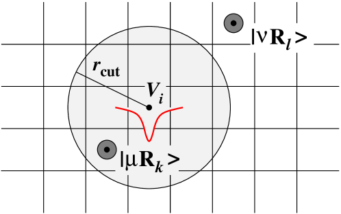
In practice, the defect potential is calculated in a finite supercell constructed by repeating the primitive unit cell times in the direction of the ’th primitive lattice vector, and with the defect site located at the center. Due to periodic boundary conditions in the in-plane directions, the supercell must be chosen large enough that defect sites in neighboring supercells do not interact. In the direction perpendicular to the material plane, the cell boundaries are imposed with Dirichlet boundary conditions, which ensures a common reference for the two potentials on the right-hand side of Eq. (2) and avoids spurious interactions between repetitions of the defect in the perpendicular direction.
In order to impose an isotropic range of the defect potential, matrix elements involving LCAO basis functions located beyond a cutoff distance from the defect site are zeroed, i.e.,
| (6) |
where is the center of the LCAO orbital at the atomic site in unit cell .
Once the LCAO representation of the defect potential in the supercell has been obtained, the defect matrix elements can be evaluated efficiently at arbitrary vectors using Eq. (II.1).
It should be noted that the LCAO procedure for the calculation of the defect matrix elements outlined here, bears close resemblance to methods based on Wannier functions Giustino et al. (2007); Lu et al. (2019b). However, the use of a fixed LCAO basis has the advantage that the additional step for the generation of the Wannier functions, which is not always trivial, is avoided.
II.2 PAW method
In the PAW formulation to DFT Blöchl (1994), the basic idea is to transform the all-electron Hamiltonian, whose eigenstates oscillate strongly in the vicinity atomic cores, into an auxiliary Hamiltonian with smooth pseudo eigenstates , thereby eliminating the numerical complications associated with an accurate description of rapidly varying functions.
The physically relevant all-electron wave functions and the auxiliary pseudo-wave functions are connected via the transformation defined as
| (7) |
where the terms in the sum over atomic sites , respectively, add and subtract expansions of the all-electron and pseudo-wave functions inside so-called augmentation spheres centered on the atoms. Here, are the correct all-electron wave functions inside the augmentation spheres, and the pseudo partial waves and projector functions are constructed to obey the completeness relation . This ensures the orthogonality of the all-electron wave functions,
| (8) |
via the operator .
Likewise, the all-electron matrix elements of the defect potential can be expressed as a matrix element of a transformed operator with respect to the smooth wave functions , i.e.,
| (9) |
where the transformed operator in the last line is given by
| (10) |
and the atomic coefficients are defined as
| (11) |
The last line in Eq. (II.2) holds for local operators and furthermore assumes that the bases are complete and that the atomic augmentation spheres do not overlap. However, in practical PAW calculations, finite bases and small overlaps between different augmentation spheres can be tolerated without substantial loss of accuracy.
The transformed operator, which incorporates the full details of the potential due to the all-electron density (frozen core + valence electrons), can be expressed as
| (12) |
where is the effective potential given by the sum of the electrostatic Hartree potential (including the potential due to the atomic cores) and the exchange-correlation potential , and the last term is the all-electron corrections given by the atomic coefficients defined in Eq. (11). Full PAW expressions for and can be found in, e.g., Ref. Enkovaara et al., 2010.
In the defect potential in Eq. (2), the two contributions to the potential in Eq. (12) describe, respectively, perturbations in the crystal potential and atomic-core states on the defect. The latter term can be regarded as the PAW analog of a Löwdin downfolding of atomic defect states onto the Bloch functions Irmer et al. (2018).
II.3 Examples
In this section, we show examples of matrix elements for the defects in 2D TMDs and graphene studied in Secs. IV and V below.
In order to relate the DFT-calculated matrix elements (which have units of energy) to the impurity strength of the -function potential in continuum descriptions of defects, , it is instructive to rewrite the matrix element as
| (13) |
where the definition of in the first step follows trivially from Eq. (II.1), and in the second step we have used that , where and are, respectively, the sample and unit-cell area. In the last equation, has units of like the impurity strength above. In the following, the first symbol in Eq. (13) is used interchangeably for the different matrix elements.
II.3.1 Defects in 2D TMDs
The semiconducting TMD monolayers are some of the most well-studied 2D materials in terms of electrical, optical, and structural properties. This includes numerous STM/STS studies of their atomic defects, showing that the most common types of defects are monovacancies Zhou et al. (2013); Lin et al. (2014); Hong et al. (2015); Komsa et al. (2012); Liu et al. (2013); Noh et al. (2014); Komsa and Krasheninnikov (2015); Zhang et al. (2017); Jiang et al. (2018); Guguchia et al. (2018); Moody et al. (2018); Schuler et al. (2019a), oxygen substitutionals Zheng et al. (2019); Barja et al. (2019); Schuler et al. (2019b); Aghajanian et al. (2019), i.e., an oxygen atom substituting a chalcogenide atom, and antisite defects Guguchia et al. (2018); Edelberg et al. (2019). The variability in the predominant defect type stems from the different fabrication techniques Rhodes et al. (2019), where so far CVD/CVT yield rather low material quality in comparison to recent flux-grown materials Edelberg et al. (2019); Luo et al. (2018) with defect densities as low as – cm-2.
In this work, we focus on atomic monovacancies and oxygen substitutionals. In our DFT calculations of the defect supercell, we find in agreement with previous works Komsa et al. (2012); Liu et al. (2013); Noh et al. (2014); Komsa and Krasheninnikov (2015) that structural relaxation around the defect site is minor and is therefore disregarded here.
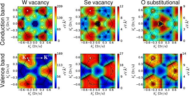
Figure 2 summarizes the defect matrix elements in 2D WSe2 for W and Se monovacancies (VW,Se) as well as oxygen substitutionals (OSe). The plots show the absolute value of the spin- and band-diagonal matrix element in the valence (bottom row) and conduction (top row) bands, with the initial state of the matrix element fixed to which is the position of the band edges in most of the semiconducting monolayer TMDs Nguyen et al. (2019). The intravalley and intervalley matrix elements are indicated with, respectively, a small and a large arrow in the lower left plot.
Overall, the matrix elements exhibit a nontrivial wave-vector dependence as a function of . Only in the vicinity of the high-symmetry points are the matrix elements characterized by regions with trigonal symmetry where a relatively constant value is attained. The magnitude of the intravalley and intervalley matrix elements for the W vacancy are about an order of magnitude larger than the matrix elements for the Se vacancy and O substitutional. This can be understood from the fact that the Bloch states are dominated by the transition-metal orbitals Xiao et al. (2012), and therefore have a larger overlap with defects on the transition-metal site compared to defects on the chalcogenide sites. On the contrary, the matrix elements for the Se vacancy and O substitutional resemble each other, indicating that the two types of defects will have similar impact on the electronic properties of WSe2.
As expected for atomic point defects, the W vacancy gives rise to both strong intravalley and intervalley matrix elements which are comparable in magnitude. On the other hand, the matrix elements for the Se vacancy and O substitutional, as well as the valence-band matrix element for the W vacancy, show a highly unconventional feature; their intervalley matrix elements are strongly suppressed and vanishes identically between the two high-symmetry points. This is in spite of the fact that we here consider the spin-conserving matrix element where the spin is the same for the two Bloch functions in the matrix element in Eq. (II). That is, this feature is unrelated to the SO splitting of the bands Zhu et al. (2011); Kośmider et al. (2013). In a recent work Kaasbjerg et al. (2017), we have shown that this originates from the symmetry of the defect sites together with the valley-dependent orbital character of the Bloch functions Kaasbjerg et al. (2017), which give rise to a symmetry-induced selection rule that makes the valence and conduction band intervalley matrix elements vanish identically, except for defects on the transition-metal site where it only vanishes in the valence band.
Another important selection rule is the one imposed by time-reversal symmetry on the intervalley matrix element between states of opposite spin at the and points,
| (14) |
where . Note that this holds even in the presence of spin-orbit coupling in the defect potential which does not break time-reversal symmetry.
II.3.2 Graphene
Graphene is a host of a large variety of defects ranging from vacancies and lattice reconstructions like, e.g., Stone-Wales defects, to adatoms and substitutional atoms involving alkali-metal, halogen, and other nonmetallic atoms, or molecules Banhart et al. (2011); Rhodes et al. (2019). In this work, we restrict the considerations to single carbon vacancies Chen et al. (2009); Ugeda et al. (2010); Chen et al. (2011); Mao et al. (2016) and nitrogen substitutionals Zhao et al. (2011); Usachov et al. (2011); Joucken et al. (2012).
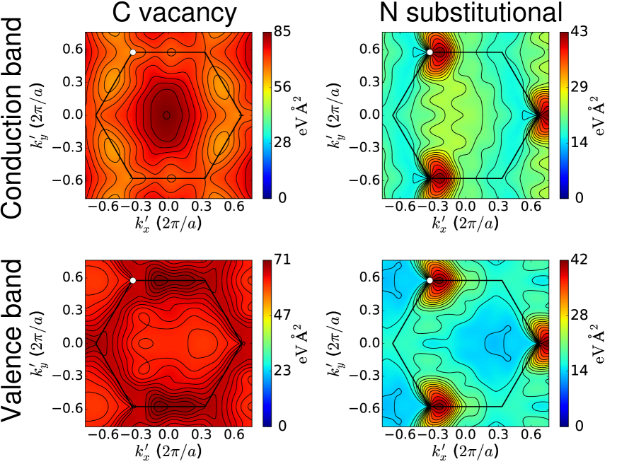
In Fig. 3 we show the valence and conduction-band matrix elements for a carbon vacancy (left) and a nitrogen substitutional (right). In contrast to the matrix elements for the TMDs in Fig. 2, there are no selection rules on the matrix elements for vacancies and substitutionals in graphene. Consequently, their matrix elements show less variation as a function of and the intravalley and intervalley matrix elements are both significant.
It is instructive to analyze the matrix elements in Fig. 3 in terms of the standard tight-binding (TB) model for vacancies Pereira et al. (2006); Wehling et al. (2007); Pereira et al. (2008); Ducastelle (2013); Duffy et al. (2016); Ruiz-Tijerina and Dias da Silva (2016); Kot et al. (2018) and substitutional atoms Lherbier et al. (2008); Lambin et al. (2012); Lherbier et al. (2013), where the defect is often described by a change in the onsite energy of the defect site. In the sublattice (pseudospin) basis, the defect potential can therefore be expressed as
| (15) |
where , , are Pauli matrices ( denotes the identity matrix) in the pseudospin basis, and is for defects on the and sublattice, respectively.
For wave vectors in the vicinity of the points, the graphene TB Hamiltonian can be approximated by the Dirac model, , where is the valley index, and , with eigenstates and eigenenergies , where is the band index for the conduction () and valence () bands, respectively.
Without loss of generality, we now for simplicity consider a defect on an site. Performing a unitary transformation to the eigenstate basis, the matrix elements of the defect potential in Eq. (15) become
| (16) |
which are independent on the wave vectors and band indices , and thus correspond to identical intravalley and intervalley as well as intraband and interband couplings.
For the vacancy defect in Fig. 3, Eq. (16) is seen to be a reasonable approximation in the vicinity of the points. From the value of the intra- and intervalley matrix elements, , we find via Eq. (13) that the energy shift at the vacancy site is eV (). The positive sign can be attributed to the missing attractive core potential as well as unpaired electrons left at the vacancy site which yield an overall repulsive defect potential in Eq. (12).
For the N substitutional in Fig. 3, the different values of the intra- and intervalley matrix elements as well as the anisotropy of the intravalley matrix element indicate that Eq. (16) is a less good approximation. This is due to the fact that substitutional nitrogen donates a fraction of an electron to the graphene lattice and thereby ends up as a positively charged impurity characterized by a strong intravalley matrix element Hwang et al. (2007). The defect potential due to chemical substitutionals therefore presents both short range (since there is a substantial onsite chemical energy shift) as well as some long-range features Lherbier et al. (2008). In Sec. V below, we find that an average value of eV ( ), where the minus sign is due to the partially positively charged N substitutional, yields good agreement with our full DFT-based results.
III -matrix formalism
In this section, we introduce the -matrix formalism Rammer (1998); Bruus and Flensberg (2004) for the description of (i) a single isolated defect at with defect potential , and (ii) disordered systems with a random configuration of defects and total disorder potential where denotes the positions of defects of type . The latter case is the main focus of this work.
III.1 Single defects
The situation of a single isolated defect in an otherwise perfect infinite lattice is relevant for, e.g., STM/STS studies which probe the LDOS in the vicinity of the defect site which can be obtained as
| (17) |
where is the real-space representation of the Green’s function (GF; all Green’s functions are assumed to be retarded in this work).
For the single-defect problem, the exact GF can be expressed in terms of the matrix which describes scattering off the defect to infinite order in the defect potential, , where is the GF of the pristine lattice. In the basis of the Bloch states of the pristine lattice, the GF becomes
| (18) |
where , and
| (19) |
Here, are the matrix elements of the defect potential in Eq. (II) and the sum over st BZ is over virtual intermediate states. In contrast to , the matrix is, in general, not Hermitian.
Given the GF in Eq. (18), the real-space LDOS in Eq. (17) which contains information about the electronic properties of the defect can be obtained via a Fourier transform Kaasbjerg et al. (2017). For example, defect-induced bound states manifest themselves in a high LDOS intensity at energies corresponding to the bound-state energy. They arise when the matrix introduces new poles in the GF via the correction in the last term of Eq. (18). From the full matrix form of the -matrix
| (20) |
where the boldface symbols denote matrices in the band () and wave-vector () indices, the poles of the matrix are seen to appear at energies where the determinant of the matrix in the square brackets vanishes, i.e.,
| (21) |
Therefore, the positions of the bound states depend sensitively on the defect matrix elements and the band structure, and since also high-energy bands can be involved in the formation of bound states, their exact position can, in general, not be inferred from low-energy models. For in-gap bound states residing in the band gap of a semiconductor, the bound states form discrete energy levels and will be strongly localized to the defect site due to a weak interaction with the delocalized Bloch states. On the other hand, quasibound resonant state in the bands acquire a finite width and tend to be more delocalized.
III.2 Disordered systems
In disordered systems with a random configuration of defects, experimental observables are often self-averaging and must be obtained on the basis of the disorder-averaged GF. In contrast to the single-defect problem discussed above, the problem for the disorder-averaged GF cannot be solved exactly.
The disorder-averaged GF is given by the Dyson equation
| (22) |
where the disorder self-energy accounts for the interaction with the disorder potential, and introduces spectral shifts, broadening, and potentially bound defect states. As the disorder average restores translational symmetry, the GF is diagonal in . However, the matrix structure in the band and spin indices is retained, and Eq. (22) must be solved by matrix inversion.
In this work, the self-energy is described at the level of the Born and -matrix (full Born) approximations Rammer (1998); Bruus and Flensberg (2004), which apply to dilute concentrations of defects. The two self-energies are illustrated with Feynman diagrams in Fig. 4, where the individual diagrams describe repeated scattering off single defects to different orders in the scattering potential.
The -matrix self-energy in the bottom equation of Fig. 4 takes into account multiple scattering off defects to all orders in the defect potential, and is therefore exact to lowest order in the disorder concentration (or density ) where is the number of defects of type . The self-energy is given by Rammer (1998); Bruus and Flensberg (2004)
| (23) |
where is the matrix in Eq. (19), and can be expressed in terms of the -diagonal of the matrix as
| (24) |
Here, the definitions of the symbols in the two last equalities are analogous to the ones for the defect matrix elements in Eq. (13), and express the self-energy in terms of the disorder concentration or density , respectively. In the latter case, the matrix has units of .

In the Born approximation in the top equation of Fig. 4, the self-energy is truncated after the second-order term in Eq. (23), i.e.,
| (25) |
Here, the first lowest-order term given by the -diagonal matrix elements of the defect potential is purely real and gives rise to a shift of the unperturbed band energies . The second-order contribution in the last term gives the leading-order contribution to the scattering rate, or linewidth broadening, corresponding to the Fermi’s golden rule expression
| (26) |
In Sec. III.2.1 below, we discuss the -matrix generalization of this expression via the Optical theorem.
In the above, we have only considered defects of a single type . For disorder consisting of different types of defects, the disorder average involves an average over the defect types in addition to the usual average over their random positions. In the Born and -matrix approximations which neglect coherent scattering off different defect sites, this amounts to averaging over the self-energies of the different defect types, i.e.
| (27) |
where is the total number of defects, and is the fraction of defects of type . Note that this procedure does not apply to self-energies containing, e.g., diagrams with crossed impurity lines Rammer (1998); Bruus and Flensberg (2004). In the following, we omit the sum over defect types for brevity.
The difference between the Born and -matrix approximations is that the Born approximation is only valid for weak defects, while the infinite-order -matrix approximation applies to defects of arbitrary strength. As a consequence, the matrix generally renormalizes the Born results due to multiple scattering processes if the defect is not weak. The formation of bound defect states is another good example where the Born approximation fails to capture the correct physical picture described by the -matrix approximation.
Both the Born and -matrix self-energies are first order in the disorder concentration (defect sites per unit cell), and hence valid for dilute defect concentrations, (or ). To demonstrate the wide range of disorder densities where this is fulfilled in 2D materials, we consider graphene () where a disorder concentration of is equivalent to a density of . This corresponds to a rather poor material quality, why the -matrix self-energy is an excellent approximation for most experimentally relevant disorder concentrations.
At the level of the two-particle GF for the conductivity there are, however, effects not captured by the -matrix approximation even at low disorder concentrations. One well-known example is the weak-localization correction to the conductivity which arises due to interference between scattering processes at different defect sites Altshuler et al. (1980); Lee and Ramakrishnan (1985). Nevertheless, the -matrix approach presented here provides a good compromise between wide applicability and practicality for applications with realistic defects and band structures.
III.2.1 Quasiparticle spectrum and scattering
As a consequence of disorder scattering, the pristine band structure is renormalized and broadened, yielding quasiparticle (QP) states with a finite lifetime which can be probed in, e.g., ARPES. The measured spectral function is given by the diagonal elements of the GF as
| (28) |
where obeys the sum rule .
While our numerical calculations of the spectral function and DOS presented below are based on the full matrix form of the GF in Eq. (22), it is instructive to assume a diagonal form of the self-energy and GF,
| (29) |
in order to analyze the effects of disorder scattering in closer detail.
In the diagonal approximation for the GF in Eq. (29), the spectral function can in the vicinity of the QP energies given by the solution to the QP equation
| (30) |
be approximated as
| (31) |
where the QP weight is given by , and the linewidth broadening is given by the imaginary part of the self-energy,
| (32) |
evaluated at the on-shell QP energy , and where the last equality holds for the -matrix self-energy.
Via the optical theorem Rammer (1998); Bruus and Flensberg (2004), the diagonal elements of the imaginary part of the matrix can be expressed as
| (33) |
and the lifetime broadening (or scattering rate) in Eq. (III.2.1) can be brought on a form which resembles the Born expression in Eq. (26). This allows to identify the elements of the matrix as the renormalized Born scattering amplitude given by the bare matrix element . Furthermore, the optical theorem in Eq. (III.2.1) can be used to separate out the contributions to the lifetime broadening from, e.g., intravalley and intervalley scattering by splitting the sum into sums over intravalley and intervalley processes, . This may be desirable in order to extract, e.g., the disorder-limited valley lifetime.
In context of the discussion of scattering above, it is important to note that selection rules in the defect matrix elements imposed by a symmetry common to the lattice and defect potential, , are transferred to the elements of the matrix. This follows straight forwardly from the fact that the matrix transforms as the defect potential, , under such symmetry transformations. Thus, scattering processes which are forbidden by symmetry due to vanishing matrix elements in the Born approximation, are also forbidden in -matrix approximations, in spite of the fact that scattering processes in the latter case proceed via virtual intermediate states.
III.2.2 Bound defect states
When bound states appear in the single-defect problem, it is interesting to ask how they manifest themselves in the spectral function and the DOS (here defined per unit cell) of the disordered system,
| (34) |
where is the number of unit cells in the lattice. Naively, one would expect peaks at the bound-state energies of the isolated defect. To shed light on the the bound-state DOS of a dilute disordered system, we consider a situation where the single-defect GF in Eq. (18) has an in-gap bound state stemming from a pole of the matrix with energy .
To facilitate a simple analysis, we resort again to the diagonal form of the GF in Eq. (29). In this case, the self-energy is given by the diagonal elements of the matrix, which in the vicinity of the pole can be approximated as
| (35) |
where (with unit ) is the strength of the pole for a given band and point, and the positive infinitesimal ensures the correct analytic behavior of the matrix.
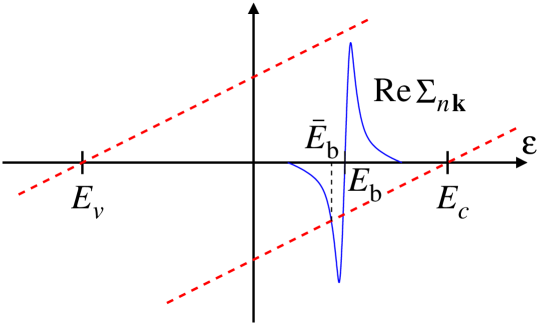
We now demonstrate how the pole of the matrix gives rise to a new bound-state pole in the disorder-averaged GF, whose energy we denote in order to distinguish it from the -matrix pole at . The bound state, being a well-defined quasiparticle of the disordered system, emerges as a new solution to the QP equation in Eq. (30) with energy as sketched graphically in Fig. 5 for states at the band edges, i.e., . Here, the generic shape of the real part of the matrix (self-energy) originates from its pole form in Eq. (35).
Expanding the self-energy around , , the in-gap GF takes the form
| (36) |
where is the contribution to the spectral weight of the bound states from the state . Note that bound states may have contributions from several bands, and by virtue of the sum-rule for the spectral function in Eq. (28), in order for the pristine bands to remain well-defined.
In the presence of bound states, the spectral function in Eq. (28) thus becomes a sum of two contributions given, respectively, by (i) Eq. (31) describing the QPs associated with the pristine bands, and (ii) the imaginary part of Eq. (36) for the bound state. Note that the bound-state solution to the QP equation may, in fact, depend on both and , such that dispersive defect bands, i.e. , may arise even though hybridization between the defects is not accounted for in the -matrix approximation. As we demonstrated in a recent work, this situation arises in, e.g., alkali-metal-decorated graphene Kaasbjerg and Jauho (2019).
The bound-state position naturally depends on the disorder concentration via Eq. (30). With the self-energy given by the pole form of the matrix in Eq. (35), it follows straight forwardly that in the limit of . This is not surprising as the limit is equivalent to setting and letting , i.e., the single-defect limit. In addition, the quasiparticle weight vanishes as , implying that the in-gap form of the imaginary part of the GF becomes
| (37) |
which is identical to the in-gap form of the imaginary part of the single-defect GF (its diagonal elements) in Eq. (18). Thus, the bound-state DOS of a dilute system approaches the single-defect DOS for as anticipated, and its weight vanishes as compared to the DOS of the pristine lattice. At higher disorder concentrations (but still ), the graphical solution of Eq. (30) in Fig. 5 indicates that the GF pole drifts away from the -matrix pole at .
III.2.3 Transport
At low temperatures where electron-phonon scattering is frozen out, the longitudinal conductivity is often limited by the intrinsic disorder of the material. Within the framework of Boltzmann transport theory, the disorder-limited longitudinal conductivity can be obtained from the current density,
| (38) |
where is the charge of the carriers, is the band velocity, and is the deviation of the distribution function away from the equilibrium Fermi-Dirac distribution, , to first order in the applied field .
The deviation function is given by the linearized Boltzmann equation which for elastic disorder scattering in a multiband system takes the form
| (39) |
where
| (40) |
is the transition rate in the -matrix approximation, which follows from the optical theorem in Eq. (III.2.1).
In Appendix A we outline a least-square method for the solution of the Boltzmann equation (39) on general -point grids and with first-principles inputs for the band structure, band velocities, and elastic scattering rate. The method does not rely on any assumptions about the functional form of the deviation function or a relaxation-time approximation. Other approaches for the solution of the BE based on first-principles input for inelastic electron-phonon scattering have been discussed in the literature Zhou and Bernardi (2016); Gunst et al. (2016); Sohier et al. (2018). Our method in Appendix A was recently applied in calculations of the transport properties of Li-doped graphene within a TB description of the graphene bands and the Li-induced carrier scattering Khademi et al. (2019).
In the calculations presented in this work, we restrict the discussion to transport involving a single band (spin-degenerate or spin-orbit split), and furthermore assume that the band structure is isotropic with a constant effective mass (or Fermi velocity in the case of graphene), which is a good approximation for the transport-relevant energy range close to the band edges. In this case, the conductivity can be expressed in terms of the relaxation time given by the -matrix scattering amplitude as
| (41) |
where is the scattering angle. The only difference between the QP scattering rate in Eqs. (III.2.1) and (III.2.1) and the inverse transport relaxation time is the factor in the square brackets, which accounts for the fact that the transport is insensitive to small-angle scattering while the QP lifetime is equally sensitive to all scattering processes. For isotropic scattering, the two scattering times become identical as the angular integral of the term vanishes.
With the above-mentioned assumptions and considering the low-temperature limit (), the conductivity in Eq. (38) simplifies to the well-known Drude form given by
| (42) |
in, respectively, a 2D semiconductor and graphene, where is the carrier density and is the density of states. In combination with first-principles calculations of the -matrix transport relaxation time in Eq. (III.2.3), these expressions provide a simple and accurate framework for calculating the low-temperature conductivity in disordered 2D materials.
III.3 Numerical and calculational details
The calculation of the matrix in Eq. (19) is the most demanding step in the evaluation of the above-mentioned quantities. Rather than solving the equation by direct matrix inversion as in (20), it is numerically more stable to recast it as a system of coupled linear equation (one set of coupled equations for each column in and ),
| (43) |
and solve it with a standard linear solver. This requires one factorization followed by a matrix-vector multiplications and scales as where denotes the matrix dimension.
The calculation of the matrix must be checked for convergence with respect to (i) the BZ sampling with points on either uniform BZ grids or nonuniform grids with a higher density of grid points in the vicinity of important high-symmetry points (see Fig. 6), and (ii) the number of bands included in the calculation of the matrix. In general, we have found that the convergence of the position of bound defect states in the gap of 2D semiconductors requires a large number of bands () starting from the bottom of the spectrum and up to high energies, while only a moderate sampling () is required. On the other hand, the linewidth broadening in Eq. (III.2.1) [and Eq. (III.2.1)] requires only a few bands (–) (as long as there are no bound states in the bands), but a dense -point grid () in order to sample the constant-energy surface on which the quasiparticle scattering takes place. In the case of graphene, quasibound resonant states are inherent to the Dirac cone dispersion, and hence both the the resonant state and the scattering rate can be calculated with a dense -point sampling including only a few bands.
With the above-mentioned number of bands and -point samplings, the dimension of the matrices in Eqs. (43) becomes –. With the matrix elements represented as 128-bit complex floating-point numbers, the memory requirement for each of the dense complex matrices in Eq. (43) becomes – GBs. To tackle the large matrix dimensions in the solution of the matrix equation in Eq. (43), we exploit the automatic openMP multithreading of the LAPACK linear solvers.
In the calculation of the DOS in Eq. (34), a very fine -point sampling is needed to converge the DOS of the bands near the band edges. We therefore (i) first calculate the difference between the DOS of the disordered and pristine materials on a coarse -point grid (in order to include enough bands to capture bound states), and (ii) subsequently add to the DOS of the pristine material obtained on a fine -point grid. In this way, we avoid spiky artifacts in the DOS of the bands due to insufficient -point sampling, while at the same time capturing potential defect states in the bands.
For the results presented in the following sections, the band structures and defect matrix elements have been obtained with the GPAW electronic-structure code Mortensen et al. (2005); Larsen et al. (2009); Enkovaara et al. (2010), using DFT-LDA within the projector augmented-wave (PAW) method, a DZP LCAO basis, and including spin-orbit interaction Olsen (2016). The parameters used in the individual calculations are listed in the figure captions.
IV Disordered 2D TMDs
The experimental consensus on the prevalent types of defects in the 2D TMDs (see Sec. II.3.1) has led to numerous theoretical DFT studies of their structural and electronic properties Noh et al. (2014); Komsa et al. (2014); Carvalho and Neto (2014); Komsa and Krasheninnikov (2015); Haldar et al. (2015); Krivosheeva et al. (2015); Pandey et al. (2016); Kaasbjerg et al. (2017); Khan et al. (2017); Pizzochero and Yazyev (2017). On the other hand, first-principles calculations of the impact on electron dynamics in disordered 2D TMDs remain few Refaely-Abramson et al. (2018); Kaasbjerg et al. (2019). In the following subsections, we analyze in detail the electronic (DOS and quasiparticle spectrum) and transport (conductivity and mobiliy) properties.
IV.1 DOS and in-gap bound states
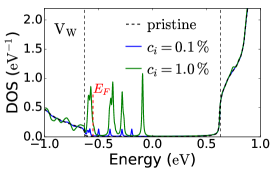
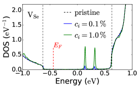
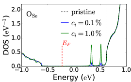
We start by discussing the impact of defects on the DOS, and in particular the defect-induced in-gap states observed in various STM/STS experiments Lu et al. (2014); Zhou et al. (2016); Edelberg et al. (2019); Schuler et al. (2019a); Barja et al. (2019); Schuler et al. (2019b). Figure 7 shows the DOS for disordered MoS2 (top) and WSe2 (bottom) with different types of defects. The dashed vertical lines mark the position of the valence and conduction band edges (black) as well as the Fermi energy (; red dashed line). All the defects, in particular transition-metal vacancies, introduce a series of defect-localized in-gap states at positions in good agreement with previously reported DFT supercell calculations Noh et al. (2014); Li et al. (2016); Khan et al. (2017); Refaely-Abramson et al. (2018).
Our results in Fig. 7 show that some of the orbitally-degenerate bound states are subject to a notable spin-orbit induced spin splitting. This is also in agreement with previous supercell calculations of defect-induced in-gap states taking into account spin-orbit interaction Li et al. (2016); Refaely-Abramson et al. (2018); Schuler et al. (2019a). In MoS2, the splitting is of the order of meV for the two states above the Fermi energy and the two top states, whereas a significantly larger splitting of meV is observed for the unoccupied and states in WSe2. It should be noted that this effect is captured in spite of the fact that we here consider spin-independent defect potentials, i.e. the spin-orbit interaction enters only through the unperturbed band structure.
It is interesting to note that most of the considered defects introduce both occupied and unoccupied in-gap states occur, except for the and defects in WSe2 which only introduce unoccupied in-gap states. For all the other defects, the shallow occupied states above the valence-band edge act as hole traps in the -doped (gated) materials. The converse holds for the unoccupied in-gap states which act as deep electron traps in the -doped materials. As we have recently demonstrated, the charging of the defect sites resulting from such carrier trapping has detrimental impact on the transport properties of gated 2D TMDs Kaasbjerg et al. (2019).
In addition to in-gap bound state, defects may also introduce quasibound states inside the bands as predicted in, e.g., MoSe2 and WS2 Refaely-Abramson et al. (2018); Schuler et al. (2019a). As witnessed by the curves in Fig. 7 which show pronounced deviations from the pristine DOS inside the bands, this seems to be the case also in MoS2 and WSe2. However, we find that some of these features are artifacts from the procedure we have used to calculate the DOS in the bands of the disordered system (see Sec. III.3 above). Only the features in the valence band for Mo vacancies in MoS2 ( meV below the band edge), W ( meV below the band edge) and Se vacancies ( meV below the band edge) in WSe2 correspond to true quasibound states. As their positions are reasonably far away from the band edges, resonant scattering off the quasibound states can be neglected in calculations of the disorder-limited transport properties Kaasbjerg et al. (2019). By contrast, both bound and quasibound defect states have been demonstrated to alter the optical properties of 2D TMDs by binding the excitons in the defect states Zhang et al. (2017); Moody et al. (2018); Refaely-Abramson et al. (2018); Zheng et al. (2019).
IV.2 Spectral function and quasiparticle scattering
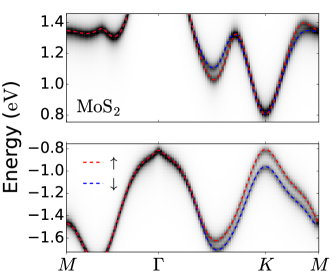
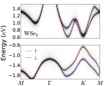
In Fig. 8, we show the valence and conduction band spectral functions (grayscale intensity plots) for disordered MoS2 and WSe2 with a concentration of, respectively, Mo and Se vacancies together with the unperturbed band structure of the pristine materials (dashed lines). Although our DFT calculations indicate that the direct and indirect band gaps in MoS2 and WSe2 are almost identical, and that the band gap in some cases is indirect Zhang et al. (2015), recent microARPES experiments have given conclusive evidence that the band gap in monolayers of the semiconducting TMDs with and is direct Nguyen et al. (2019).
Overall, the spectral functions overlap almost perfectly with the unperturbed band structures, indicating that disorder-induced renormalization of the bands is small at in the -matrix approximation. This is in stark contrast to the Born approximation (not shown), where the first term in Eq. (25) given by the bare defect matrix element gives rise to a giant shift of the bands. In the -matrix approximation, this shift is strongly renormalized by the matrix inverse on the right-hand side of Eq. (20).
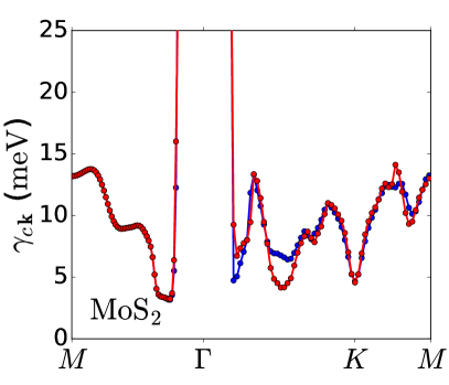
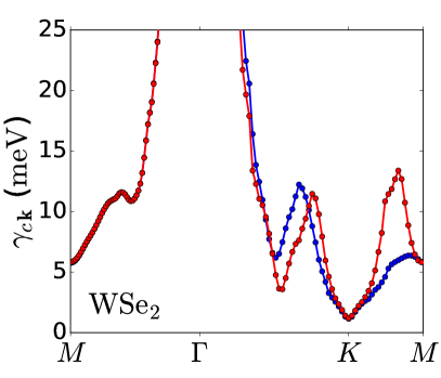
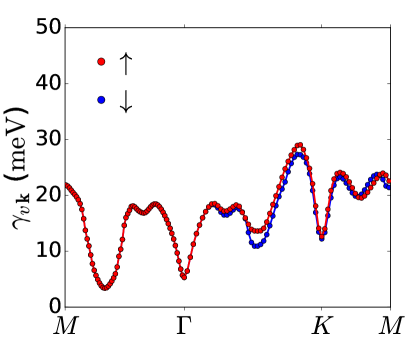
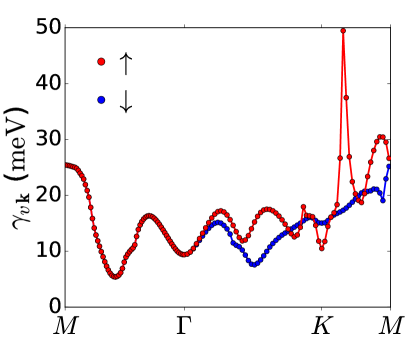
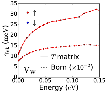
The quasiparticle lifetime given by the broadening of the spectral function is difficult to infer from Fig. 8 due to the numerical broadening . In Fig. 9 we therefore show the linewidth broadenings obtained directly from the on-shell self-energy via Eq. (III.2.1). Overall, the linewidths show a pronounced dependence on with multiple peaks and dips along the considered path in the BZ. The strong increase in the linewidth in the vicinity of the point in the conduction bands (top plots) is due to overlap with higher-lying bands outside the energy range shown in Fig. 8. The sharp peak in the linewidth along the - path in the lower right plot is due to resonant scattering off the quasibound defect state introduced by the Se vacancy in the valence band. For the defect concentration considered here, the overall magnitude of the disorder-induced linewidth is comparable to the phonon-induced linewidth at elevated temperatures Molina-Sánchez et al. (2016).
In the and valleys close to the band edges, the linewidths show characteristic dips with a particularly sharp shape. To analyze these features in closer detail, we show in Figs. 10 and 11 the linewidths for the spin up and down bands in valley of, respectively, the conduction band of MoS2 (Mo and S vacancies) and the valence band of WSe2 (W and Se vacancies) as a function of the band energy (measured with respect to the band edges) instead of . In the two figures, the left columns show a comparison between the Born [Eq. (26)] and -matrix approximations, whereas the right columns show the contributions to linewidth from intravalley and intervalley scattering. Due to the large spin-orbit splitting in the valence band of WSe2, only the linewidth for the spin-up band appears in Fig. 11. Note that different -point samplings have been used in the two figures, hence the difference in energy resolution.
In Figs. 10 and 11, the sharp dips in the linewidths in Fig. 9 mentioned above are manifested in a strong energy dependence of the -matrix linewidths close to the band edges. For comparison, the linewidths in the Born approximation exhibit a weaker energy dependence which can be traced back to the almost constant matrix elements in Fig. 2 inside the valleys, implying that the Born linewidth given by Eq. (26) to a good approximation becomes proportional to the DOS in the valleys. The energy dependence of the Born linewidths therefore reflects the gradual increase in the DOS in Fig. 7 at the band edges. On the contrary, the sharp drop in the -matrix linewidths at the band edges is a consequence of higher-order renormalization of the Born scattering amplitude by multiple scattering processes. This makes the -matrix amplitude strongly energy dependent, and can modeled quantitatively with a simple analytic -matrix model as we have demonstrated in Ref. Kaasbjerg et al., 2019.
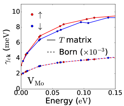

Another consequence of the higher-order renormalization is a strong reduction of the scattering amplitude between the Born and -matrix approximations. This is evident from Fig. 10 where the former overestimates the scattering rates up to three orders of magnitude. The reduction is largest for vacancies which are strong defects (cf. the matrix elements in Fig. 2) for which the matrix leads to a giant renormalization of the Born scattering amplitude. For the weaker centered defects (vacancies and substitutional atoms), the matrix elements in Fig. 2 are smaller, but still large enough for the matrix to yield a nonnegligible renormalization of the scattering amplitude. These observations point to a concomitant breakdown of the Born approximation and stress the importance of a -matrix description of atomic defects in 2D TMDs.


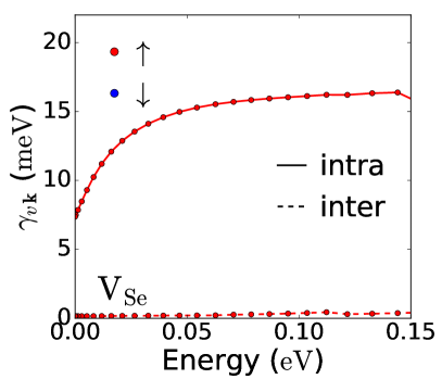
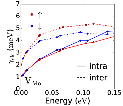
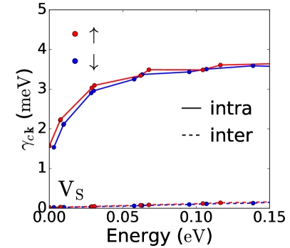
In the plots in the right columns of Figs. 10 and 11, we have separated out the contributions to the linewidth broadening from intravalley (solid lines) and intervalley (dashed lines) scattering. Interestingly, the plots show that while the intravalley and intervalley contributions are of the same order of magnitude for Mo vacancies in MoS2, the intervalley contribution is negligibly small for S vacancies as well as W and Se vacancies in WSe2. In the almost spin-degenerate conduction band of MoS2 Kośmider et al. (2013), this is related to the symmetry-induced selection rules for the intervalley matrix elements discussed in Sec. II.3.1 and Ref. Kaasbjerg et al., 2017, which strongly suppress intervalley scattering by -centered defects in 2D TMDs. In the valence band of WSe2, this as well as the large and opposite spin-orbit splitting in the valleys Zhu et al. (2011), suppress intervalley scattering. Long valley lifetimes exceeding hundreds of ps are therefore achievable even in highly disordered 2D TMDs if -centered defects can be eliminated.
Our finding for the suppression of intervalley scattering by chalcogen-centered defects is also relevant for studies of weak localization/antilocalization in 2D TMDs Lu et al. (2013); Ochoa et al. (2014); Schmidt et al. (2016); Ilić et al. (2019); Chu et al. (2019), where, e.g., S vacancies in -doped MoS2 have often been mentioned as a source pronounced intervalley scattering Schmidt et al. (2016); Ilić et al. (2019); Chu et al. (2019). As we have demonstrated here, this is not the case and intervalley scattering must instead be attributed to the existence of other point defects.
IV.3 Transport
In studies of the disorder-limited transport properties of 2D TMDs, it is important to consider the fact that defect-induced in-gap states can trap holes or electrons as extrinsic carriers (i.e., gate induced) are introduced into the bands. This holds, respectively, for occupied in-gap states in -doped as well as unoccupied in-gap states in -doped samples, and results in charging of the defect sites. A description of such charging effects within the framework of our method in Sec. II is beyond the scope of this work. Based on a simple model, we recently demonstrated that the charge-impurity scattering resulting from charging of defects has detrimental consequences for the carrier mobility in 2D TMDs Kaasbjerg et al. (2019), and is therefore unfavorable in order to realize high-mobility TMD samples.
In the following, we focus on cases where defect charging is not expected. As witnessed by Fig. 7, this situation is encountered in -doped WSe2 with Se vacancies or O substitutionals which only introduce unoccupied in-gap states above the intrinsic Fermi level. Upon doping the material, i.e., moving the Fermi level into the valence band with a gate voltage, the defects thus remain overall neutral as there are no occupied in-gap states to deplete. The defect potentials in Sec. II.3.1 obtained for the charge-neutral defect supercells therefore give a realistic description of the defects in the -doped material.
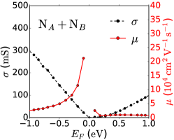
In the top plot of Fig. 12 we show the low-temperature transport characteristics of disordered -doped WSe2 with a concentration of Se vacancies corresponding to the defect density ( cm-2) in recently fabricated high-quality flux-grown TMDs Edelberg et al. (2019); Rhodes et al. (2019). The conductivity is obtained from Eq. (42) using our DFT-calculated hole mass (), and with the relaxation time calculated from Eq. (III.2.3) using DFT inputs for the band structure and matrix.
In -doped WSe2, the carrier density scales with the Fermi level as . The energy range considered in Fig. 12 thus corresponds to typical values of the carrier densities accessible in experiments. The conductivity and mobility in Fig. 12 directly probe the energy dependence of the scattering rate shown in Fig. 11. Since the scattering rate decreases with energy, the conductivity exhibits an initial sublinear density dependence, which translates into a mobility that decreases with carrier density. The characteristic density scaling of the mobility in Fig. 12 is therefore a direct fingerprint of the inherent energy dependence of the -matrix scattering amplitude for point defects in 2D TMDs.
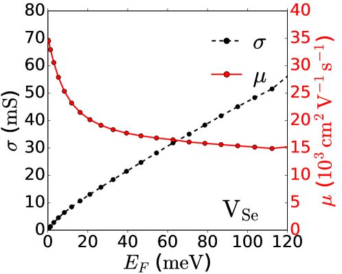
Another important observation to make from Fig. 12 is the overall large magnitude of the carrier mobility, – , which exceeds all previously reported experimental values, so far not exceeding Baugher et al. (2013); Schmidt et al. (2014); Yu et al. (2014); Cui et al. (2015); Schmidt et al. (2016); Fallahazad et al. (2016); Cui et al. (2017); Pisoni et al. (2018a); Gustafsson et al. (2018); Larentis et al. (2018); Pisoni et al. (2018b); Chu et al. (2019). The large theoretical mobility predicted here is a hallmark of (i) the low defect density used in the calculation which corresponds to high-quality TMDs Rhodes et al. (2019), and (ii) the absence of the above-mentioned defect charging which leads to a significant reduction of the mobility due to charged-impurity scattering Kaasbjerg et al. (2019). Both factors are essential for the realization of high-mobility monolayer TMD samples.
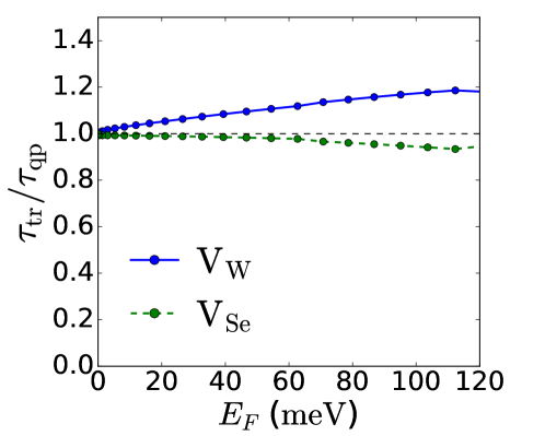
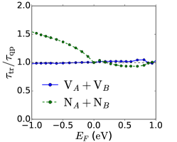
Finally, the bottom plot in Fig. 12 shows the ratio between the transport scattering time and the quantum (quasiparticle) scattering time which is accessible from Shubnikov–de Haas oscillations in magnetotransport Kormányos et al. (2015). The close-to-unity value of the ratio is a direct manifestation of a weak dependence of the -matrix scattering amplitude in the valleys which is inherited from the Se vacancy defect matrix element in Fig. 2. In this case, the term in the transport relaxation time in Eq. (III.2.3) vanishes, and the two scattering times become identical.
Aside from the impact on the longitudinal conductivity considered here, other theoretical works have studied the effect of disorder in 2D TMDs on various other properties such as, e.g., the optical conductivity Yuan et al. (2014), excitons and optical absorption Ekuma and Gunlycke (2018), localization Lu et al. (2013); Ochoa et al. (2014); Ilić et al. (2019), and spin and valley Hall effects Shan et al. (2013); Olsen and Souza (2015). Extensions to studies based on atomistic descriptions of the defect potential offer interesting perspectives for future developments.
V Disordered graphene
Graphene is known to host a wide variety of atomic-scale point defects which are predicted to introduce resonant states on the Dirac cone associated with quasibound defect states Pereira et al. (2006); Wehling et al. (2007); Peres et al. (2006); Ducastelle (2013). The energy of such quasibound states depends on the interaction between the defect and the graphene lattice which is highly sensitive to the position of the defect Duffy et al. (2016); Ruiz-Tijerina and Dias da Silva (2016); Irmer et al. (2018). For vacancies and substitutional atoms, quasibound states with energies in direct vicinity of the Dirac point arise in a robust manner. In transport, such defects act as resonant scatterers exhibiting a strong peak in the scattering cross section at the resonance energy which suppresses the conductivity Ostrovsky et al. (2006); Basko (2008) and affects electron cooling Kong et al. (2018); Tikhonov et al. (2018).
In the following, we focus on monoatomic vacancies and nitrogen (N) substitutionals on the and/or sublattice.
V.1 DOS and spectral function
The DOS of disordered graphene has been studied in numerous works (see, e.g., Refs. Pereira et al., 2006; Peres et al., 2006; Pereira et al., 2008; Hu et al., 2008) addressing, e.g., defect-induced resonant states and band-gap openings. Below we separate the discussion in two cases: (1) sublattice-asymmetric disorder, i.e. defects located exclusively on one sublattice, and (2) sublattice-symmetric disorder where the defects are distributed equally between the and sublattices.
V.1.1 Sublattice asymmetric disorder
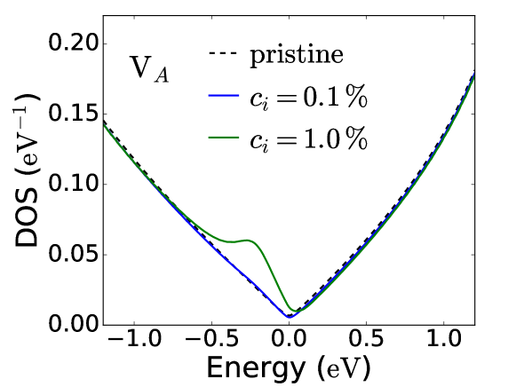
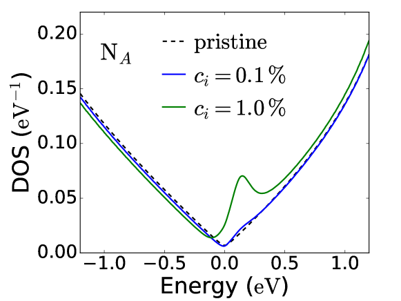
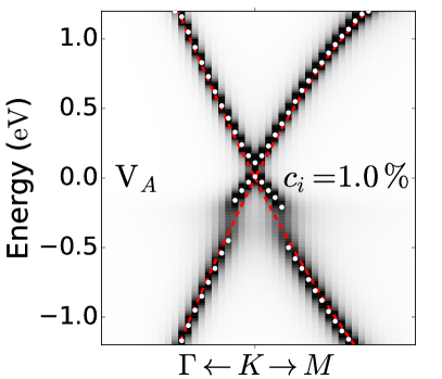
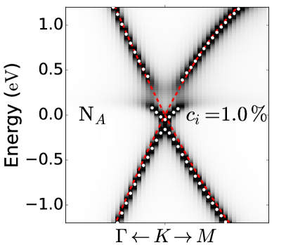
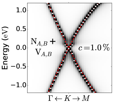
In Fig. 13, we show the DOS for disordered graphene with vacancies (top) and N substitutionals (bottom) located on only the sublattice (VA and NA). At low concentration, , the DOS is hardly discernible from the DOS of pristine graphene. By contrast, at a clear peak in the DOS associated with a quasibound resonant state emerges, respectively, below and above the Dirac point for VA and NA defects. This is in agreement with STM studies of the LDOS Zhao et al. (2011); Joucken et al. (2012); Mao et al. (2016). Our finding for the position of the vacancy bound state contrasts previous theoretical studies based on tight-binding modeling Peres et al. (2006); Wehling et al. (2010); Ferreira et al. (2011); Ducastelle (2013); Irmer et al. (2018); Kot et al. (2018), which predict the resonant state to be at the Dirac point. In our analysis below we comment on this discrepancy.
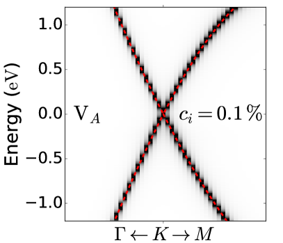
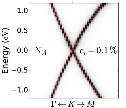
Figure 14 shows plots of the spectral functions corresponding to the different defects and concentrations in Fig. 13. The spectral function at reflects the pristine bands (red dashed lines), although a finite broadening due to disorder scattering, here masked by the numerical broadening , is present (see also Fig. 17 below). For , the Dirac cone is strongly perturbed due to resonant scattering at the position of the quasibound defect states in the DOS. In addition to a pronounced broadening of the states which completely washes out the Dirac cone, this also produces a significant renormalization of the bands below and above the position of the resonance. Signatures of such effects in ARPES on nitrogen-doped graphene have so far not been observed Usachov et al. (2011); Sforzini et al. (2016), probably because the concentration of N substitutionals is too low.
By closer inspection of the spectral functions in Fig. 14, a concentration-dependent band-gap opening can be observed at the Dirac point which at is meV. This is expected as defects located on a single sublattice break the sublattice symmetry, effectively turning the disordered system into gapped graphene Rostami and Cappelluti (2017) as also demonstrated in other theoretical works considering sublattice-asymmetric disorder Pereira et al. (2008); Lherbier et al. (2013); Aktor et al. (2016). Band-gap openings have also been reported experimentally in ARPES on nitrogen-doped graphene Usachov et al. (2011) and graphene with hydrogen adatoms Balog et al. (2010), but the underlying mechanism is believed to be of a different nature, i.e., not associated with sublattice asymmetry.
To shed additional light on the band-gap opening as well as the resonant spectral features, the GF in the subspace spanned by the valence and conduction bands. In this subspace, the diagonal elements obtained by matrix inversion of the Dyson equation (22) take the form
| (44) |
where the effective self-energy is given by
| (45) |
Here, the second term introduced by the matrix inversion describes a defect-induced coupling between the valence and conduction bands, and is responsible for the band-gap opening.
The effective self-energy in Eq. (45) based on the DFT calculated matrix for N substitutionals is shown in the left top plot of Fig. 15 for . Here, the solution to the transcendental equation for the QP equation in Eq. (30) corresponds to the intersection between the solid (green) and dashed lines. Clearly, the effective self-energy shows a feature just below the Dirac point which gives rise to two solutions of the QP equation, corresponding, respectively, to the top of the valence band and the bottom of the conduction band, and hence mark a band-gap opening.
The feature in the effective self-energy responsible for the band-gap opening can be analyzed further based on the TB defect model introduced in Sec. II.3.2. In this case, we can solve Eq. (20) for the matrix analytically, yielding a -independent matrix which in the pseudospin basis inherits the matrix structure of the defect potential in Eq. (15),
| (46) |
where the prefactor is given by
| (47) |
and is the -summed GF for pristine graphene. In the Dirac model, it is given by
| (48) |
where , is the valley degeneracy, and is an ultraviolet cutoff.
Performing a unitary transformation to the eigenstate basis (as the results below are independent on the valley index we omit it here), the -matrix self-energy in Eq. (24) becomes
| (49) |
where the sign on the off-diagonal elements is for defects on the sublattice. In either case, the diagonal elements of the GF again take the form in Eq. (44), with the effective self-energy now given by,
| (50) |
To see the role of the second term for the band-gap opening, we note that in the vicinity of the Dirac point, i.e. , and hence the matrix in Eq. (47) can be approximated as , where . In the effective self-energy in Eq. (50) this leads to a pole in the second term which for the Dirac-point self-energy, i.e. , is located at .

The right top plot in Fig. 15 shows the analytic TB self-energy in Eq. (50) for parameters corresponding to N substitutionals (see caption). The parameters have been obtained by fitting to the DFT self-energy as follows: We first fix to a value resembling the average value of the intravalley and intervalley matrix elements in Fig. 3, and then treat as a fitting parameter in order to match the DFT self-energies in Fig. 15. This is in contrast to the Debye-model inspired approach in Ref. Peres et al., 2006, which is here found to be unable to yield a satisfactory description of the DFT self-energy.
Remarkably, the DFT- and TB-calculated self-energies are in almost perfect agreement. However, due to (i) the nontrivial dependence of the matrix elements in Fig. 3, and (ii) the finite numerical broadening used in the DFT calculation of the -matrix self-energy, some quantitative differences arise.
Via the analytic self-energy in the top plot of Fig. 15, the feature in the DFT self-energy responsible for the band-gap opening can now be identified with the pole introduced by the second term in Eq. (50), which clearly emerges just below the Dirac point, and is seen to give rise to the two solutions to the QP equation also found in the DFT self-energy in Fig. 15. Note that the QP equations for the valence and conduction bands are identical at (since for ), implying that the states at the band-gap opening are formed by a combination of the original valence and conduction band states as in conventional gapped graphene.
In the top plots of Fig. 15, the pole structure in the self-energy at positive energy stems from the pole in the matrix associated with the quasibound defect state in the DOS in Fig. 13. For the matrix in Eq. (47), the pole is positioned at the energy where , and is thus located above (below) the Dirac point for () (see, e.g., Fig. 10 in Ref. Lambin et al., 2012). This is in agreement with our discussion of the parameter for the and defects in Sec. II.3.2. Note that produces a bound state at the Dirac point as discussed in several TB studies of vacancy defects Peres et al. (2006); Wehling et al. (2010); Ducastelle (2013); Irmer et al. (2018); Kot et al. (2018). However, as our DFT calculations here demonstrate, this limiting value of provides an unrealistic description of the vacancy potential and consequently also the position of the quasibound defect state.
In addition to introducing the defect state itself, poles in the matrix also account for resonant scattering off the defect state which strongly perturbs the bands. As evident from the bottom plots in Fig. 14, this introduces a splitting of the conduction band at the resonance energy which resembles a gap opening, but the broadening of the states due to resonant scattering prevents the opening of a spectral gap.
V.1.2 Sublattice symmetric disorder
In Fig. 16 we show the spectral function of disordered graphene () with defects distributed equally on the and sublattices for vacancies (top left), N substitutionals (top right), and both vacancies and N substitutionals (bottom). The two top plots to a large extent resemble the bottom plots for of -only defects in Fig. 14, however, with the important difference that the spectral functions in Fig. 16 do not feature a band-gap opening. In the presence of both and defects, the renormalization of the bands is strongly reduced at energies between the two resonant states in the DOS in Fig. 13 as if the two types of defects cancel the effect of each other.
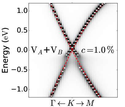
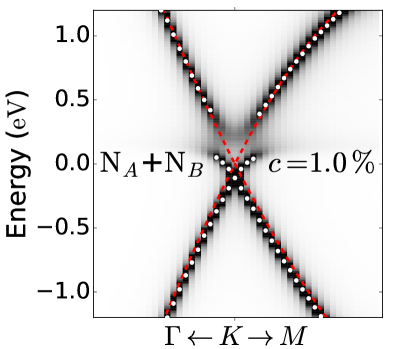
We can again rationalize these findings by considering the GF in the valence and conduction band subspace. As otherwise identical defects on the and the sublattices must be considered as different types of defects, the total self-energy is given by the average over the self-energies for the individual , defects as in Eq. (27), which here amounts to averaging the matrix structure of the self-energies for and sublattice defects Ostrovsky et al. (2006); Basko (2008).
For the DFT self-energy, we find that the sublattice-averaged self-energy is almost perfectly diagonal (not shown), such that the diagonal elements of the GF to a good approximation become
| (51) |
This could also have been anticipated from the TB self-energy where the sublattice average obviously eliminates the off-diagonal elements in Eq. (49) and . Thus, for identical defects distributed equally on the and sublattices, overall sublattice symmetry and, hence the chirality of the graphene states, is conserved.
The two bottom plots in Fig. 15 show, respectively, the DFT and TB self-energies for N substitutionals on both sublattices. Again, there is an excellent qualitative agreement between the TB and DFT self-energies, and quantitative differences can be attributed to the factors mentioned in Sec. V.1.1 above. While the structure in the self-energy due to the pole in the matrix is retained, the form of in the vicinity of the Dirac point does evidently not give rise to a band-gap opening, but only a small downshift of the bands also visible in the right plot of Fig. 16.
In the case of both and defects, the reduction of the band renormalization at energies immediately above and below the Dirac point can be attributed to a partial cancellation between the real parts of the two self-energies in this energy range. This follows straight forwardly from the fact that the self-energy for defects resembles a shifted version of the self-energy for defects in the bottom plot of Fig. 16 with the pole structure centered around the position of the bound-state in Fig. 13.
V.2 Quasiparticle scattering and transport
In this section, we study in further detail the disorder-induced quasiparticle scattering responsible for the spectral linewidth broadening in Figs. 14 and 16 as well as its impact on the transport properties of graphene. In order to avoid complicating the discussion with potential band-gap openings, we here focus on sublattice-symmetric disorder.
In Fig. 17 we show the linewidth broadening in graphene with + nitrogen substituationals () as a function of the on-shell energy on the Dirac cone. The left plot shows a comparison between the Born and -matrix approximations, whereas the right plot shows the individual intravalley and intervalley contributions to the -matrix linewidth in the left plot. Note that the energy dependence of the linewidth has been obtained from points along the -- path in the BZ, and the fact that it forms a single continuous curve along the two line segments shows that it is highly isotropic.
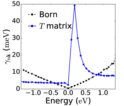
While the energy dependence of the linewidth broadening in the Born approximation reflects the energy dependence of the density of states of pristine graphene in Fig. 13, the -matrix linewidth is strongly electron-hole asymmetric with a pronounced peak on the electron side due to resonant scattering. Also, on the hole side where the DOS of pristine and nitrogen substituted graphene are almost identical (cf. Fig. 13), does the matrix yield a strong renormalization of the Born approximation, with an almost energy independent linewidth broadening.
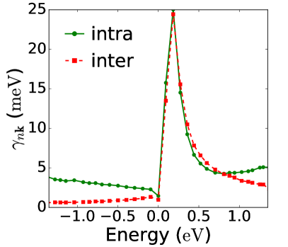
The separation into intravalley and intervalley scattering contributions in the right plot of Fig. 17 reveals that the two types of scattering processes contribute equally to the linewidth broadening at positive energies where resonant scattering dominates. This is in agreement with the TB model in Eqs. (51) and (49). On the contrary, this is not the case on the hole side where intravalley scattering is stronger than intervalley scattering, which can be attributed to the different intravalley and intervalley matrix elements in Fig. 3. Our finding for the strong electron-hole asymmetry in the intervalley scattering rate is in excellent qualitative agreement with recent magnetotransport measurements where the intervalley rate was extracted from the weak localization (WL) correction to the conductivity in nitrogen-doped graphene Li et al. (2017) and graphene with point defect created by ion bombardment Yan et al. (2016).
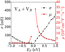
In Fig. 18, the left and center plots show the low-temperature transport characteristics of disordered graphene with a concentration of sublattice symmetric vacancies () and N substitutionals (), respectively. The plots show the conductivity (left axis) and mobility (right axis) as a function of the Fermi level, with the corresponding carrier density scaling as . For both types of defects, the transport exhibits a strong electron-hole asymmetry in the conductivity/mobility which is inherited from the resonant-scattering-induced asymmetry in the underlying scattering rates (cf. Fig. 17). Similar electron-hole asymmetries in the transport characteristics of disordered graphene have been addressed in other theoretical works Basko (2008); Lherbier et al. (2008, 2013), and demonstrated experimentally in defected and nitrogen-doped graphene Chen et al. (2009); Li et al. (2017).
Due to the fact that the quasibound states for the two defects considered in Fig. 18 are, respectively, on the hole and electron sides of the Dirac point (cf. Fig. 13), the two sets of conductivities/mobilities are almost mirror symmetric versions of each other. Considering the large difference in the value of the matrix elements for and defects in Fig. 3, it is perhaps surprising that the magnitude of the conductivities/mobilities are almost identical when comparing the electron (hole) side for with the hole (electron) side for . However, as witnessed by the Born vs -matrix comparison in the left plot of Fig. 17, the bare matrix element which together with the DOS determines the overall magnitude of the Born scattering rate, simply does not reflect the magnitude of the true scattering rate given by the matrix. This holds, in particular, for strong defects where the renormalization of the Born scattering amplitude is most significant.
In the right plot of Fig. 18 we show the ratio between the transport and quantum scattering times as a function of the Fermi energy. In spite of the fact that the transport characteristics for and defects are similar, the ratios between the scattering times for the two types of defects show qualitative differences, in particular, on the hole side. On the basis of the dependence of the matrix elements in Fig. 3, vacancies are expected to behave as short-range disorder (constant matrix element) for which in agreement with Fig. 18. On the other hand, the strong anisotropy and dependence of the matrix element for nitrogen substitutionals reflect a dual short-range and charged-impurity character as also discussed in Sec. II.3.2 above. Since the transport scattering time is less sensitive to small-angle scattering, this results in a ratio larger than unity on the hole side Hwang and Sarma (2008). On the electron side of the Dirac point, the ratio is close to unity as resonant scattering stemming from the short-range nature of the defect potential [cf. the TB model in Eqs. (15) and (47)] dominates.
In order for a complete characterization of the nature of the defects via transport studies, it is thus advantageous to combine measurements of the longitudinal conductivity with measurements of the Shubnikov–de Haas oscillations in the magnetoconductivity from which the quantum scattering time can be inferred.
V.3 Adatoms and adsorbates
In addition to the in-plane defects in graphene considered above, adatoms and molecular adsorbates sitting on top of graphene are also of high relevance as they can be used to functionalize Weeks et al. (2011); Profeta et al. (2012); Santos et al. (2018) and dope Chan et al. (2008) graphene, but may at the same time dominate the transport properties due to resonant scattering off the adatom and adsorbate levels Robinson et al. (2008); Wehling et al. (2009, 2010); Irmer et al. (2018).
In a recent work on disordered Li-decorated graphene Kaasbjerg and Jauho (2019), we demonstrated that in -matrix descriptions of adatoms (we expect that the same holds for other types of adatoms and adsorbates), it is essential to express the matrix and the Dyson equation in Eqs. (19) and (22) in a “complete” Bloch-state basis; i.e., the basis must include bands which describe the electronic structure of both graphene and the surface region where the adatoms are located.
From the point of view of first-principles calculations, the importance of using a complete basis is not a surprising observation. On the other hand, -matrix studies of graphene with adatoms or adsorbates have consistently been based on simple TB models considering a single impurity level coupled to the bands of graphene Robinson et al. (2008); Wehling et al. (2010); Irmer et al. (2018). While this can be expected to capture, e.g., resonant scattering at a qualitative level, it does not account for the fact that the impurity level itself may depend on the impurity concentration via their coupling to socalled surface states Kaasbjerg and Jauho (2019). The two, i.e. resonant scattering and the position of the impurity level, are obviously interconnected and must hence be treated in a self-contained framework.
In the -matrix approach outlined here in Secs. II and III, electronic levels of adatoms and adsorbates enter through the second term in the defect potential in Eq. (12) and emerge as poles in the matrix. In this respect, the method presented here must be expected to give a more complete description of the spectral properties and defect scattering in disordered 2D materials with adatoms and adsorbates Kaasbjerg and Jauho (2019).
VI Discussion and outlook
The first-principles -matrix methodology for modeling the electronic properties of disordered materials presented here, is a natural step beyond first-principles methods based on the Born approximation, see, e.g., Refs. Evans et al., 2005; Lordi et al., 2010; Fedorov et al., 2013; Restrepo et al., 2014; Lu et al., 2019a. As witnessed by the examples included here, this is a critical step in 2D materials where the Born approximation often breaks down and fails to capture even the qualitative picture.
Our work has identified some of the main technical challenges associated with first-principles -matrix calculations as described in Sec. III.3. For example, the large matrix dimensions and memory requirements encountered in the solution of the matrix equation in Eq. (43) call for careful parallelization considerations, beyond the simple multithreading/shared memory approach adopted here. Alternatively, the -matrix equation can be solved in real-space as described in Appendix B by using the supercell LCAO basis in Eq. (4) and with a subsequent transformation to the Bloch-state basis as in Eq. (II.1). This has the immediate advantage that the dimensions of the matrices in Eq. (43) will be fixed to the number of LCAO basis functions in the supercell, which is rather low (– for the supercell sizes considered here). However, this comes at the cost of having to perform the transformation in Eq. (II.1) to the desired -point grid for each energy in the matrix, but this is manageable and can be more efficient when only the -diagonal elements of the matrix (self-energy) are needed.
Irrespective of the strategy chosen for the solution of the -matrix equation, it is essential to use nonuniform -point samplings of the BZ in order to achieve a satisfactory energy resolution in subsequent calculations of, e.g., spectral properties, scattering rates, or transport properties; see, e.g., Refs. Sohier et al., 2018; Poncé et al., 2018; Lu et al., 2019a; Smidstrup et al., 2019 for other recent developments in this direction. As this allows for energy resolutions of the order of meV, our -matrix method is advantageous in comparison to Kubo based approaches Lherbier et al. (2008, 2013); Yuan et al. (2014); Fan et al. (2019) for the calculation of the low-temperature longitudinal conductivity and its dependence on the Fermi energy (carrier density) in dilute, disordered materials.
In addition to the technical aspects of the implementation and the electronic properties discussed in this work, there are several interesting extensions to be considered in future works. For example, a generalization to spin-dependent defect potentials, , accounting for the local change in the spin-orbit interaction around the defect is straight forward, and would allow to address spin-orbit and spin-flip scattering, and hence defect-mediated spin relaxation Fedorov et al. (2013).
A generalization of our method to the treatment of charged defects due to filling of bound defect states by extrinsic carriers presents another highly relevant extension of this work. This requires a self-consistent framework as well as a proper treatment of the resulting long-range Coulomb contribution to the defect potential like in calculations of long-range electron-phonon interactions Verdi and Giustino (2015); Sohier et al. (2016). Preliminary steps for modeling charged defects have recently been reported Aghajanian et al. (2019).
Finally, extensions to other 2D materials and vdW multilayer structures Geim and Grigorieva (2013) as well as to solutions of the Boltzmann equation based on first-principles inputs for the band structure, band velocities, and -matrix scattering amplitude (cf. Appendix A) will be important for the future characterization of the electronic and transport properties of new 2D materials. Also, our method for calculating the defect matrix elements paves the way for new diagrammatic first-principles treatments of, e.g., excitons and optical properties Ekuma and Gunlycke (2018), as well as transport phenomena such as, e.g., localization Altshuler et al. (1980); Lee and Ramakrishnan (1985) and anomalous Hall Sinitsyn et al. (2007); Ferreira et al. (2014); Milletarì and Ferreira (2016); Offidani and Ferreira (2018); Fan et al. (2019) effects in disordered 2D materials.
VII Conclusions
In conclusion, we have presented a DFT based first-principles method for the calculation of defect matrix elements for realistic descriptions of impurities, defects, substitutionals, adatoms, adsorbates, etc., in 2D materials. In combination with a full first-principles based evaluation of the -matrix approximation for the disorder self-energy, we have developed a powerful parameter-free first-principles framework for the description of bound defect states, spectral properties, quasiparticle and carrier scattering, and transport in disordered 2D materials. In spite of the fact that the focus here has been on 2D materials, the method is completely general and can be applied also to 1D and 3D materials. The method is implemented in the GPAW electronic structure code Mortensen et al. (2005); Larsen et al. (2009); Enkovaara et al. (2010).
We first applied the method to defects in the two monolayer TMDs MoS2 and WSe2. We demonstrated that both vacancies and substitutional oxygen give rise to a series of in-gap bound states with some of the states exhibiting a large spin-orbit-induced splitting. As we have discussed in a recent work Kaasbjerg et al. (2019), the presence of in-gap states leads to charging of the defect sites in the extrinsic (i.e., gated) materials, and the resulting charged-impurity scattering has detrimental consequences for the achievable mobility. However, interestingly we find that Se vacancies and oxygen substitutionals in WSe2 only introduce empty in-gap states above the intrinsic Fermi level, implying that these defects will remain charge neutral in extrinsic -type WSe2. In the transport characteristics of high-quality vdW WSe2 devices (– cm-2) free from charged impurities in the substrate Rhodes et al. (2019), this manifests itself in a record-high low-temperature mobility, – , which surprisingly decreases with the carrier density (Fermi energy). The unconventional density dependence of the mobility can be traced back to a strong renormalization of the Born scattering amplitude by multiple-scattering processes accounted for by the matrix. As a consequence, the quantum and transport scattering times become strongly energy dependent and increase away from the band edge. In conjunction with the severe overestimation of the scattering rate by the Born approximation, this underlines the importance of a -matrix treatment of point defects in disordered 2D semiconductors.
We also discussed our previously reported symmetry-induced protection against intervalley scattering by defects in 2D TMDs Kaasbjerg et al. (2017), and showed that it completely suppresses intervalley scattering by, e.g., S vacancies in the conduction band of MoS2, which has often been suggested as the origin of the intervalley scattering extracted from WL/WAL in 2D MoS2 Schmidt et al. (2016); Chu et al. (2019). This finding furthermore points to the possibility of achieving extremely long valley lifetime even in disordered 2D TMDs.
In the last part, we studied the effect of carbon vacancies and nitrogen substitutionals on the electronic properties of graphene. Here, we found that the two types of defects give rise to quasibound resonant states, respectively, below and above the Dirac point. While the latter is in agreement with experimental studies of nitrogen substitutionals in graphene Zhao et al. (2011); Joucken et al. (2012), our finding for the position of the vacancy-induced resonant state below the Dirac point is in contrast to numerous tight-bindings studies where it appears at the Dirac point Peres et al. (2006); Wehling et al. (2010); Ducastelle (2013); Irmer et al. (2018); Kot et al. (2018). For now, we can only speculate that this is due to an oversimplified treatment of the vacancy defect potential in the tight-binding models.
Studying the spectral properties of disordered graphene with, respectively, sublattice-asymmetric and sublattice-symmetric distributions of vacancies and nitrogen substitutionals, we demonstrated defect concentrations of the order of ( cm-2) are required in order to see fingerprints of the resonant states in the spectral function measured in ARPES. We furthermore showed that sublattice-asymmetric disorder with the defects located exclusively on one of the sublattices, opens a concentration-dependent band gap in graphene, which for the above-mentioned concentration is of the order of meV. For sublattice-symmetric disorder, the spectrum again becomes gapless, but retains its characteristic form at the position of the quasibound states caused by strong resonant scattering. In the presence of equal concentrations of sublattice-symmetric vacancies and nitrogen substitutionals, the band renormalization due to the two types of defects cancel each other, which results in a less dramatic deformation of the Dirac cone in the vicinity of the quasibound states.
Finally, we demonstrated that the transport characteristics of disordered graphene become strongly electron-hole asymmetric in the presence of quasibound resonant states.
Altogether, our first-principles-based -matrix method is an important step toward accurate modeling of realistic defects and their impact on the electronic properties of disordered materials.
Acknowledgements.
The author would like to thank J. H. J. Martiny, J. J. Mortensen, N. Papior, M. Brandbyge, T. Olsen and A.-P. Jauho for stimulating discussions and comments on the manuscript. K.K. acknowledges support from the European Union’s Horizon 2020 research and innovation programme under the Marie Sklodowska-Curie Grant Agreement No. 713683 (COFUNDfellowsDTU). The Center for Nanostructured Graphene (CNG) is sponsored by the Danish National Research Foundation, Project No. DNRF103.Appendix A Numerical solution of the Boltzmann equation
The Boltzmann equation in Eq. (39) can be recast as a matrix equation in the composite band and wave-vector index ,
| (52) |
which is solved for . Here, the matrix elements of the collision matrix and the vector on the right-hand side are given, respectively, by
| (53) | ||||
| (54) |
where is the -matrix transition rate in Eq. (40), is the band velocity, and is a unit vector in the direction of the applied electric field. It should be noted that no approximations have been invoked in the solution of the Boltzmann equation outlined above which applies in the case of elastic scattering.
The matrix form of the Boltzmann equation in Eq. (52) appended with the additional particle-conserving constraint on the distribution function, can be solved with a standard least-squares method based on a singular-value decomposition of the collision matrix.
Appendix B -matrix equation in LCAO basis
As an alternative to the Bloch-state formulation of the -matrix equation in Eq. (19) of the main text, it may for practical reason be advantageous to use the LCAO supercell basis as discussed in Sec. VI.
In the nonorthogonal LCAO basis , the completeness relation takes the form , where is the inverse of the overlap matrix defined by . Considering the matrix elements and inserting completeness relations in the -matrix equation , the latter becomes
| (55) |
where the orbital index has been omitted for brevity and .
Like in Sec. III, this can be recast as a matrix equation in the cell and orbital indices,
| (56) |
with the GF given by
| (57) |
The dimension of the matrices is here given by the number of LCAO orbitals in the supercell.
References
- Mounet et al. (2018) N. Mounet, M. Gibertini, P. Schwaller, D. Campi, A. Merkys, A. Marrazzo, T. Sohier, I. E. Castelli, A. Cepellotti, G. Pizzi, and N. Marzari, “Two-dimensional materials from high-throughput computational exfoliation of experimentally known compounds,” Nature Nano. 13, 246 (2018).
- Haastrup et al. (2018) S. Haastrup, M. Strange, M. Pandey, T. Deilmann, P. S. Schmidt, N. F. Hinsche, M. N. Gjerding, D. Torelli, P. M. Larsen, A. C. Riis-Jensen, J. Gath, K. W. Jacobsen, J. J. Mortensen, T. Olsen, and K. S. Thygesen, “The computational 2D materials database: High-throughput modeling and discovery of atomically thin crystals,” 2D Materials 5, 042002 (2018).
- Olsen et al. (2019) T. Olsen, E. Andersen, T. Okugawa, D. Torelli, T. Deilmann, and K. S. Thygesen, “Discovering two-dimensional topological insulators from high-throughput computations,” Phys. Rev. Mat. 3, 024005 (2019).
- Marrazzo et al. (2019) A. Marrazzo, M. Gibertini, D. Campi, N. Mounet, and N. Marzari, “Relative abundance of topological order in exfoliable two-dimensional insulators,” Nano. Lett. 19, 8431 (2019).
- Rhodes et al. (2019) D. Rhodes, S. H. Chae, R. Ribeiro-Palau, and J. Hone, “Disorder in van der Waals heterostructures of 2D materials,” Nature Mat. 18, 541 (2019).
- Wang et al. (2018) K. Wang, K. De Greve, L. A. Jauregui, A. Sushko, A. High, Y. Zhou, G. Scuri, T. Taniguchi, K. Watanabe, M. D. Lukin, H. Park, and P. Kim, “Electrical control of charged carriers and excitons in atomically thin materials,” Nature Nano. 13, 128 (2018).
- Pisoni et al. (2018a) R. Pisoni, Z. Lei, P. Back, M. Eich, H. Overweg, Y. Lee, K. Watanabe, T. Taniguchi, T. Ihn, and K. Ensslin, “Gate-tunable quantum dot in a high quality single layer MoS2 van der Waals heterostructure,” Appl. Phys. Lett. 112, 123101 (2018a).
- Rutter et al. (2007) G. M. Rutter, J. N. Crain, N. P. Guisinger, T. Li, P. N. First, and J. A. Stroscio, “Scattering and interference in epitaxial graphene,” Science 317, 219 (2007).
- Zhao et al. (2011) L. Zhao, R. He, K. T. Rim, T. Schiros, K. S. Kim, H. Zhou, C. Gutiérrez, S. P. Chockalingam, C. J. Arguello, L. Pálová, D. Nordlund, M. S. Hybertsen, D. R. Reichman, T. F. Heinz, P. Kim, A. Pinczuk, G. W. Flynn, and A. N. Pasupathy, “Visualizing individual nitrogen dopants in monolayer graphene,” Science 333, 999 (2011).
- Banhart et al. (2011) F. Banhart, J. Kotakoski, and A. V. Krasheninnikov, “Structural defects in graphene,” ACS Nano 5, 26 (2011).
- Lu et al. (2014) C.-P. Lu, G. Li, J. Mao, L.-M. Wang, and E. Y. Andrei, “Bandgap, mid-gap states, and gating effects in MoS2,” Nano. Lett. 14, 4628 (2014).
- Zhou et al. (2016) X. Zhou, K. Kang, S. Xie, A. Dadgar, N. R. Monahan, X.-Y. Zhu, J. Park, and A. N. Pasupathy, “Atomic-scale spectroscopy of gated monolayer MoS2,” Nano. Lett. 16, 3148 (2016).
- Edelberg et al. (2019) D. Edelberg, D. Rhodes, A. Kerelsky, B. Kim, J. Wang, A. Zangiabadi, C. Kim, A. Abhinandan, J. Ardelean, M. Scully, D. Scullion, L. Embon, R. Zu, Elton J. G. Santos, L. Balicas, C. Marianetti, K. Barmak, X.-Y. Zhu, J. C. Hone, and A. N. Pasupathy, “Approaching the intrinsic limit in transition metal diselenides via point defect control,” Nano. Lett. 19, 4371 (2019).
- Schuler et al. (2019a) B. Schuler, D. Y. Qiu, S. Refaely-Abramson, C. Kastl, C. T. Chen, S. Barja, R. J. Koch, D. F. Ogletree, S. Aloni, A. M. Schwartzberg, J. B. Neaton, S. G. Louie, and A. Weber-Bargioni, “Large spin-orbit splitting of deep in-gap defect states of engineered sulfur vacancies in monolayer WS2,” Phys. Rev. Lett. 123, 076801 (2019a).
- Barja et al. (2019) S. Barja, S. Refaely-Abramson, B. Schuler, D. Y. Qiu, A. Pulkin, S. Wickenburg, H. Ryu, M. M. Ugeda, C. Kastl, C. Chen, C. Hwang, A. Schwartzberg, S. Aloni, S.-K. Mo, D. F. Ogletree, M. F. Crommie, O. V. Yazyev, S. G. Louie, J. B. Neaton, and A. Weber-Bargioni, “Identifying substitutional oxygen as a prolific point defect in monolayer transition metal dichalcogenides,” Nature Commun. 10, 3382 (2019).
- Schuler et al. (2019b) B. Schuler, J.-H. Lee, C. Kastl, K. A. Cochrane, C. T. Chen, S. Refaely-Abramson, S. Yuan, E. van Veen, R. Roldán, N. J. Borys, R. J. Koch, S. Aloni, A. M. Schwartzberg, D. Frank Ogletree, J. B. Neaton, and A. Weber-Bargioni, “How substitutional point defects in two-dimensional WS2 induce charge localization, spin-orbit splitting, and strain,” ACS Nano 13, 10520 (2019b).
- Brihuega et al. (2008) I. Brihuega, P. Mallet, C. Bena, S. Bose, C. Michaelis, L. Vitali, F. Varchon, L. Magaud, K. Kern, and J.-Y. Veuillen, “Quasiparticle chirality in epitaxial graphene probed at the nanometer scale,” Phys. Rev. Lett. 101, 206802 (2008).
- Mallet et al. (2012) P. Mallet, I. Brihuega, S. Bose, M. M. Ugeda, J. M. Gómez-Rodríguez, K. Kern, and J.-Y. Veuillen, “Role of pseudospin in quasiparticle interferences in epitaxial graphene probed by high-resolution scanning tunneling microscopy,” Phys. Rev. B 86, 045444 (2012).
- Chen et al. (2012) L. Chen, C.-C. Liu, B. Feng, X. He, P. Cheng, Z. Ding, S. Meng, Y. Yao, and K. Wu, “Evidence for Dirac fermions in a honeycomb lattice based on silicon,” Phys. Rev. Lett. 109, 056804 (2012).
- Liu et al. (2015) H. Liu, J. Chen, H. Yu, F. Yang, L. Jiao, G.-B. Liu, W. Ho, C. Gao, J. Jia, W. Yao, and M. Xie, “Observation of intervalley quantum interference in epitaxial monolayer tungsten diselenide,” Nature Commun. 6, 8180 (2015).
- Yankowitz et al. (2015) M. Yankowitz, D. McKenzie, and B. J. LeRoy, “Local spectroscopic characterization of spin and layer polarization in WSe2,” Phys. Rev. Lett. 115, 136803 (2015).
- Kiraly et al. (2017) B. Kiraly, N. Hauptmann, A. N. Rudenko, M. I. Katsnelson, and A. A. Khajetoorians, “Probing single vacancies in black phosphorus at the atomic level,” Nano. Lett. 17, 3607 (2017).
- Dombrowski et al. (2017) D. Dombrowski, W. Jolie, M. Petrović, S. Runte, F. Craes, J. Klinkhammer, M. Kralj, P. Lazić, E. Sela, and C. Busse, “Energy-dependent chirality effects in quasifree-standing graphene,” Phys. Rev. Lett. 118, 116401 (2017).
- Jolie et al. (2018) W. Jolie, J. Lux, M. Pörtner, D. Dombrowski, C. Herbig, T. Knispel, S. Simon, T. Michely, A. Rosch, and C. Busse, “Suppression of quasiparticle scattering signals in bilayer graphene due to layer polarization and destructive interference,” Phys. Rev. Lett. 120, 106801 (2018).
- Rammer (1998) J. Rammer, Quantum Transport Theory (Perseus Books, 1998).
- Bruus and Flensberg (2004) H. Bruus and K. Flensberg, Many-body Quantum Theory in Condensed Matter Physics (Oxford University Press, 2004).
- Kaasbjerg et al. (2017) K. Kaasbjerg, J. H. J. Martiny, T. Low, and A.-P. Jauho, “Symmetry-forbidden intervalley scattering by atomic defects in monolayer transition-metal dichalcogenides,” Phys. Rev. B 96, 241411(R) (2017).
- Pereira et al. (2006) V. M. Pereira, F. Guinea, J. M. B. Lopes dos Santos, N. M. R. Peres, and A. H. Castro Neto, “Disorder induced localized states in graphene,” Phys. Rev. Lett. 96, 036801 (2006).
- Pereira et al. (2008) V. M. Pereira, J. M. B. Lopes dos Santos, and A. H. Castro Neto, “Modeling disorder in graphene,” Phys. Rev. B 77, 115109 (2008).
- Hu et al. (2008) B. Yu-Kuang Hu, E. H. Hwang, and S. Das Sarma, “Density of states of disordered graphene,” Phys. Rev. B 78, 165411 (2008).
- Peres et al. (2006) N. M. R. Peres, F. Guinea, and A. H. Castro Neto, “Electronic properties of disordered two-dimensional carbon,” Phys. Rev. B 73, 125411 (2006).
- Wehling et al. (2010) T. O. Wehling, S. Yuan, A. I. Lichtenstein, A. K. Geim, and M. I. Katsnelson, “Resonant scattering by realistic impurities in graphene,” Phys. Rev. Lett. 105, 056802 (2010).
- Ducastelle (2013) F. Ducastelle, “Electronic structure of vacancy resonant states in graphene: A critical review of the single-vacancy case,” Phys. Rev. B 88, 075413 (2013).
- Irmer et al. (2018) S. Irmer, D. Kochan, J. Lee, and J. Fabian, “Resonant scattering due to adatoms in graphene: Top, bridge, and hollow positions,” Phys. Rev. B 97, 075417 (2018).
- Kot et al. (2018) P. Kot, J. Parnell, S. Habibian, C. Straßer, P. M. Ostrovsky, and C. R. Ast, “Band dispersion of graphene with structural defects,” XXX XXX, XXX (2018), arXiv:1811.00087.
- Zou et al. (2016) Y.-L. Zou, J. Song, C. Bai, and K. Chang, “Impurity scattering and Friedel oscillations in monolayer black phosphorus,” Phys. Rev. B 94, 035431 (2016).
- Evans et al. (2005) M. H. Evans, X.-G. Zhang, J. D. Joannopoulos, and S. T. Pantelides, “First-principles mobility calculations and atomic-scale interface roughness in nanoscale structures,” Phys. Rev. Lett. 95, 106802 (2005).
- Lordi et al. (2010) V. Lordi, P. Erhart, and D. Åberg, “Charge carrier scattering by defects in semiconductors,” Phys. Rev. B 81, 235204 (2010).
- Fedorov et al. (2013) D. V. Fedorov, M. Gradhand, S. Ostanin, I. V. Maznichenko, A. Ernst, J. Fabian, and I. Mertig, “Impact of electron-impurity scattering on the spin relaxation time in graphene: A first-principles study,” Phys. Rev. Lett. 110, 156602 (2013).
- Restrepo et al. (2014) O. D. Restrepo, K. E. Krymowski, J. Goldberger, and W. Windl, “A first principles method to simulate electron mobilities in 2D materials,” New J. Phys. 16, 105009 (2014).
- Lu et al. (2019a) I.-T. Lu, J.-J. Zhou, and M. Bernardi, “Efficient ab initio calculations of electron-defect scattering and defect-limited carrier mobility,” Phys. Rev. Materials 3, 033804 (2019a).
- Zhou and Bernardi (2016) Jin-Jian Zhou and Marco Bernardi, “Ab initio electron mobility and polar phonon scattering in GaAs,” Phys. Rev. B 94, 201201 (2016).
- Gunst et al. (2016) Tue Gunst, T. Markussen, K. Stokbro, and M. Brandbyge, “First-principles method for electron-phonon coupling and electron mobility: Applications to two-dimensional materials,” Phys. Rev. B 93, 035414 (2016).
- Sohier et al. (2018) T. Sohier, D. Campi, N. Marzari, and M. Gibertini, “Mobility of two-dimensional materials from first principles in an accurate and automated framework,” Phys. Rev. Materials 2, 114010 (2018).
- Poncé et al. (2018) S. Poncé, E. R. Margine, and F. Giustino, “Towards predictive many-body calculations of phonon-limited carrier mobilities in semiconductors,” Phys. Rev. B 97, 121201(R) (2018).
- Poncé et al. (2020) S. Poncé, W. Li, S. Reichardt, and F. Giustino, “First-principles calculations of charge carrier mobility and conductivity in bulk semiconductors and two-dimensional materials,” Rep. Prog. Phys. XXX, XXX (2020), accepted.
- Lu et al. (2019b) I.-T. Lu, J. Park, J.-J. Zhou, and M. Bernardi, “Ab initio electron-defect interactions using Wannier functions,” XXX (2019b), arXiv:1910.14516.
- Mortensen et al. (2005) J. J. Mortensen, L. B. Hansen, and K. W. Jacobsen, “Real-space grid implementation of the projector augmented wave method,” Phys. Rev. B 71, 035109 (2005).
- Larsen et al. (2009) A. H. Larsen, M. Vanin, J. J. Mortensen, K. S. Thygesen, and K. W. Jacobsen, “Localized atomic basis set in the projector augmented wave method,” Phys. Rev. B 80, 195112 (2009).
- Enkovaara et al. (2010) J. Enkovaara, C. Rostgaard, J. J. Mortensen, J. Chen, M. Dułak, L. Ferrighi, J. Gavnholt, C. Glinsvad, V. Haikola, and H. A. Hansen et al., “Electronic structure calculations with GPAW: a real-space implementation of the projector augmented-wave method,” J. Phys.: Condens. Matt. 22, 253202 (2010).
- Kaasbjerg et al. (2012a) K. Kaasbjerg, K. S. Thygesen, and K. W. Jacobsen, “Phonon-limited mobility in MoS2 from first principles,” Phys. Rev. B 85, 115317 (2012a).
- Kaasbjerg et al. (2012b) K. Kaasbjerg, K. S. Thygesen, and K. W. Jacobsen, “Unraveling the acoustic electron-phonon interaction in graphene,” Phys. Rev. B 85, 165440 (2012b).
- Kaasbjerg et al. (2013) K. Kaasbjerg, K. S. Thygesen, and A.-P. Jauho, “Acoustic phonon-limited mobility in two-dimensional MoS2: Deformation potential and piezoelectric scattering from first principles,” Phys. Rev. B 87, 235312 (2013).
- Blöchl (1994) P. E. Blöchl, “Projector augmented-wave method,” Phys. Rev. B 50, 17953 (1994).
- Giustino et al. (2007) F. Giustino, M. L. Cohen, and S. G. Louie, “Electron-phonon interaction using wannier functions,” Phys. Rev. B 76, 165108 (2007).
- Zhou et al. (2013) W. Zhou, X. Zou, S. Najmaei, Z. Liu, Y. Shi, J. Kong, J. Lou, P. M. Ajayan, B. I. Yakobson, and J.-C. Idrobo, “Intrinsic structural defects in monolayer molybdenum disulfide,” Nano. Lett. 13, 2615 (2013).
- Lin et al. (2014) Y.-C. Lin, T. Björkman, H.-P. Komsa, P.-Y. Teng, C.-H. Yeh, F.-S. Huang, K.-H. Lin, J. Jadczak, Y.-S. Huang, P.-W. Chiu, A. V. Krasheninnikov, and K. Suenaga, “Three-fold rotational defects in two-dimensional transition metal dichalcogenides,” Nature Commun. 6, 6736 (2014).
- Hong et al. (2015) J. Hong, Z. Hu, M. Probert, K. Li, D. Lv, X. Yang, L. Gu, N. Mao, Q. Feng, L. Xie, J. Zhang, D. Wu, Z. Zhang, C. Jin, W. Ji, X. Zhang, J. Yuan, and Z. Zhang, “Exploring atomic defects in molybdenum disulphide monolayers,” Nature Commun. 6, 6293 (2015).
- Komsa et al. (2012) H.-P. Komsa, J. Kotakoski, S. Kurasch, O. Lehtinen, U. Kaiser, and A. V. Krasheninnikov, “Two-dimensional transition metal dichalcogenides under electron irradiation: Defect production and doping,” Phys. Rev. Lett. 109, 035503 (2012).
- Liu et al. (2013) D. Liu, Y. Guo, L. Fang, and J. Robertson, “Sulfur vacancies in monolayer MoS2 and its electrical contacts,” Appl. Phys. Lett. 103, 183113 (2013).
- Noh et al. (2014) J.-Y. Noh, H. Kim, and Y.-S. Kim, “Stability and electronic structures of native defects in single-layer MoS2,” Phys. Rev. B 89, 205417 (2014).
- Komsa and Krasheninnikov (2015) H.-P. Komsa and A. V. Krasheninnikov, “Native defects in bulk and monolayer MoS2 from first principles,” Phys. Rev. B 91, 125304 (2015).
- Zhang et al. (2017) S. Zhang, C.-G. Wang, M.-Y. Li, D. Huang, L.-J. Li, W. Ji, and S. Wu, “Defect structure of localized excitons in a WSe2 monolayer,” Phys. Rev. Lett. 119, 046101 (2017).
- Jiang et al. (2018) Y. Jiang, Z. Chen, Y. Han, P. Deb, H. Gao, S. Xie, P. Purohit, M. W. Tate, J. Park, S. M. Gruner, V. Elser, and D. A. Muller, “Electron ptychography of 2D materials to deep sub-Ångström resolution,” Nature 559, 343 (2018).
- Guguchia et al. (2018) Z. Guguchia, A. Kerelsky, D. Edelberg, S. Banerjee, F. von Rohr, D. Scullion, M. Augustin, M. Scully, D. A. Rhodes, Z. Shermadini, H. Luetkens, A. Shengelaya, C. Baines, E. Morenzoni, A. Amato, J. C. Hone, R. Khasanov, S. J. L. Billinge, E. Santos, A. N. Pasupathy, and Y. J. Uemura, “Magnetism in semiconducting molybdenum dichalcogenides,” Sci. Adv. 4, eaat3672 (2018).
- Moody et al. (2018) G. Moody, K. Tran, X. Lu, T. Autry, J. M. Fraser, R. P. Mirin, L. Yang, X. Li, and K. L. Silverman, “Microsecond valley lifetime of defect-bound excitons in monolayer WSe2,” Phys. Rev. Lett. 121, 057403 (2018).
- Zheng et al. (2019) Y. J. Zheng, Y. Chen, Y. L. Huang, P. K. Gogoi, M. Y. Li, L.-J. Li, P. E. Trevisanutto, Q. Wang, S. J Pennycook, A. T. S. Wee, and S. Y. Quek, “Point defects and localized excitons in 2D WSe2,” ACS Nano 13, 6050 (2019).
- Aghajanian et al. (2019) M. Aghajanian, B. Schuler, K. A. Cochrane, J.-H. Lee, C. Kastl, J. B. Neaton, A. Weber-Bargioni, A. A. Mostofi, and J. Lischner, “Resonant and bound states of charged defects in two-dimensional semiconductor,” Phys. Rev. XXX XXX, XXX (2019), arXiv:1909.02320.
- Luo et al. (2018) Y. Luo, G. D. Shepard, J. V. Ardelean, D. A. Rhodes, B. Kim, K. Barmak, J. C. Hone, and S. Strauf, “Deterministic coupling of site-controlled quantum emitters in monolayer WSe2 to plasmonic nanocavities,” Nature Nano. 13, 1137 (2018).
- Nguyen et al. (2019) P. V. Nguyen, N. C. Teutsch, N. P. Wilson, J. Kahn, X. Xia, A. J. Graham, V. Kandyba, A. Giampietri, A. Barinov, G. C. Constantinescu, N. Yeung, N. D. M. Hine, X. Xu, D. H. Cobden, and N. R. Wilson, “Visualizing electrostatic gating effects in two-dimensional heterostructures,” Nature 572, 220 (2019).
- Xiao et al. (2012) D. Xiao, G.-B. Liu, W. Feng, X. Xu, and W. Yao, “Coupled spin and valley physics in monolayers of MoS2 and other group-VI dichalcogenides,” Phys. Rev. Lett. 108, 196802 (2012).
- Zhu et al. (2011) Z. Y. Zhu, Y. C. Cheng, and U. Schwingenschlögl, “Giant spin-orbit-induced spin splitting in two-dimensional transition-metal dichalcogenide semiconductors,” Phys. Rev. B 84, 153402 (2011).
- Kośmider et al. (2013) K. Kośmider, J. W. González, and J. Fernández-Rossier, “Large spin splitting in the conduction band of transition metal dichalcogenide monolayers,” Phys. Rev. B 88, 245436 (2013).
- Chen et al. (2009) J.-H. Chen, W. G. Cullen, C. Jang, M. S. Fuhrer, and E. D. Williams, “Defect scattering in graphene,” Phys. Rev. Lett. 102, 236805 (2009).
- Ugeda et al. (2010) M. M. Ugeda, I. Brihuega, F. Guinea, and J. M. Gómez-Rodríguez, “Missing atom as a source of carbon magnetism,” Phys. Rev. Lett. 104, 096804 (2010).
- Chen et al. (2011) J.-H. Chen, L. Li, W. G. Cullen, E. D. Williams, and M. S. Fuhrer, “Tunable Kondo effect in graphene with defects,” Nature Phys. 7, 535 (2011).
- Mao et al. (2016) J. Mao, Y. Jiang, D. Moldovan, G. Li, K. Watanabe, T. Taniguchi, M. R. Masir, F. M. Peeters, and E. Y. Andrei, “Realization of a tunable artificial atom at a supercritically charged vacancy in graphene,” Nature Phys. 12, 545 (2016).
- Usachov et al. (2011) D. Usachov, O. Vilkov, Grüneis A., D. Haberer, A. Fedorov, V. K. Adamchuk, A. B. Preobrajenski, P. Dudin, A. Barinov, M. Oehzelt, C. Laubschat, and D. V. Vyalikh, “Nitrogen-doped graphene: Efficient growth, structure, and electronic properties,” Nano. Lett. 11, 5401 (2011).
- Joucken et al. (2012) F. Joucken, Y. Tison, J. Lagoute, J. Dumont, D. Cabosart, B. Zheng, V. Repain, C. Chacon, Y. Girard, A. R. Botello-Méndez, S. Rousset, R. Sporken, J.-C. Charlier, and L. Henrard, “Localized state and charge transfer in nitrogen-doped graphene,” Phys. Rev. B 85, 161408(R) (2012).
- Wehling et al. (2007) T. O. Wehling, A. V. Balatsky, M. I. Katsnelson, A. I. Lichtenstein, K. Scharnberg, and R. Wiesendanger, “Local electronic signatures of impurity states in graphene,” Phys. Rev. B 75, 125425 (2007).
- Duffy et al. (2016) J. Duffy, J. Lawlor, C. Lewenkopf, and M. S. Ferreira, “Impurity invisibility in graphene: Symmetry guidelines for the design of efficient sensors,” Phys. Rev. B 94, 045417 (2016).
- Ruiz-Tijerina and Dias da Silva (2016) D. A. Ruiz-Tijerina and L. G. G. V. Dias da Silva, “Symmetry-protected coherent transport for diluted vacancies and adatoms in graphene,” Phys. Rev. B 94, 085425 (2016).
- Lherbier et al. (2008) A. Lherbier, X. Blase, Y.-M. Niquet, F. Triozon, and S. Roche, “Charge transport in chemically doped 2D graphene,” Phys. Rev. Lett. 101, 036808 (2008).
- Lambin et al. (2012) Ph. Lambin, H. Amara, F. Ducastelle, and L. Henrard, “Long-range interactions between substitutional nitrogen dopants in graphene: Electronic properties calculations,” Phys. Rev. B 86, 045448 (2012).
- Lherbier et al. (2013) A. Lherbier, A. R. Botello-Méndez, and J.-C. Charlier, “Electronic and transport properties of unbalanced sublattice N-doping in graphene,” Nano. Lett. 13, 1446 (2013).
- Hwang et al. (2007) E. H. Hwang, S. Adam, and S. Das Sarma, “Carrier transport in two-dimensional graphene layers,” Phys. Rev. Lett. 98, 186806 (2007).
- Kaasbjerg et al. (2018) K. Kaasbjerg, J. H. J. Martiny, T. Low, and A.-P. Jauho, “A unified description of quasiparticle interference in two-dimensional materials,” in APS March Meeting Abstracts, APS Meeting Abstracts, Vol. 2018 (2018) p. E37.004, http://meetings.aps.org/link/BAPS.2018.MAR.E37.4.
- Altshuler et al. (1980) B. L. Altshuler, D. Khmel’nitzkii, A. I. Larkin, and P. A. Lee, “Magnetoresistance and Hall effect in a disordered two-dimensional electron gas,” Phys. Rev. B 22, 5142 (1980).
- Lee and Ramakrishnan (1985) P. A. Lee and T. V. Ramakrishnan, “Disordered electronic systems,” Rev. Mod. Phys. 57, 287 (1985).
- Kaasbjerg and Jauho (2019) K. Kaasbjerg and A.-P. Jauho, “Signatures of adatom effects in the quasiparticle spectrum of Li-doped graphene,” Phys. Rev. B 100, 241405(R) (2019).
- Elliott et al. (1974) R. J. Elliott, J. A. Krumhansl, and P. L. Leath, “The theory and properties of randomly disordered crystals and related physical systems,” Rev. Mod. Phys. 46, 465 (1974).
- Fan et al. (2019) Z. Fan, J. H. Garcia, A. W. Cummings, J. E. Barrios-Vargas, M. Panhans, A. Harju, F. Ortmann, and S. Roche, “Linear scaling quantum transport methodologies,” Rev. Mod. Phys. XXX, XXX (2019), arXiv:1811.07387.
- Khademi et al. (2019) A. Khademi, K. Kaasbjerg, P. Dosanjh, A. Stöhr, S. Forti, U. Starke, and J. A. Folk, “Weak localization measurements of electronic scattering rates in Li-doped epitaxial graphene,” Phys. Rev. B 100, 161405(R) (2019).
- Olsen (2016) T. Olsen, “Designing in-plane heterostructures of quantum spin Hall insulators from first principles: 1T’-MoS2 with adsorbates,” Phys. Rev. B 94, 235106 (2016).
- Komsa et al. (2014) H.-P. Komsa, N. Berseneva, A. V. Krasheninnikov, and R. M. Nieminen, “Charged point defects in the flatland: Accurate formation energy calculations in two-dimensional materials,” Phys. Rev. X 4, 031044 (2014).
- Carvalho and Neto (2014) A. Carvalho and A. H. Castro Neto, “Donor and acceptor levels in semiconducting transition-metal dichalcogenides,” Phys. Rev. B 89, 081406(R) (2014).
- Haldar et al. (2015) S. Haldar, H. Vovusha, M. K. Yadav, O. Eriksson, and B. Sanyal, “Systematic study of structural, electronic, and optical properties of atomic-scale defects in the two-dimensional transition metal dichalcogenides MX2 (=Mo, W; =S, Se, Te),” Phys. Rev. B 92, 235408 (2015).
- Krivosheeva et al. (2015) A. V. Krivosheeva, V. L. Shaposhnikov, V. E. Borisenko, J.-L. Lazzari, C. Waileong, J. Gusakova, and B. K. Tay, “Theoretical study of defect impact on two-dimensional MoS2,” J. of Semicond. 36, 6 (2015).
- Pandey et al. (2016) M. Pandey, F. A. Rasmussen, K. Kuhar, T. Olsen, K. W. Jacobsen, and K. S. Thygesen, “Defect-tolerant monolayer transition metal dichalcogenides,” Nano. Lett. 16, 2234 (2016).
- Khan et al. (2017) M. A. Khan, M. Erementchouk, J. Hendrickson, and M. N. Leuenberger, “Electronic and optical properties of vacancy defects in single-layer transition metal dichalcogenides,” Phys. Rev. B 95, 245435 (2017).
- Pizzochero and Yazyev (2017) Michele Pizzochero and Oleg V. Yazyev, “Point defects in the and phases of single-layer MoS2: A comparative first-principles study,” Phys. Rev. B 96, 245402 (2017).
- Refaely-Abramson et al. (2018) S. Refaely-Abramson, D. Y. Qiu, S. G. Louie, and J. B. Neaton, “Defect-induced modification of low-lying excitons and valley selectivity in monolayer transition metal dichalcogenides,” Phys. Rev. Lett. 121, 167402 (2018).
- Kaasbjerg et al. (2019) K. Kaasbjerg, T. Low, and A.-P. Jauho, “Electron and hole transport in disordered monolayer MoS2: Atomic vacancy-induced short-range and Coulomb disorder scattering,” Phys. Rev. B 100, 115409 (2019).
- Li et al. (2016) W.-F. Li, C. Fang, and M. A. van Huis, “Strong spin-orbit splitting and magnetism of point defect states in monolayer WS2,” Phys. Rev. B 94, 195425 (2016).
- Zhang et al. (2015) C. Zhang, Y. Chen, A. Johnson, M.-Y. Li, L.-J. Li, P. C. Mendell, R. M. Feenstra, and C.-K. Shih, “Probing critical point energies of transition metal dichalcogenides: Surprising indirect gap of single layer WSe2,” Nano. Lett. 15, 6494 (2015).
- Molina-Sánchez et al. (2016) A. Molina-Sánchez, M. Palummo, A. Marini, and L. Wirtz, “Temperature-dependent excitonic effects in the optical properties of single-layer MoS2,” Phys. Rev. B 93, 155435 (2016).
- Lu et al. (2013) H.-Z. Lu, W. Yao, D. Xiao, and S.-Q. Shen, “Intervalley scattering and localization behaviors of spin-valley coupled Dirac fermions,” Phys. Rev. Lett. 110, 016806 (2013).
- Ochoa et al. (2014) H. Ochoa, F. Finocchiaro, F. Guinea, and V. I. Fal’ko, “Spin-valley relaxation and quantum transport regimes in two-dimensional transition-metal dichalcogenides,” Phys. Rev. B 90, 235429 (2014).
- Schmidt et al. (2016) H. Schmidt, I. Yudhistira, L. Chu, A. H. Castro Neto, B. Özyilmaz, S. Adam, and G. Eda, “Quantum transport and observation of Dyakonov-Perel spin-orbit scattering in monolayer MoS2,” Phys. Rev. Lett. 116, 046803 (2016).
- Ilić et al. (2019) S. Ilić, J. S. Meyer, and M. Houzet, “Weak localization in transition metal dichalcogenide monolayers and their heterostructures with graphene,” Phys. Rev. B 99, 205407 (2019).
- Chu et al. (2019) L. Chu, I. Yudhistira, H. Schmidt, T. C. Wu, S. Adam, and G. Eda, “Phase coherent transport in bilayer and trilayer MoS2,” Phys. Rev. B 100, 125410 (2019).
- Baugher et al. (2013) B. W. H. Baugher, H. O. H. Churchill, Y. Yang, and P. Jarillo-Herrero, “Intrinsic electronic transport properties of high-quality monolayer and bilayer MoS2,” Nano. Lett. 13, 4212 (2013).
- Schmidt et al. (2014) H. Schmidt, S. Wang, L. Chu, M. Toh, R. Kumar, W. Zhao, A. H. Castro Neto, J. Martin, S. Adam, B. Özyilmaz, and G. Eda, “Transport properties of monolayer MoS2 grown by chemical vapor deposition,” Nano. Lett. 14, 1909 (2014).
- Yu et al. (2014) Z. Yu, Y. Pan, Y. Shen, Z. Wang, Z.-Y. Ong, T. Xu, R. Xin, L. Pan, B. Wang, L. Sun, J. Wang, G. Zhang, Y. W. Zhang, Y. Shi, and X. Wang, “Towards intrinsic charge transport in monolayer molybdenum disulfide by defect and interface engineering,” Nature Commun. 5, 5290 (2014).
- Cui et al. (2015) X. Cui, G.-H. Lee, Y. Duck Kim, G. Arefe, P. Y. Huang, C.-H. Lee, D. A. Chenet, X. Zhang, L. Wang, F. Ye, F. Pizzocchero, B. S. Jessen, K. Watanabe, T. Taniguchi, D. A. Muller, T. Low, P. Kim, and J. Hone, “Multi-terminal transport measurements of MoS2 using a van der Waals heterostructure device platform,” Nature Nano. 10, 534 (2015).
- Fallahazad et al. (2016) B. Fallahazad, H. C. P. Movva, K. Kim, S. Larentis, T. Taniguchi, K. Watanabe, S. K. Banerjee, and E. Tutuc, “Shubnikov-de Haas oscillations of high-mobility holes in monolayer and bilayer WSe2: Landau level degeneracy, effective mass, and negative compressibility,” Phys. Rev. Lett. 116, 086601 (2016).
- Cui et al. (2017) X. Cui, E.-M. Shih, L. A. Jauregui, S. H. Chae, Y. D. Kim, B. Li, D. Seo, K. Pistunova, J. Yin, J.-H. Park, H.-J. Choi, Y. H. Lee, K. Watanabe, T. Taniguchi, P. Kim, C. R. Dean, and J. C. Hone, “Low-temperature ohmic contact to monolayer MoS2 by van der Waals bonded Co/-BN electrodes,” Nano. Lett. 17, 4781 (2017).
- Gustafsson et al. (2018) M. V. Gustafsson, M. Yankowitz, C. Forsythe, D. Rhodes, K. Watanabe, T. Taniguchi, J. Hone, X. Zhu, and C. R. Dean, “Ambipolar Landau levels and strong band-selective carrier interactions in monolayer WSe2,” Nature Mat. 17, 411 (2018).
- Larentis et al. (2018) S. Larentis, H. C. P. Movva, B. Fallahazad, K. Kim, A. Behroozi, T. Taniguchi, K. Watanabe, S. K. Banerjee, and E. Tutuc, “Large effective mass and interaction-enhanced Zeeman splitting of -valley electrons in MoSe2,” Phys. Rev. B 97, 201407(R) (2018).
- Pisoni et al. (2018b) R. Pisoni, A. Kormányos, M. Brooks, Z. Lei, P. Back, M. Eich, H. Overweg, Y. Lee, P. Rickhaus, K. Watanabe, T. Taniguchi, A. Imamoglu, G. Burkard, T. Ihn, and K. Ensslin, “Interactions and magnetotransport through spin-valley coupled Landau levels in monolayer MoS2,” Phys. Rev. Lett. 121, 247701 (2018b).
- Kormányos et al. (2015) A. Kormányos, P. Rakyta, and G. Burkard, “Landau levels and Shubnikov-de Haas oscillations in monolayer transition metal dichalcogenide semiconductors,” New J. Phys. 17, 103006 (2015).
- Yuan et al. (2014) S. Yuan, R. Roldán, M. I. Katsnelson, and F. Guinea, “Effect of point defects on the optical and transport properties of MoS2 and WS2,” Phys. Rev. B 90, 041402(R) (2014).
- Ekuma and Gunlycke (2018) C. E. Ekuma and D. Gunlycke, “Optical absorption in disordered monolayer molybdenum disulfide,” Phys. Rev. B 97, 201414(R) (2018).
- Shan et al. (2013) W.-Y. Shan, H.-Z. Lu, and D. Xiao, “Spin Hall effect in spin-valley coupled monolayers of transition metal dichalcogenides,” Phys. Rev. B 88, 125301 (2013).
- Olsen and Souza (2015) T. Olsen and I. Souza, “Valley Hall effect in disordered monolayer MoS2 from first principles,” Phys. Rev. B 92, 125146 (2015).
- Ostrovsky et al. (2006) P. M. Ostrovsky, I. V. Gornyi, and A. D. Mirlin, “Electron transport in disordered graphene,” Phys. Rev. B 74, 235443 (2006).
- Basko (2008) D. M. Basko, “Resonant low-energy electron scattering on short-range impurities in graphene,” Phys. Rev. B 78, 115432 (2008).
- Kong et al. (2018) J. F. Kong, L. Levitov, D. Halbertal, and E. Zeldov, “Resonant electron-lattice cooling in graphene,” Phys. Rev. B 97, 245416 (2018).
- Tikhonov et al. (2018) K. S. Tikhonov, I. V. Gornyi, V. Yu. Kachorovskii, and A. D. Mirlin, “Resonant supercollisions and electron-phonon heat transfer in graphene,” Phys. Rev. B 97, 085415 (2018).
- Ferreira et al. (2011) A. Ferreira, J. Viana-Gomes, J. Nilsson, E. R. Mucciolo, N. M. R. Peres, and A. H. Castro Neto, “Unified description of the dc conductivity of monolayer and bilayer graphene at finite densities based on resonant scatterers,” Phys. Rev. B 83, 165402 (2011).
- Sforzini et al. (2016) J. Sforzini, P. Hapala, M. Franke, G. van Straaten, A. Stöhr, S. Link, S. Soubatch, P. Jelínek, T.-L. Lee, U. Starke, M. Švec, F. C. Bocquet, and F. S. Tautz, “Structural and electronic properties of nitrogen-doped graphene,” Phys. Rev. Lett. 116, 126805 (2016).
- Rostami and Cappelluti (2017) H. Rostami and E. Cappelluti, “Impurity effects and bandgap closing in massive Dirac systems,” Phys. Rev. B 96, 054205 (2017).
- Aktor et al. (2016) T. Aktor, A.-P. Jauho, and S. R. Power, “Electronic transport in graphene nanoribbons with sublattice-asymmetric doping,” Phys. Rev. B 93, 035446 (2016).
- Balog et al. (2010) R. Balog, B. Jørgensen, L. Nilsson, M. Andersen, E. Rienks, M. Bianchi, M. Fanetti, E. Lægsgaard, A. Baraldi, S. Lizzit, Z. Sljivancanin, F. Besenbacher, B. Hammer, T. G. Pedersen, P. Hofmann, and Liv Hornekær, “Bandgap opening in graphene induced by patterned hydrogen adsorption,” Nature Mat. 9, 315 (2010).
- Li et al. (2017) J. Li, L. Lin, D. Rui, Q. Li, J. Zhang, N. Kang, Y. Zhang, H. Peng, Z. Liu, and H. Q. Xu, “Electron-hole symmetry breaking in charge transport in Nitrogen-doped graphene,” ACS Nano 11, 4641 (2017).
- Yan et al. (2016) B. Yan, Q. Han, Z. Jia, J. Niu, T. Cai, D. Yu, and X. Wu, “Electrical control of intervalley scattering in graphene via the charge state of defects,” Phys. Rev. B 93, 041407(R) (2016).
- Hwang and Sarma (2008) E. H. Hwang and S. Das Sarma, “Single-particle relaxation time versus transport scattering time in a two-dimensional graphene layer,” Phys. Rev. B 77, 195412 (2008).
- Weeks et al. (2011) C. Weeks, J. Hu, J. Alicea, M. Franz, and R. Wu, “Engineering a robust quantum spin Hall state in graphene via adatom deposition,” Phys. Rev. X 1, 021001 (2011).
- Profeta et al. (2012) G. Profeta, M. Calandra, and F. Mauri, “Phonon-mediated superconductivity in graphene by lithium deposition,” Nature Phys. 8, 131 (2012).
- Santos et al. (2018) F. J. Santos, D. A. Bahamon, R. B. Muniz, K. McKenna, E. V. Castro, J. Lischner, and A. Ferreira, “Impact of complex adatom-induced interactions on quantum spin Hall phases,” Phys. Rev. B 98, 081407(R) (2018).
- Chan et al. (2008) K. T. Chan, J. B. Neaton, and M. L. Cohen, “First-principles study of metal adatom adsorption on graphene,” Phys. Rev. B 77, 235430 (2008).
- Robinson et al. (2008) J. P. Robinson, H. Schomerus, L. Oroszlány, and V. I. Fal’ko, “Adsorbate-limited conductivity of graphene,” Phys. Rev. Lett. 101, 196803 (2008).
- Wehling et al. (2009) T. O. Wehling, M. I. Katsnelson, and A. I. Lichtenstein, “Impurities on graphene: Midgap states and migration barriers,” Phys. Rev. B 80, 085428 (2009).
- Smidstrup et al. (2019) S. Smidstrup, T. Markussen, P. Vancraeyveld, J. Wellendorff, J. Schneider, T. Gunst, B. Verstichel, D. Stradi, P. A. Khomyakov, U. G. Vej-Hansen, M.-E. Lee, S. T. Chill, F. Rasmussen, G. Penazzi, F. Corsetti, A. Ojanperä, K. Jensen, M. L. N. Palsgaard, U. Martinez, A. Blom, M. Brandbyge, and K. Stokbro, “QuantumATK: An integrated platform of electronic and atomic-scale modelling tools,” J. Phys.: Condens. Matt. 32, 015901 (2019).
- Verdi and Giustino (2015) C. Verdi and F. Giustino, “Fröhlich electron-phonon vertex from first principles,” Phys. Rev. Lett. 115, 176401 (2015).
- Sohier et al. (2016) T. Sohier, M. Calandra, and F. Mauri, “Two-dimensional Fröhlich interaction in transition-metal dichalcogenide monolayers: Theoretical modeling and first-principles calculations,” Phys. Rev. B 94, 085415 (2016).
- Geim and Grigorieva (2013) A. K. Geim and I. V. Grigorieva, “Van der Waals heterostructures,” Nature 499, 419 (2013).
- Sinitsyn et al. (2007) N. A. Sinitsyn, A. H. MacDonald, T. Jungwirth, V. K. Dugaev, and J. Sinova, “Anomalous Hall effect in a two-dimensional Dirac band: The link between the Kubo-Streda formula and the semiclassical Boltzmann equation approach,” Phys. Rev. B 75, 045315 (2007).
- Ferreira et al. (2014) A. Ferreira, T. G. Rappoport, M. A. Cazalilla, and A. H. Castro Neto, “Extrinsic spin Hall effect induced by resonant skew scattering in graphene,” Phys. Rev. Lett. 112, 066601 (2014).
- Milletarì and Ferreira (2016) M. Milletarì and A. Ferreira, “Quantum diagrammatic theory of the extrinsic spin Hall effect in graphene,” Phys. Rev. B 94, 134202 (2016).
- Offidani and Ferreira (2018) M. Offidani and A. Ferreira, “Anomalous Hall effect in 2D Dirac materials,” Phys. Rev. Lett. 121, 126802 (2018).