Shadow epitaxy for in-situ growth of generic semiconductor/superconductor hybrids
Abstract
Uniform, defect-free crystal interfaces and surfaces are crucial ingredients for realizing high-performance nanoscale devices. A pertinent example is that advances in gate-tunable and topological superconductivity using semiconductor/superconductor electronic devices are currently built on the hard proximity-induced superconducting gap obtained from epitaxial indium arsenide/aluminium heterostructures. Fabrication of devices requires selective etch processes; these exist only for InAs/Al hybrids, precluding the use of other, potentially superior material combinations. We present a crystal growth platform – based on three-dimensional structuring of growth substrates – which enables synthesis of semiconductor nanowire hybrids with in-situ patterned superconductor shells. This platform eliminates the need for etching, thereby enabling full freedom in choice of hybrid constituents. We realise and characterise all the most frequently used architectures in superconducting hybrid devices, finding increased yield and electrostatic stability compared to etched devices, along with evidence of ballistic superconductivity. In addition to aluminium, we present hybrid devices based on tantalum, niobium and vanadium.
This is the submitted version of the manuscript. The accepted, peer reviewed version is available from Advanced Materials: http://doi.org/10.1002/adma.201908411
Keywords: superconductor/semiconductor epitaxy, quantum materials, nanowires
One-dimensional semiconductor (SE) nanowires (NWs) proximity coupled to superconductors (SU) have attracted considerable attention from the condensed matter community since the predictionLutchynPRL10 ; OregPRL10 and observationMourikScience12 ; DasNatPhys12 ; DengScience16 of Majorana zero-modes, which have been proposed as a basis for topologically protected quantum information processors.SarmaPRL05 ; AasenPRX16 To ensure topological protection, methods for growing disorder-free ‘hard-gap’ SE/SU epitaxial hybrids were developed.KrogstrupNatMat15 ; ChangNatNano15 ; KangNL17 These materials use bottom-up crystal growth of InAs NWs with uniform epitaxial aluminium coatings, an approach which has been extended to high mobility two-dimensional systemsKjaergaardNatComm16 ; DrachmannNL17 and selective area grown networks.KrizekPRM18 ; VaitiekenasPRL18sag The success of epitaxial InAs/Al hybrids lies in the ability to selectively remove the Al via top-down processing, and thereby realise important device classes such as normal metal spectroscopic devices,DengScience16 ; ChangNatNano15 ; KjaergaardNatComm16 ; DrachmannNL17 Josephson JunctionsvanWoerkomNatPhys17 ; LarocheNatComm19 ; TosiPRX19 ; HaysPRL18 for gate-controlled transmon qubits,LarsenPRL15 ; LuthiPRL18 and superconducting Majorana islands.AlbrechtNature16 ; ShermanNatNano16 ; ProutskiPRB19 A limitation of this method is that the need for post-process etching inherently limits materials choice. For instance, despite strong incentives to utilise technologically important superconductors such as Nb GuskinNanoscale17 and NbTiN GulNL17 – which exhibit higher transition temperatures, critical magnetic fields and superconducting energy gaps – selectively removing Nb from InAs remains an unsolved problem. Similarly, while InSb is an attractive semiconductor due to its high mobility, -factor and strong spin-orbit coupling,GulNL17 ; ZhangNatComm17 ; GulNatNano18 ; ZhangNature18 there is no reported method for selectively removing even Al from InSb without damage. Thus, most potential improvements in epitaxial SE/SU technology are predicated on developing a materials-independent method for device fabrication. An attractive approach to eliminating etch processes is to employ an in-situ ‘shadow approach’ that masks specific segments along the NW from superconductor growth. Initial progress was demonstrated in Refs. 29; 30 where deterministically positioned NWs were shadowed by adjacent NWs. This approach, however, requires accurate control of relative NW positions and growth directions. Further, the range of the possible device geometries is limited, since the NWs create only narrow gaps in the SU coating.
Here, we demonstrate a flexible platform for growing device-ready hybrids in numerous geometries. We combine pre-growth fabrication of shadow structures directly on NW growth substrates with precise positioning of NW growth sites and full in-situ control of the orientation of superconductor flux. The shadow epitaxy platform enables independent materials choice (SU,SE) and we demonstrate simultaneous growth of the most important hybrid device architectures using aluminium, niobium, tantalum and vanadium.BjergfeltNanotech19 Eliminating post-process chemical etching increased spectroscopic device yield (5 out of 5 for Al and Ta devices), enabled ballistic superconductivity in Nb devices, and enhanced electrostatic stability by an order of magnitude in Majorana island devices. Very high yield and large-range, hysteresis-free device operation are crucial metrics for future advanced circuitry that incorporates a large number of hybrid elements. Finally, we show that the platform is compatible with both half-shell and full-shell hybrid geometries and allows for functional devices to be encapsulated in-situ with passivating dielectrics, thus protecting sensitive elements. While the focus here is on semiconductor/superconductor hybrids, shadow epitaxy is equally applicable for any metal/semiconductor/insulator combination, extending the scope to other applications where pristine surfaces and interfaces are key.delAlamoNat11 ; RielMRS14
The shadow epitaxy platform
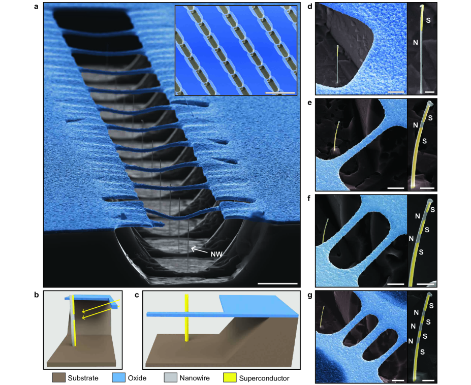
Figure 1 illustrates the platform features. A (111)B-oriented InAs growth substrate is patterned with etched trenches and a series of silicon oxide (SiOx) ‘bridges’. NWs are grown from gold catalyst particles, pre-positioned at the trench bottom with the desired lateral distance from the overhanging bridge(s). NWs are grown by molecular beam epitaxyKrogstrupNatMat15 and the bridges act as shadow masks for subsequent in-situ deposition of superconductors, normal metals, or dielectrics. The material is deposited from a direction parallel to the trenches and inclined by an angle from the substrate surface. The situation is schematically shown in Figure 1b,c. The bridge design is thereby projected as a pattern in the superconducting layer on each NW, effectively growing the desired device architecture, with independent choice of SE and SU material. For process details see Methods and Supplementary Section 1.
To ensure a pristine interface, the sample remains under ultra-high vacuum ( Torr) between NW growth and superconductor deposition.KrogstrupNatMat15 ; BjergfeltNanotech19 ; GuskinNanoscale17 ; KangNL17 ; KjaergaardNatComm16 In the simplest, single-deposition case, the superconductor coats 2 or 3 of the NW’s 6 facets – i.e. a half-shell coating – except for regions shadowed by the bridge. This breaks the NW into a sequence of SU segments separated by bare SE. The length and number of segments are controlled by and the projected bridge design (Supplementary Section 2). Additional possibilities using multiple depositions, angles and/or materials are demonstrated below (Figure 5). Figure 1e-g show scanning electron micrographs (SEMs) of bridges designed to produce the four most important hybrid device geometries. Half-shadowed NWs (Figure 1d) are the canonical design for tunnel-spectroscopy characterisation of the (sub)gap properties of hybrids,ChangNatNano15 ; MourikScience12 ; DengScience16 ; ZhangNature18 and are obtained by shadowing the entire lower section of the NW with a wide bridge. A single, narrow bridge (Figure 1e) produces a gate-tunable Josephson junction,DohScience05 the component at the heart of gatemon and Andreev qubits.LarsenPRL15 ; LuthiPRL18 ; vanWoerkomNatPhys17 ; LarocheNatComm19 ; TosiPRX19 ; HaysPRL18 Double and triple bridges (Figure 1f,g) produce hybrids with singleAlbrechtNature16 ; HigginbothamNatPhys15 ; ShenNatComm18 and doubleShermanNatNano16 Majorana island geometries, respectively, which are the building blocks of topological quantum computation schemes.AasenPRX16 ; PluggeNJP17 In summary, the shadow epitaxy platform enables materials-independent, wafer-scale, parallel synthesis of device-ready hybrids, in many different geometries.
Patterning and structural characterisation of SU films
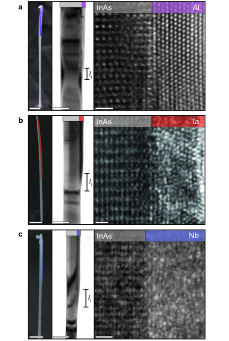
The SU and SE feature sizes are largely defined by the shadow epitaxy mask used, although evaporation chamber geometry and material diffusionKrogstrupNatMat15 become important when high precision is required. In particular, the finite evaporation source size and the distances between NW, mask and source generate ‘tail regions’ between fully covered and fully shadowed segments (Supplementary Section 2). The expected tail length is nm for our mask/chamber dimensions. To characterise this, Figure 2 shows SEM and transmission electron micrographs (TEMs) of InAs hybrids with Al, Ta and Nb shells. Depositions were performed using e-beam evaporation at room temperature except for Al, where C (see Methods), with thicknesses nm, nm, nm (left and middle panel) and nm (right panel). Figure 2 middle panels show typical nm for Nb/Ta and nm for Al. The smaller-than-estimated suggests that material diffusion acts to shorten . The enhanced diffusion and associated shorter for Al is expected from the lower heat of vaporisation; kJ/mol, c.f. kJ/mol.KrogstrupNatMat15 ; BjergfeltNanotech19 Note that these effects can be compensated for by, e.g., altering mask design and NW position, using a smaller deposition source or collimator, and/or double-angle evaporation (Supplementary Section 2).
The semiconductor/superconductor interface properties crucially influence the quality of the induced superconducting gapKrogstrupNatMat15 ; ChangNatNano15 and the rightmost panels in Figure 2 show high resolution TEM of each interface. All interfaces were uniform, with clear semiconductor termination and no interface oxides/contamination. Al and InAs exhibited an epitaxial relation, with the Al growing with out-of-plane orientation. This confirms that shadowed interfaces and e-beam deposited Al retain the high quality and structure of MBE-grown hybrids.KrogstrupNatMat15 ; GuskinNanoscale17 The Ta and Nb films were amorphous/nanocrystalline with a columnar morphology related the deposition angle, as previously observed for Nb GuskinNanoscale17 (Supplementary Section 3). Reliable characterisation of nanocrystalline/amorphous films is challenging due to overlapping signals from randomly oriented grains. However, by imaging a thin ( nm) Ta film, randomly oriented grains with diameter nm can be resolved. An amorphous/nanocrystalline structure was found for Nb depositions both with substrate temperature C and at room temperature.
Tunnel spectroscopy devices
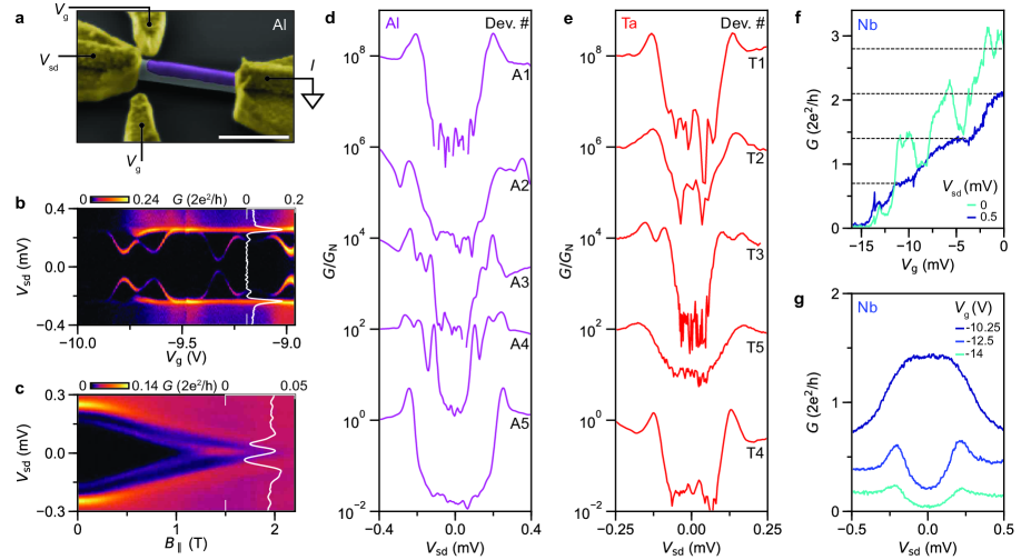
Low temperature transport experiments were performed both to benchmark the shadow-patterned hybrids against the wide literature on etched epitaxial AlKrogstrupNatMat15 ; ChangNatNano15 ; DengScience16 ; AlbrechtNature16 ; HigginbothamNatPhys15 ; ShermanNatNano16 ; ShenNatComm18 ; VaitiekenasPRL18sag ; VaitiekenasPRL18gfactor ; KangNL17 – performance gains are expected due to eliminating post-process etching (Supplementary Section 4) – and to characterise the new Ta and Nb-based hybrids. Figure 3 displays results of tunnel-spectroscopy measurements utilising half-shadowed hybrids (Figure 1d). The exposed SE segment was contacted by a normal metal (Ti/Au) and electrostatic gates were used to induce a quantum dot (QD) or quantum point contact (QPC) tunnel barrier between the Ti/Au and proximitised region.MourikScience12 ; LeeNatNano14 ; ChangNatNano15 ; DengScience16 ; KjaergaardNatComm16 The differential conductance, , in the tunneling regime is proportional to the hybrid density of states, as shown in Figure 3b for Al/InAs. A hard superconducting gap is seen for all with coherence peaks at mV, highlighted by the line trace at V. The gap hardness (where mV) and is the out-of-gap conductance mV)) was throughout the studied range, with a peak value of 350 (Supplementary Section 5). This is the highest reported figure in a SE/SU hybrid, confirming the high quality of the interface. Figure 3c shows the evolution in parallel magnetic field, , with fixed at the position of the line trace of Figure 3b. The gap closes at critical field T; consistent with the thin ( nm), flat, epitaxial film. DengScience16 Coalescing bound states that stick to zero energy for T were also observed – highlighted by the line trace taken with T – resembling previously reported topological zero modes.MourikScience12 ; DengScience16 While a detailed analysis of zero-modes is outside the scope of this article, the magnetic field-compatibility and effective -factor = 6.5VaitiekenasPRL18gfactor highlight the potential of the shadow hybrids for studying the topological regime.
In total, we fabricated five Al/InAs tunnel devices, A1-A5, and logarithmic line traces of normalised conductance vs at fixed are shown in Figure 3d. All five devices exhibited similar behaviour and a hard superconducting gap, with . Devices A2-A4 feature multiple peaks below the coherence peaks at due to bound states (Supplementary Section 6). Overall, the results confirm the high quality of the Al/InAs hybrids synthesised using shadow epitaxy, and the device yield (5 out of 5) compares favourably with conventional device processing using wet etching (Supplementary Section 4).
Turning to devices grown with Ta and Nb, all five Ta/InAs devices exhibited induced superconductivity (Fig 3e). Devices T1-T4 showed hard gaps with values –100, persisting over a wide range (Supplementary Section 6), similar to Al/InAs hybrids. T5 showed a lower hardness . Since the Ta is nanocrystalline/amorphous (Figure 2b) these results show that the atomic ordering of epitaxial interfaces is not a prerequisite for hard gap superconductivity. Rather, an impurity-free, uniform interface is sufficient. The values for meV and corresponding K are consistent with bulk films of matching thickness, 20 nm (Supplementary Section 7).HauserRevModPhys64 The Ta/InAs out-of-plane critical field T (Supplementary Section 7) is significantly higher than for Al/InAs mT with similar dimensions, making Ta/InAs hybrids potentially attractive for studies of topological superconductivity.
The technological importance of niobium based-superconductors – owing to their high K and high critical magnetic fields – has motivated efforts to incorporate them in ex-situ-fabricated hybrid nano-devices.MourikScience12 ; GulNL17 ; ZhangNatComm17 ; GharaviNanotech17 ; DrachmannNL17 Shadow epitaxy enables in-situ Nb/InAs devices previously impossible due to lack of selective process techniques. Figures 3f,g present low-temperature spectroscopic results. Upon increasing , the conductance for mV increases in steps of e2/h and shows a doubling at the plateaus for . This is consistent with a near ballistic junction and near perfect transmission at the contacts.ChuangNL13 ; KjaergaardNatComm16 ; ZhangNatComm17 ; GulNatNano18 In the tunnelling regime, V, conductance suppression is clearly observed for meV in Figure 3g, albeit with relatively low hardness (). Considering the near ballistic device characteristic and high contact transmission, and given the excellent gap hardness achieved in Al/InAs and Ta/InAs shadow devices, it is unlikely the soft superconducting gap for our in-situ Nb/InAs hybrid was caused by contaminated or process-damaged interfaces. Rather, native oxides at the Nb surface could provide an explanation. Nb oxides can be superconducting with lower K, metallic, or magnetic ProslierAPL08 ; HalbritterAPA87 ; each of these effects leads to soft-gap superconductivity in thin niobium films. Using in-situ surface passivation of Nb hybrids would likely provide insights into how the surface impacts gap properties (see Figure 5a). To summarise, the main result of Figure 3 is the demonstration of high-quality hybrid devices with expanded choice of SU and SE.
Stability of in-situ Majorana island devices
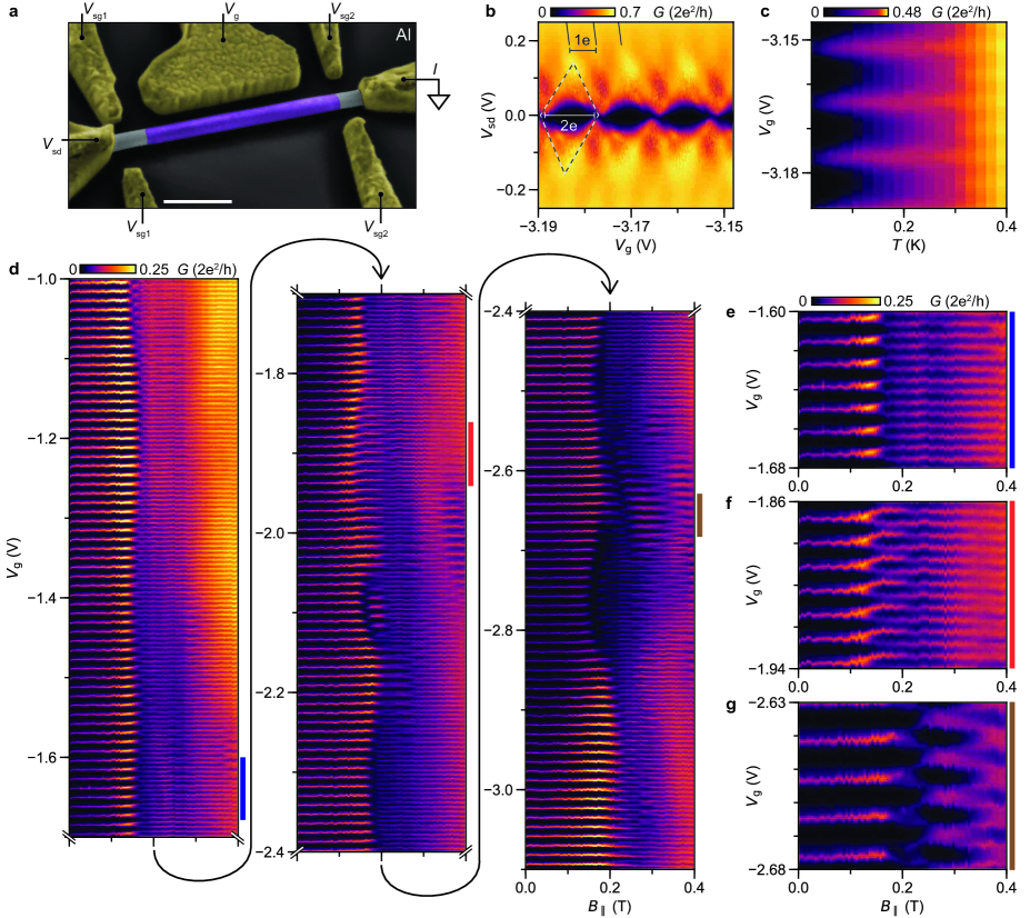
While tunnel spectroscopy devices are the essential tool for characterising induced superconductivity, the elemental building block in most topological quantum computing architectures are ‘Majorana islands’,AasenPRX16 ; PluggeNJP17 which consist of a finite length hybrid segment retaining a charging energy . SingleAlbrechtNature16 and doubleShermanNatNano16 island geometries with arbitrary superconductors are realised using a shadow epitaxy pattern of two or three bridges as shown in Figure 1f,g. The bridge separation(s) and widths determine the lengths of the hybrid segment(s) ) and the exposed NW segments, respectively. Figure 4a shows a typical Al-based shadow-patterned device, measured to enable comparison with conventional etched devices. The gate potentials and control the charge on the island and the tunnel coupling to the Ti/Au leads. AlbrechtNature16 ; HigginbothamNatPhys15 ; ShenNatComm18 ; ProutskiPRB19 For and in the absence of quasi-particles or sub-gap states, charge is added in units of 2 (Cooper pairs). Figure 4b, shows vs. and exhibits -periodic Coulomb diamonds that correspond to a charging energy eV (dashed lines). Quasi-particle 1 periodic charging is seen for eV (solid lines).AlbrechtNature16 ; HigginbothamNatPhys15 Figure 4c shows the temperature dependence of the low-bias -induced charging. The periodic state persists up to mK, where a transition to periodicity occurs due to thermal excitation of quasi-particles. This temperature is set by and the volume of the superconductor and is comparable to that observed in etched devices.HigginbothamNatPhys15 ; VaitiekenasPRL18sag ; ProutskiPRB19
A reproducible and quiet electrostatic platform is crucial for charge-based topological devices, since environmental charge fluctuations and noise couple both to the island charge and tunnel couplings through the semiconductor, and thereby constitute a direct source of qubit decoherence.Knapp:2018 ; Li:2018 Furthermore, with increasing complexity of topological Majorana circuits, fine-tuning in a multi-dimensional space of cross-coupled parameters is required, and stability and reproducibility become important requirements. In conventional etched devices, the stable operation range is typically limited to consecutive charge states,AlbrechtNature16 ; HigginbothamNatPhys15 ; ShenNatComm18 ; VaitiekenasPRL18sag ; ProutskiPRB19 as uncontrolled discrete charging of nearby impurity sites leads to random switches of the island charge/parity. The shadow device exhibits an increase of this range by at least an order of magnitude, consistent with a cleaner electrostatic environment due to the obviation of processing. This is demonstrated in Figure 4d, which shows the stable evolution of 182(364) consecutive 2(1) charge states accessed by continuously sweeping , and an interleaved, step-wise increase of . The island is superconducting in this field range, and the bifurcation of the spectrum at is caused by the appearance of a bound state below the gap, as previously analysed.AlbrechtNature16 ; VaitiekenasPRL18sag ; ShenNatComm18 In addition to a topological transition, various trivial effects can lead to a -transition in , each exhibiting distinct peak spacing and amplitude modulation.AlbrechtNature16 ; VaitiekenasPRL18sag ; ShenNatComm18 For example, the zooms of three regions of panel Figure 4d, shown in Figures 4e-g, exhibit strikingly different behaviors. Figure 4e features -spacings independent of , in Figure 4f the peaks spacing and amplitude are modulated by ,HansenPRB18 while a - transition occurs with a parity change in the range of Figure 4h.ShenNatComm18 The behaviour shown in Figure 4f is consistent with a topological transition;AlbrechtNature16 ; ShenNatComm18 ; Vaitiekenasfullshell18 ; VaitiekenasPRL18sag ; HansenPRB18 ; ShermanNatNano16 however, a detailed study is outside the scope of this work and will be presented elsewhere. The important point here is that the shadow platform greatly enhances the range of hysteresis-free, stable device operation, which in turn facilitates the simultaneous study of different behaviours. Measuring over this larger, stable range provides new information, including the identification of slowly varying features such as the -dependence of the - transitions, which may be linked to gate-dependent -factor of the bound stateVaitiekenasPRL18gfactor or related to weakly coupled bound-states localised in the leads.LeeNatNano14 The potential for increased understanding of device features and large range stability may thus enable reliable and rapid identification of the topological regime. In addition, stable and non-hysteretic navigation in parameter space is a prerequisite for employing automatic tuning and operation procedures that will be essential for operation of complex quantum devices in the future.LennonNPJQuantInf19
Just as the Majorana island is the basic component for topological architectures, gate-tunable Josephson junctions (JJs) constitute the elementary component of superconducting ‘gatemon’LarsenPRL15 ; LuthiPRL18 and Andreev qubit devices.vanWoerkomNatPhys17 ; LarocheNatComm19 ; TosiPRX19 ; HaysPRL18 Electrostatic stability is also critical here for qubit decoherence and tuning.LuthiPRL18 In-situ JJ devices are grown using single-bridge shadows (Figure 1e), and low-temperature characterisation is presented in Supplementary Section 8, demonstrating quiet operation and gate-tunable critical currents nA, consistent with previous devices.LarsenPRL15 ; vanWoerkomNatPhys17 ; LarocheNatComm19
Advanced architectures
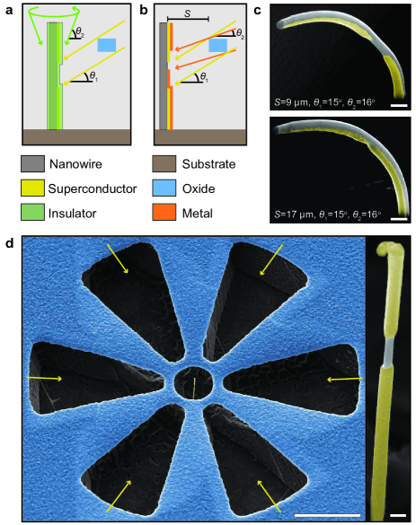
Having demonstrated the use of shadow epitaxy to realise the most important hybrid device geometries, we now discuss further extensions and the flexibility of the method. Firstly, Figure 5a illustrates how steep-angle depositions under rotation enable in-situ conformal dielectric coatings that protect sensitive interfaces, contacts, and surfaces during subsequent device processing. A second extension, illustrated in Figure 5b, employs consecutive shadow depositions from different angles to realise a complete in-situ junction with non-identical contact elements. Such double-angle-generated structures thus produce both lateral and axial hybrid devices incorporating, e.g., normal metal, superconducting and/or magnetic elements with pristine epitaxial interfaces. Double-angle deposition also enables JJ devices with arbitrarily short junction length, as demonstrated in Figure 5c for a vanadium based hybridBjergfeltNanotech19 made by two depositions from different angles , . Conveniently, the semiconductor segment length depends not only the angles and , but also the separation between bridge and NW. Increasing from m to m reduced from nm to nm.
An important feature of our shadow epitaxy platform is the straightforward generalisation to full-shell geometries, achieved by radially copying the bridge design and depositing the coating from corresponding angles around the NW. Figure 5d shows an example full-shell JJ,Vaitiekenasfullshell18 and the other geometries from Figure 1 can be implemented following the same strategy. Deposition of different materials from the various directions further increases the possible functionality. Shadow epitaxy also applies to planar structures such as selective area grown nanostructuresKrizekPRM18 ; VaitiekenasPRL18sag ; SchuffelgenNatNano19 or vapour-liquid-solid NWs grown parallel to the substrateKrizekNL17 (Supplementary Section 9). Finally, we discuss the potential for large scale fabrication using vertical device structures in Supplementary Section 10.
Conclusion
In-situ-grown superconductor/semiconductor hybrid devices form the backbone of electronic implementations of quantum information ranging from topological qubits, gatable transmon devices and Andreev quantum dots. The shadow epitaxy platform transcends previous restrictions on the possible material combinations, and obviates the most potentially damaging fabrication steps, thus providing clear enhancement of device quality and functionality. Beyond these applications, electrical contact quality, reproducibility and surface disorder play an pivotal role in nearly all nanoscale devicesdelAlamoNat11 ; RielMRS14 and thus improving material quality via shadow epitaxy holds the potential to strongly impact also conventional electronics, sensor-applications and optoelectronic devices.delAlamoNat11 ; RielMRS14
Experimental Section
Fabrication of the shadow epitaxy platform. The platform is based on InAs (111)B-oriented substrates, capped with a nm thick SiOx layer grown by plasma-enhanced chemical vapor deposition. The fabrication procedure is illustrated schematically in Supplementary Figure 1. The bridges were formed by two sequential wet etching steps using a single photolithographically defined resist mask (photoresist AZ1505), with the custom pattern exposed using a Heidelberg PG501 LED writer. Etching the SiOx using buffered hydroflouric acid ( in H2O at room temperature) leaves strips of oxide in the desired bridge pattern, with typical length m and widths in the range nm – m. The resist was removed and the InAs was subsequently etched using a 37:23:12 solution of C6H8O7(40%):H3PO4(80%):H2O2 with the SiOx pattern acting as an etch mask. The anisotropic etch preferentially exposes (111)B InAs crystal planes and thereby forms trenches in the substrate, with a (111)B surface at the trench bottom suitable for NW growth. An etch time of 5 mins at room temperature produced trences with depth m. The InAs etchant under-etches material from both sides of each SiOx strip and a void forms underneath the strips since their width . The result is SiOx bridges suspended above the etched InAs surface (Figure 1a). The process is highly reproducible and robust on a wafer scale (Supplementary Figure 2). The potential to use the platform with antimonide, nitride, silicon, and other NW materials is discussed in Supplementary Section 1. Electron beam lithography (PMMA A4.5 and EL13 resist stack) and e-beam deposition of Au were used to define the catalyst particles for NW growth. The platform is naturally compatible with multiple catalyst particles per bridge, and methods for randomly defining catalyst position. Note that fabricating the bridges requires merely a single photolithography step; the complex structures are obtained via relatively simple processing.
Nanowire hybrid growth. InAs NWs were grown via the Au catalyst-assisted vapour-liquid-solid mechanism in a solid-source Varian GEN-II MBE system following a two-step protocol. In the first step, NWs were grown vertically along the (111)B direction, using As4 cracker temperature C, substrate thermocouple temperature of C and V/III flux ratio . A growth time of 80 mins resulted in m-long NWs. The second step involved growth at reduced substrate thermocouple temperature (C) and increased As cracker temperature (C) for 10 mins. These conditions promote radial overgrowth and flatter NW facets, optimal for subsequent superconductor deposition.
After InAs growth, the substrate was transferred under ultra-high vacuum to a metal evaporation chamber, with a freely rotatable sample holder that can be cooled to a thermocouple temperature of approx. C using liquid nitrogen. The low temperature is used to decrease the size and pitch between the initial critical clusters, which promotes a continuous and flat film morphology.KrogstrupNatMat15 It also suppresses the potential for parasitic material to settle outside the shadow-mask defined regions, which may occur in particular for Al depositions at higher temperatures. The superconductor layers (Al, Ta, Nb, V) were deposited using e-beam evaporation at a fixed angle to align with the shadow mask design. The NWs grow with type-I, facets and the shadow mask design is oriented such that the superconductor deposition coats either 2 or 3 of the NW facets, as desired.
Electron microscopy. SEM characterisation of the substrates, as-grown NWs and finished devices was carried out in a JEOL 7800F using acceleration voltage kV. For TEM characterisation, NWs were transferred from the growth substrate to a carbon membrane grid using a micromanipulator under an optical microscope. TEM micrographs were obtained using either a Philips CM20 (Figure 2, center panels) with kV, a FEI Titan Analytical 80-300ST featuring a monochromator and kV (Figure 2a, right panel) or a Phillips 3000F with kV (Figures. 2b,c, right panels). NWs were oriented with the beam parallel to an InAs facet ( zone-axis).
Device fabrication and measurement. NWs were transferred from the growth substrate to pre-patterned device substrates using a micromanipulator under an optical microscope. Ti/Au contacts and side gates were defined simultaneously using electron beam lithography and e-beam deposition. Ar+-ion milling was used immediately prior to contact deposition to remove native InAs oxide and ensure ohmic contact to the NW. Electron transport measurements were conducted in an Oxford Triton dilution refrigerator with a base temperature mK and a 6-1-1 T vector magnet. Standard low frequency ( Hz) lock-in techniques were used to measure differential conductance. For the island device in Figure 4, the cross-coupling of to the tunnel barrier segments was compensated by sweeping simultaneously with using experimentally determined proportionality factors. Note the small offsets in Figures 4d-g between measurements at successive vanish when measuring within a smaller gate range, as in Figures 4b,c. All electrical data throughout this work are presented ‘raw’, without any corrections for switching events.
Acknowledgements.
This work was funded by Innovation Fund Denmark’s Quantum Innovation Center Qubiz, the Carlsberg Foundation, the Danish National Research Foundation, the Villum Foundation, European Union’s Horizon 2020 research and innovation programme FETOpen grant no. 828948 (AndQC) and QuantERA project no. 127900 (SuperTOP). We thank Saulius Vaitiekenas, Asbjørn Drachmann, Juan Carlos Estrada Saldaña, Kasper Grove Rasmussen, Dags Olsteins, Mikelis Marnauza, Lukas Stampfer, Joachim Sestoft, David van Zanten, Peter Krogstrup and I-Ju Chen for many helpful discussions. We also thank Shivendra Upadhyay, Claus B. Sørensen, Ajuan Cui and Thomas Pedersen (DTU Nanolab) for technical assistance and Charline Kirchert and Bilal Kousar for assistance with fabrication.Supporting Information
Supporting Information is available at https://sid.erda.dk/share_redirect/BxJJoUWo0N. Raw electrical data and images for all figures are available from https://doi.org/10.17894/ucph.3a22ad55-37fb-4495-b21d-4294e1e57fcc
References
- (1) R. M. Lutchyn, J. D. Sau, S. Das Sarma, Physical Review Letters 2010, 105, 077001.
- (2) Y. Oreg, G. Refael, F. von Oppen, Physical Review Letters 2010, 105, 177002.
- (3) V. Mourik, K. Zuo, S. M. Frolov, S. R. Plissard, E. P. A. M. Bakkers, L. P. Kouwenhoven, Science 2012, 336, 1003.
- (4) A. Das, Y. Ronen, Y. Most, Y. Oreg, M. Heiblum, H. Shtrikman, Nature Physics 2012, 8, 887.
- (5) M. T. Deng, S. Vaitiekėnas, E. B. Hansen, J. Danon, M. Leijnse, K. Flensberg, J. Nygård, P. Krogstrup, C. M. Marcus, Science 2016, 354, 1557.
- (6) S. Das Sarma, M. Freedman, C. Nayak, Physical Review Letters 2005, 94, 166802.
- (7) D. Aasen, M. Hell, R. V. Mishmash, A. Higginbotham, J. Danon, M. Leijnse, T. S. Jespersen, J. A. Folk, C. M. Marcus, K. Flensberg, J. Alicea, Physical Review X 2016, 6, 031016.
- (8) P. Krogstrup, N. L. B. Ziino, W. Chang, S. M. Albrecht, M. H. Madsen, E. Johnson, J. Nygård, C. M. Marcus, T. S. Jespersen, Nature Materials 2015, 14, 400.
- (9) W. Chang, S. M. Albrecht, T. S. Jespersen, F. Kuemmeth, P. Krogstrup, J. Nygård, C. M. Marcus, Nature Nanotechnology 2015, 10, 232.
- (10) J.-H. Kang, A. Grivnin, E. Bor, J. Reiner, N. Avraham, Y. Ronen, Y. Cohen, P. Kacman, H. Shtrikman, H. Beidenkopf, Nano Letters 2017, 17, 7520.
- (11) M. Kjaergaard, F. Nichele, H. J. Suominen, M. P. Nowak, M. Wimmer, A. R. Akhmerov, J. A. Folk, K. Flensberg, J. Shabani, C. J. Palmstrøm, C. M. Marcus, Nature Communications 2016, 7, 12841.
- (12) A. C. C. Drachmann, H. J. Suominen, M. Kjaergaard, B. Shojaei, C. J. Palmstrøm, C. M. Marcus, F. Nichele, Nano Letters 2017, 17, 1200.
- (13) F. Krizek, J. E. Sestoft, P. Aseev, S. Marti-Sanchez, S. Vaitiekėnas, L. Casparis, S. A. Khan, Y. Liu, T. Stankevič, A. M. Whiticar, A. Fursina, F. Boekhout, R. Koops, E. Uccelli, L. P. Kouwenhoven, C. M. Marcus, J. Arbiol, P. Krogstrup, Physical Review Materials 2018, 2, 093401.
- (14) S. Vaitiekėnas, A. M. Whiticar, M.-T. Deng, F. Krizek, J. E. Sestoft, C. J. Palmstrøm, S. Marti-Sanchez, J. Arbiol, P. Krogstrup, L. Casparis, C. M. Marcus, Physical Review Letters 2018, 121, 147701.
- (15) D. J. van Woerkom, A. Proutski, B. van Heck, D. Bouman, J. I. Väyrynen, L. I. Glazman, P. Krogstrup, J. Nygård, L. P. Kouwenhoven, A. Geresdi, Nature Physics 2017, 13, 876.
- (16) D. Laroche, D. Bouman, D. J. van Woerkom, A. Proutski, C. Murthy, D. I. Pikulin, C. Nayak, R. J. J. van Gulik, J. Nygård, P. Krogstrup, L. P. Kouwenhoven, A. Geresdi, Nature Communications 2019, 10, 1.
- (17) L. Tosi, C. Metzger, M. F. Goffman, C. Urbina, H. Pothier, S. Park, A. L. Yeyati, J. Nygård, P. Krogstrup, Physical Review X 2019, 9, 011010.
- (18) M. Hays, G. de Lange, K. Serniak, D. J. van Woerkom, D. Bouman, P. Krogstrup, J. Nygård, A. Geresdi, M. H. Devoret, Physical Review Letters 2018, 121, 047001.
- (19) T. W. Larsen, K. D. Petersson, F. Kuemmeth, T. S. Jespersen, P. Krogstrup, J. Nygård, C. M. Marcus, Physical Review Letters 2015, 115, 127001.
- (20) F. Luthi, T. Stavenga, O. W. Enzing, A. Bruno, C. Dickel, N. K. Langford, M. A. Rol, T. S. Jespersen, J. Nygård, P. Krogstrup, L. DiCarlo, Physical Review Letters 2018, 120, 100502.
- (21) S. M. Albrecht, A. P. Higginbotham, M. Madsen, F. Kuemmeth, T. S. Jespersen, J. Nygård, P. Krogstrup, C. M. Marcus, Nature 2016, 531, 206.
- (22) D. Sherman, J. S. Yodh, S. M. Albrecht, J. Nygård, P. Krogstrup, C. M. Marcus, Nature Nanotechnology 2017, 12, 212.
- (23) A. Proutski, D. Laroche, B. van ’t Hooft, P. Krogstrup, J. Nygård, L. P. Kouwenhoven, A. Geresdi, Physical Review B 2019, 99, 220504.
- (24) N. A. Güsken, T. Rieger, P. Zellekens, B. Bennemann, E. Neumann, M. I. Lepsa, T. Schäpers, D. Grützmacher, Nanoscale 2017, 9, 16735.
- (25) Ö. Gül, H. Zhang, F. K. de Vries, J. van Veen, K. Zuo, V. Mourik, S. Conesa-Boj, M. P. Nowak, D. J. van Woerkom, M. Quintero-Pérez, M. C. Cassidy, A. Geresdi, S. Koelling, D. Car, S. R. Plissard, E. P. A. M. Bakkers, L. P. Kouwenhoven, Nano Letters 2017, 17, 2690 .
- (26) H. Zhang, Ö. Gül, S. Conesa-Boj, M. P. Nowak, M. Wimmer, K. Zuo, V. Mourik, F. K. de Vries, J. van Veen, M. W. A. de Moor, J. D. S. Bommer, D. J. van Woerkom, D. Car, S. R. Plissard, E. P. A. M. Bakkers, M. Quintero-Pérez, M. C. Cassidy, S. Koelling, S. Goswami, K. Watanabe, T. Taniguchi, L. P. Kouwenhoven, Nature Communications 2017, 8, 16025.
- (27) Ö. Gül, H. Zhang, J. D. S. Bommer, M. W. A. de Moor, D. Car, S. R. Plissard, E. P. A. M. Bakkers, A. Geresdi, K. Watanabe, T. Taniguchi, L. P. Kouwenhoven, Nature Nanotechnology 2018, 13, 192–197.
- (28) H. Zhang, C.-X. Liu, S. Gazibegovic, D. Xu, J. A. Logan, G. Wang, N. van Loo, J. D. S. Bommer, M. W. A. de Moor, D. Car, R. L. M. Op het Veld, P. J. van Veldhoven, S. Koelling, M. A. Verheijen, M. Pendharkar, D. J. Pennachio, B. Shojaei, J. S. Lee, C. J. Palmstrøm, E. P. A. M. Bakkers, S. D. Sarma, L. P. Kouwenhoven, Nature 2018, 556, 74.
- (29) F. Krizek, T. Kanne, D. Razmadze, E. Johnson, J. Nygård, C. M. Marcus, P. Krogstrup, Nano Letters 2017, 17, 6090.
- (30) S. Gazibegovic, D. Car, H. Zhang, S. C. Balk, J. A. Logan, M. W. A. de Moor, M. C. Cassidy, R. Schmits, D. Xu, G. Wang, P. Krogstrup, R. L. M. Op het Veld, K. Zuo, Y. Vos, J. Shen, D. Bouman, B. Shojaei, D. Pennachio, J. S. Lee, P. J. van Veldhoven, S. Koelling, M. A. Verheijen, L. P. Kouwenhoven, C. J. Palmstrøm, E. P. A. M. Bakkers, Nature 2017, 548, 434.
- (31) M. Bjergfelt, D. J. Carrad, T. Kanne, M. Aagesen, E. M. Fiordaliso, E. Johnson, B. Shojaei, C. J. Palmstrøm, P. Krogstrup, T. S. Jespersen, J. N. ard, Nanotechnology 2019, 30, 294005.
- (32) J. A. del Alamo, Nature 2011, 479, 317.
- (33) H. Riel, L.-E. Wernersson, M. Hong, J. A. del Alamo, MRS Bulletin 2014, 39, 668.
- (34) Y.-J. Doh, J. A. van Dam, A. L. Roest, E. P. A. M. Bakkers, L. P. Kouwenhoven, S. D. Franceschi, Science 2005, 309, 272.
- (35) A. P. Higginbotham, S. M. Albrecht, G. Kiršanskas, W. Chang, F. Kuemmeth, P. Krogstrup, T. S. Jespersen, J. Nygård, K. Flensberg, C. M. Marcus, Nature Physics 2015, 11, 1017.
- (36) J. Shen, S. Heedt, F. Borsoi, B. Van Heck, S. Gazibegovic, R. L. M. O. het Veld, D. Car, J. A. Logan, M. Pendharkar, S. J. J. Ramakers, G. Wang, D. Xu, D. Bouman, A. Geresdi, C. J. Palmstrom, E. P. A. M. Bakkers, L. P. Kouwenhoven, Nature Communications 2018, 9, 4801.
- (37) S. Plugge, A. Rasmussen, R. Egger, K. Flensberg, New Journal of Physics 2017, 19, 012001.
- (38) S. Vaitiekėnas, M.-T. Deng, J. Nygård, P. Krogstrup, C. M. Marcus, Physical Review Letters 2018, 121, 037703.
- (39) E. J. H. Lee, X. Jiang, M. Houzet, R. Aguado, C. M. Lieber, S. De Franceschi, Nature Nanotechnology 2014, 9, 79.
- (40) J. J. Hauser, H. C. Theuerer, Reviews of Modern Physics 1964, 36, 80.
- (41) K. Gharavi, G. W. Holloway, R. R. LaPierre, J. Baugh, Nanotechnology 2017, 28, 085202.
- (42) S. Chuang, Q. Gao, R. Kapadia, A. C. Ford, J. Guo, A. Javey, Nano Letters 2013, 13, 555.
- (43) T. Proslier, J. F. Zasadzinski, L. Cooley, C. Antoine, J. Moore, J. Norem, M. Pellin, K. E. Gray, Applied Physics Letters 2008, 92, 212505.
- (44) J. Halbritter, Applied Physics A 1987, 43, 1.
- (45) C. Knapp, T. Karzig, R. M. Lutchyn, C. Nayak, Phys. Rev. B 2018, 97, 125404.
- (46) T. Li, W. A. Coish, M. Hell, K. Flensberg, M. Leijnse, Phys. Rev. B 2018, 98, 205403.
- (47) E. B. Hansen, J. Danon, K. Flensberg, Physical Review B 2018, 97, 041411.
- (48) S. Vaitiekėnas, M.-T. Deng, P. Krogstrup, C. M. Marcus 2018.
- (49) D. T. Lennon, H. Moon, L. C. Camenzind, L. Yu, D. M. Zumbühl, G. a. D. Briggs, M. A. Osborne, E. A. Laird, N. Ares, npj Quantum Information 2019, 5, 1.
- (50) P. Schüffelgen, D. Rosenbach, C. Li, T. W. Schmitt, M. Schleenvoigt, A. R. Jalil, S. Schmitt, J. Kölzer, M. Wang, B. Bennemann, U. Parlak, L. Kibkalo, S. Trellenkamp, T. Grap, D. Meertens, M. Luysberg, G. Mussler, E. Berenschot, N. Tas, A. A. Golubov, A. Brinkman, T. Schäpers, D. Grützmacher, Nature Nanotechnology 2019, 14, 825–831.