Local modified Becke-Johnson exchange-correlation potential for interfaces, surfaces, and two-dimensional materials
Abstract
The modified Becke-Johnson meta-GGA potential of density functional theory has been shown to be the best exchange-correlation potential to determine band gaps of crystalline solids. However, it cannot be consistently used for the electronic structure of non-periodic or nanostructured systems. We propose an extension of this potential that enables its use to study heterogeneous, finite and low-dimensional systems. This is achieved by using a coordinate-dependent expression for the parameter that weights the Becke-Russel exchange, in contrast to the original global formulation, where is just a fitted number. Our potential takes advantage of the excellent description of band gaps provided by the modified Becke-Johnson potential and preserves its modest computational effort. Furthermore, it yields with one single calculation band diagrams and band offsets of heterostructures and surfaces. We exemplify the usefulness and efficiency of our local meta-GGA potential by testing it for a series of interfaces (Si/SiO2, AlAs/GaAs, AlP/GaP, and GaP/Si), a Si surface, and boron nitride monolayer.
European Theoretical Spectroscopy Facility \alsoaffiliationEuropean Theoretical Spectroscopy Facility
1 Introduction
The world around us is inhomogeneous. Approximately homogeneous parts of matter are separated from each other and from the surrounding vacuum by interfaces and surfaces, and these regions are at the origin of a vast number of fascinating and useful phenomena studied across different fields, ranging from biology, over soft matter, to solid-state physics 1. The photoelectric effect, quantum Hall effect, symmetry-protected topological states, or the electron flow in a transistor are well known examples of physics emerging at interfaces or surfaces 2. Understanding electronic properties such as local band gaps, band alignments, energy levels of localized states at interfaces and surfaces is crucial to interpret and control phenomena arising in these regions, opening the way to technological breakthroughs.
The most successful method for the theoretical study of surfaces and interfaces in unquestionably density-functional theory (DFT) 3, 4. This theory combines an unparalleled accuracy with relatively mild computational requirements. In Kohn-Sham DFT all complexities of the many-electron system are included in the so-called exchange-correlation (XC) functional. This is a rather complicated quantity that has to be approximated in any practical use of DFT, and that ultimately determines the quality of the results. Standard semilocal approximations to the XC functionals are quite successful in predicting many properties of solids, such as the atomic structure, phonon spectra or the qualitative band structure. Unfortunately, for an accurate description of band gaps and band alignments, it is necessary to use more advanced approximations, like hybrid functionals 5, 6 or even many-body methods 7, 8. These are computationally much more expensive and can be applied to small surface or interface models only. However, these small models are often not good enough to approximate the inhomogeneous regions of real systems.
A possible way out of this vicious circle is the usage of meta-GGA functionals. Here we will be interested in one meta-GGA functional, the modified Becke-Johnson (MBJ) XC potential 9, which has been optimized for the description of electronic band gaps of homogeneous solids. Various comparisons 10, 11, 12, 13 show that the MBJ is the best semilocal approximation to determine band gaps, achieving on average an accuracy even better than the one of hybrid functionals 13, and at a much lower computational price.
2 Original modified Becke-Johnson potential
The modified Becke-Johnson exchange-correlation potential was proposed by Tran and Blaha in 2009 9. It belongs to the meta-GGA family and its exchange part has the form
| (1) |
where is the electronic density, the kinetic-energy density and
| (2) |
is the Becke-Russel (BR) exchange potential 14, with being calculated from and its spatial gradient and Laplacian and . Together with the LDA correlation, as proposed originally, we will refer to the whole potential as the MBJ XC potential.
The original Becke-Johnson (BJ) potential 15 (obtained with in Eq. 1) was proposed as a sum of the Slater potential 16 describing a Coulomb potential of an exchange hole and , which corrects the error of the Slater potential with respect to the exactly solvable “optimized effective potential” 17 for atoms. Becke and Johnson have further shown that using the BR potential instead of the Slater potential gives almost identical results for atoms 15. In the MBJ potential (Eq. 1) Tran and Blaha used the BR potential, and they introduced a “mixing parameter” reminiscent of the mixing in hybrid functionals. Indeed, the BJ potential models “exact exchange” and the term proportional to can be seen as a screening, thus justifying the analogy to hybrid functionals even further. Led by this analogy and the idea of material dependent mixing 18, Tran and Blaha proposed to determine as
| (3) |
with
| (4) |
averaging in a unit cell. Originally 9, the exponent in Eq. (3) was fixed to and the parameters and were fitted to a set of materials, to minimize the error with respect to their experimental band gaps. Later, an improved fit was performed for resulting in and 19. We chose the latter parameters for this work, as they predict band gaps of semiconductors very close to their experimental values. Other parameters were also obtained recently for more specialized material sets 20, 21.
In spite of its many virtues, analyzed in detail in Ref. 11, the MBJ potential also suffers from drawbacks. For example, it is not a functional derivative of any density functional 22, 23, and therefore it violates a few exact conditions 24 and it cannot be used to calculate total energies. Yet another, more practical, problem originates from the form of Eq. (4). Since is averaged over the whole periodic unit cell, the potential can not be consistently used for inhomogeneous systems. This is better explained with a couple of examples. Let us consider a heterostructure made of two materials with very different values of . In this case, the MBJ potential would use a value of averaged over the whole supercell, leading to an incorrect description of the local band gaps of both constituents. Another example are low-dimensional systems, such as surfaces or molecules. In these cases, converges with the size of the unit cell to a completely inadequate value that depends on the ionization potential of the system. Some groups tried to solve this problem either by fixing the value of to the one of the bulk 25, or by constraining the size of the vacuum region to the value that yields the bulk parameter 26. These procedures might in some cases result in good band gaps in bulk-like regions, but the quality of the description of surfaces is highly questionable.
The impossibility to describe reliably the electronic structure of heterostructures or finite systems is a serious drawback that hampers the systematic application of this meta-GGA potential to evaluate band gaps or band diagrams in high-throughput calculations for computational materials design. For such calculations, the state-of-the-art for band structures remains the more expensive screened hybrid functional HSE06 27, 28, despite its significantly higher computational cost and larger mean average error 13. Here, we propose an effective solution to enable the use of the MBJ potential in automated calculations of nanostructured systems, through an inexpensive local reformulation of the parameter .
3 Formulation of the local MBJ potential
We extend the scheme that we had originally applied to obtain a local hybrid functional for interfaces 29, 30 and we define the locally averaged but spatially varying function
| (5) |
that depends on a smearing parameter . We will discuss in the following how can be determined once and for all, and set as a parameter that defines the potential. The possibility to use a smeared local estimator was suggested by Marques et al. 29 and mentioned as a promising perspective in Refs. 19, 31, but no realization had been attempted yet. The form of in Eq. (5) is particularly convenient because it can be easily implemented into DFT codes using fast-Fourier transforms via a convolution of and the Gaussian in the reciprocal space. We thus introduce the local MBJ (LMBJ) exchange potential with the local parameter given by
| (6) |
with as in Eq. (5) and and .
In principle, the LMBJ potential with the local estimator (Eq. 5) could be already used for surfaces and other systems with vacuum. However, a few problems remain. To recover the correct asymptotic behavior of the XC potential, it is necessary that in the vacuum region. Furthermore, at the matter-vacuum boundary takes values ranging up to 1000 bohr-1, leading to extremely large values of the XC potential and thus hindering the calculation from converging. Another complication arises from the fact that becomes vanishingly small far from the nuclei, leading to numerical instabilities. We solve all these problems by enforcing for regions of low density through the modification
| (7) |
and by introducing a threshold density . For we obtain the previous limit , while in the opposite case and .
Equations 5 and 7 define our LMBJ potential and have been implemented in the VASP code 32. Since the projector-augmented-waves (PAW) method is used 33, the implementation includes a careful treatment of the PAW spheres in addition to the plane-wave part. We give technical details on the implementation in the Supplemental Material.
Before applying the LMBJ potential to realistic systems, we have to choose appropriate values for the parameters and . The length should be as small as possible, to allow for an accurate description of local electronic properties, but also large enough to keep the properties of the original MBJ potential in locally homogeneous regions. We set = 3.78 bohr = 2 Å, which means that is averaged over a region which covers typical interatomic distances. We remark that a similar value was selected for the corresponding parameter in Ref. 30. As shown in Tab. 1 and Fig. 1 of the Supplemental Material, with = 3.78 bohr the calculated band gap reaches its saturation value for all test materials, which in a turn recovers results obtained with the original MBJ potential ( -0.012 , 1.023 bohr1/2, 0.5).
| , | , | , | , | |||
|---|---|---|---|---|---|---|
| material | MBJ | exp | ||||
| Si | 1.11 | 1.20 | 1.20 | 1.18 | 1.27 | 1.17a |
| -SiO2 | 8.85 | 8.63 | 8.59 | 7.88 | 8.13 | 10.30b |
| AlAs | 1.93 | 2.12 | 2.13 | 2.10 | 2.15 | 2.23a |
| GaAs | 1.59 | 1.61 | 1.61 | 1.59 | 1.59 | 1.52a |
| AlP | 2.14 | 2.34 | 2.34 | 2.32 | 2.37 | 2.51a |
| GaP | 2.39 | 2.38 | 2.39 | 2.35 | 2.38 | 2.35a |
| MAE | 0.38 | 0.35 | 0.36 | 0.47 | 0.43 | |
| MAPE | 0.09 | 0.06 | 0.06 | 0.07 | 0.07 |
Concerning the threshold density , we chose a value corresponding to the threshold Wigner-Seitz radius 5 bohr. This value lies well above the value of most of the metals listed in Ref. 35 and our tests show that we obtain bulk band gaps of common semiconductors very close to those yielded by the MBJ potential, see Tab. 1. Clearly, a different choice should be made if one is interested in simulating materials with extremely low electronic densities. Setting 2 bohr increases the deviation from the MBJ band gaps only slightly and leads to an overall underestimation of the band gaps.
Note that further optimization of is not trivial, as it requires a sufficiently large test set with reliable electronic properties for low-dimensional materials. Alternatively, the parameter , possibly together with and , could be fitted to atomic or molecular properties, such as the ionization potential. Of course, the challenge in this case is to recover the predictive power of the MBJ potential for bulk semiconductors.
4 Application of the LMBJ potential
We are going to apply now the LMBJ potential to study band diagrams of electronic systems in which the crystal periodicity is broken in one direction (e.g., ): we therefore consider the local value of averaged in the -plane, , and we calculate the local density of states (LDOS) along the z axis, see the Supplemental Material for details.
An important test of our potential is the Si/SiO2 interface, since the bulk values and the bulk band gaps of the two constituents differ significantly. For this system, we expect that the standard MBJ potential with an averaged value leads to a poor description of the band gaps of both Si and SiO2. To make a direct comparison with calculations in literature possible, we use the same supercell generated by Giustino and Pasquarello 36, already used in Refs. 37, 30. The interface model consists of 11 Si atomic layers along the (001) direction and 10 layers of SiO2 in the -cristobalite form. We adopted an -point grid and a cut-off energy of 400 eV. As in all other calculations in this work, we used PAW pseudopotentials 33 and a spin unpolarized formalism. We first preconverged the calculation using the Perdew-Burke-Ernzerhof (PBE) functional 38 and used the result as a starting point for the subsequent LMBJ calculation.
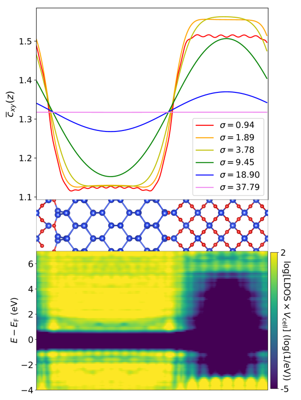
In the top panel of Fig. 1 we show the in-plane averaged local mixing for different values of the smearing . For the very large 37.8 bohr, i.e., a smearing over the whole heterostructure, we obtain as expected a constant mixing . In this limit, our LMBJ potential restores the original MBJ (a reference calculation with the MBJ potential yields ). This calculation thus overestimates, underestimates the -parameter for Si, SiO2 respectively, and consequently the band gaps. Decreasing the smearing leads to a variation of across the slab. We find = 3.78 bohr to be optimal, since it reproduces well the bulk mixing of both Si (heterostructure: , bulk: ) and SiO2 (heterostructure: , bulk: ). Interestingly, our optimal smearing value agrees with the one obtained in Ref. 30 for local hybrids using the same Gaussian smearing of the local mixing parameter applied to the same interface model.
In the bottom panel of Fig. 1 we present the LDOS calculated with the optimal = 3.78 bohr. The local band gaps of Si and SiO2 in the middle of the slab using the LMBJ ( = 1.39 eV, = 8.09 eV) compare well with the MBJ bulk values ( = 1.20 eV, = 8.79 eV, even we can clearly see that the SiO2 layer is too thin to allow for the saturation of the local band gap to the correct bulk value. In fact, we can clearly observe in Fig. 1 that the interface states extend much more inside SiO2 than in Si. In addition to the local band gaps, we can deduce the band offsets at the interface directly from our calculation. We obtain = 1.98 eV and = 4.72 eV for the valence and conduction band offsets, respectively. We should compare these numbers with experimental ( = 4.44 eV and = 3.38 eV 40) and theoretical ( = 4.1 eV and = 2.9 eV 37) and local hybrid values ( = 4.27 eV and = 3.05 eV 30), the latter obtained for the same interface model as in our calculation. The comparison shows that LMBJ gives the correct type of band alignment, with both electrons and holes confined in the SiO2 layer, however the bands of SiO2 are placed 2 eV too high in energy. This is a direct consequence of the fact that, for the Si/SiO2 interface, the LMBJ potential gives basically the same valence band offset as PBE ( = 2.13 eV). Finally, from the local band edges we obtain for the width of the interface 16.6 bohr, which is slightly larger than previous experimental 41 and theoretical 42 results.
We complement the results for the Si/SiO2 interface with band diagrams of other well studied semiconductor interfaces, presented in Tab. 2 in comparison with other theoretical and experimental results.
| A/B heterostructure | (het) | (bulk) | (het) | (bulk) | |||
|---|---|---|---|---|---|---|---|
| PBE | 0.91 | 0.60 | 5.06 | 5.34 | 2.13 | 2.02 | |
| MBJ | 2.02 | 1.27 | 6.92 | 8.13 | 2.13 | 2.77 | |
| Si/SiO2 | LMBJ | 1.39 | 1.20 | 8.09 | 8.71 | 1.98 | 4.72 |
| 1.23 | 4.1a | 2.9a | |||||
| exp | 1.17 | 10.30b | 4.44c | 3.38c | |||
| PBE | 1.13 | 1.41 | 0.74 | 0.70 | 0.35 | 0.04 | |
| MBJ | 2.09 | 2.15 | 1.64 | 1.59 | 0.45 | 0.0 | |
| AlAs/GaAs | LMBJ | 2.03 | 2.13 | 1.80 | 1.59 | 0.63 | -0.40 |
| 2.09 | 1.32 | 0.60 | 0.17 | ||||
| exp | 2.23 | 1.52 | 0.53 | 0.18 | |||
| PBE | 1.49 | 1.56 | 1.53 | 1.61 | 0.28 | -0.31 | |
| MBJ | 2.48 | 2.37 | 2.25 | 2.38 | 0.48 | -0.25 | |
| AlP/GaP | LMBJ | 2.35 | 2.35 | 2.23 | 2.38 | 0.42 | -0.3 |
| 2.50 | 2.59 | 0.67 | -0.76 | ||||
| exp | 2.51 | 2.35 | 0.55 | -0.39 | |||
| PBE | 1.60 | 1.61 | 0.65 | 0.60 | 0.40 | 0.55 | |
| MBJ | 2.27 | 2.38 | 1.40 | 1.27 | 0.31 | 0.56 | |
| GaP/Si | LMBJ | 2.30 | 2.38 | 1.28 | 1.20 | 0.35 | 0.67 |
| 2.59 | 1.23 | 0.53 | 0.83 | ||||
| exp | 2.35 | 1.17 | 0.80 | 0.38 |
For all the systems considered, using LMBJ we obtain local band gaps which agree well with bulk counterparts and experiment (MAPE = 0.11). As expected, PBE systematically underestimates local band gaps (MAPE = 0.41), while MBJ underestimates large band gaps and overestimates small band gaps in very heterogeneous systems (MAPE = 0.19), in particular Si/SiO2.
Concerning the band offsets, we encounter a different behavior of the LMBJ potential for different heterostructures in our limited test set. For Si/SiO2 and GaP/Si . In this case, the error in translates directly to as the experimental band gap is correctly predicted. For the other two systems, AlP/GaP and GaP/Si, we obtain close to the experimental value. For AlP/GaP LMBJ also yields a very good , while for GaP/Si it is slightly worse due to the overestimation of the band gap, leading even to a wrong interface type. A similar behavior for band offsets was obtained with hybrid functionals and calculations 43, as well as with local hybrid functionals 30, although with an overall better performance than LMBJ for the four interfaces. We also find that the results are sensitive to the size of the supercell used to model the interface, as we are extracting band gaps from the value of the local band gap in the middle of the layer. Here we used interface models from the literature to enable comparisons with previous calculations. Those supercells were used originally in two-step calculations, where only the valence band offset was extracted from a supercell calculation, while band gaps were calculated for bulk crystals. We can conclude that one has to pay attention to include more atomic layers to extract accurate band diagrams from a single supercell calculation. In this respect, the use of LMBJ would become particularly advantageous when the supercell is large, due to its reduced computational cost in comparison with hybrid functionals or .
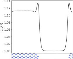
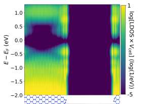
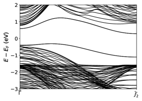
As a next step we consider the application of the LMBJ potential to a crystal with a surface. We chose as a test system the clean (001) surface of silicon with the reconstruction resulting from numerical optimization 44. This model agrees well with both experimental measurements 45 and recent calculations 46. We conducted the LMBJ calculation for a slab consisting of 32 atomic layers and the width of vacuum between periodic slabs was set to 79.4 bohr. The energy cut-off was set to 245.3 eV and we used an -point grid. As for the Si/SiO2 interface, we chose for the smearing 3.78 bohr, and a threshold density corresponding to 5 bohr as justified above.
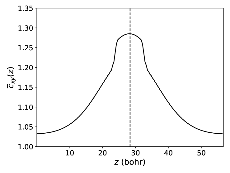
In Fig. 2 (left) we show the converged average along the direction perpendicular to the slab surface. We obtained for in the middle of the slab and for in the vacuum region. The former agrees well with the bulk mixing of Si () and the latter is the desired property of the LMBJ in vacuum. We observe a small peak exactly at the surface, which originates from the large gradient of the density and is thus of a physical origin. Even if varying leads to a different size of this peak, these changes have no significant influence on the local potential, and thus on the electronic structure. This may be different in other materials and should be the subject of further investigations. In Figs. 2 (middle) and (right) we present the LDOS and band structure of the Si slab. For the local band gap in the middle of the slab we obtained 1.26 eV, which agrees well with the bulk calculation. Finally, the two surface states visible in both the LDOS and the band structure match with those calculated in Ref. 46 using hybrid functionals, including their dispersion and distance from the bulk edges.
In our final test we turn to two-dimensional materials. We chose hexagonal boron-nitride (h-BN), since there is a renewed interest in its electronic structure 47, 48 and the band gap of its parent bulk (three-dimensional) structure is described very well by the MBJ potential 19. Bulk h-BN consists of layered honeycomb monolayers with in-plane lattice constant 4.72 bohr and interlayer distance of 6.29 bohr (for the AA’ stacking which was predicted to be most stable 49, 50).
We first calculated the electronic structure of bulk h-BN using the PBE, MBJ and LMBJ (with 7.56 bohr) potentials with an energy cut-off of 400 eV and a -point grid. We obtained band gaps 3.88 eV, 5.64 eV and 5.55 eV. The local mixing of the LMBJ calculation is basically constant in the bulk crystal: . This value is very close to the mixing of a bulk MBJ calculation. Both the MBJ and LMBJ band gaps agree well with the HSE and experimental results of 5.95 eV 50 and 6.08 eV 51, respectively. For the h-BN monolayer we kept the lattice constant 4.72 bohr. The width of vacuum between periodic replicas of the monolayers was set to 56.7 bohr, the energy cut-off was 400 eV and we used a -point grid. The smearing and threshold Wigner-Seitz radius were set to 7.56 bohr and 5 bohr, respectively.
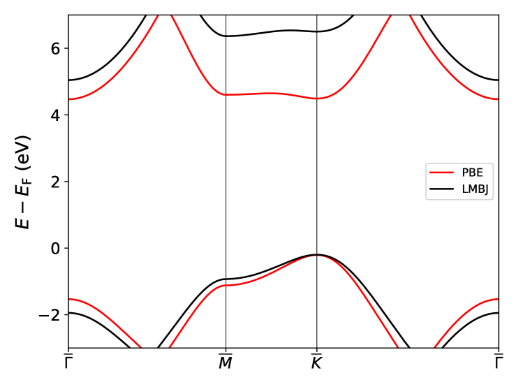
In the top part of Fig. 3 we show the band structure calculated using the PBE and LMBJ potentials. The indirect and direct (at ) band gaps we obtained with PBE were 4.68 eV and 4.70 eV, respectively. This result is improved by the use of the LMBJ potential, which yields 5.25 eV and 6.70 eV. These values improve over PBE and differ by from values obtained by hybrid functional calculations ( 5.68 eV, 6.13 eV 52). Other theoretical and experimental works obtained a direct (indirect) band gap of 6.47 eV 50 and 6.1 eV 53, respectively.
5 Conclusions
We proposed a generalization of the successful MBJ potential introduced by Tran and Blaha 9 to calculate bulk band structures. Our local MBJ potential enables the calculation of band diagrams of heterostructures and the evaluation of energy levels of finite systems. To this end, we defined a position dependent parameter , averaged over a region of approximately one unit cell that replaces the constant parameter of the MBJ potential. We demonstrated that our LMBJ potential allows to obtain band diagrams at interfaces with other materials or with vacuum in a single calculation, reproducing well both surface states and bulk band states inside the layers. We discussed examples of the application of the LMBJ potential to semiconductor interfaces, a Si surface and a h-BN monolayer, demonstrating that it is possible to obtain band gaps of the quality of hybrid functionals even for a 2D material. A large-scale benchmark calculation is currently not possible due to the lack of reliable experimental data for lower-dimensional materials. Thanks to its computational efficiency, the LMBJ potential allows for reliable band structure calculations of large inhomogeneous systems, also when hybrid functional and approaches are computationally too expensive.
This work was supported by the Deutsche Forschungsgemeinschaft (DFG, German Research Foundation) through the projects SFB-762 (project A11), SFB-1375 (project A02), MA 6787/1-1 and BO 4280/8-1. S.B. and T.R. acknowledge funding from the Volkswagen Stiftung (Momentum) through the project “dandelion”.
The Supplemental Material includes details on the implementation of the LMBJ potential into the VASP code, the definition of the LDOS and results of band gap calculations for 3D bulk semiconductors.
References
- Allara 2005 Allara, D. A perspective on surfaces and interfaces. Nature 2005, 437, 638–639
- Brillson 2012 Brillson, L. J. Surfaces and Interfaces of Electronic Materials; John Wiley & Sons, Ltd, 2012
- Hohenberg and Kohn 1964 Hohenberg, P.; Kohn, W. Inhomogeneous Electron Gas. Phys. Rev. 1964, 136, B864–B871
- Kohn and Sham 1965 Kohn, W.; Sham, L. J. Self-Consistent Equations Including Exchange and Correlation Effects. Phys. Rev. 1965, 140, A1133–A1138
- Seidl et al. 1996 Seidl, A.; Görling, A.; Vogl, P.; Majewski, J. A.; Levy, M. Generalized Kohn-Sham schemes and the band-gap problem. Phys. Rev. B 1996, 53, 3764–3774
- Scuseria and Staroverov 2005 Scuseria, G. E.; Staroverov, V. N. In Theory and Applications of Computational Chemistry; Dykstra, C. E., Frenking, G., Kim, K. S., Scuseria, G. E., Eds.; Elsevier: Amsterdam, 2005; pp 669 – 724
- Hedin 1965 Hedin, L. New Method for Calculating the One-Particle Green’s Function with Application to the Electron-Gas Problem. Phys. Rev. 1965, 139, A796–A823
- Onida et al. 2002 Onida, G.; Reining, L.; Rubio, A. Electronic excitations: density-functional versus many-body Green’s-function approaches. Rev. Mod. Phys. 2002, 74, 601–659
- Tran and Blaha 2009 Tran, F.; Blaha, P. Accurate band gaps of semiconductors and insulators with a semilocal exchange-correlation potential. Phys. Rev. Lett. 2009, 102, 226401
- Singh 2010 Singh, D. J. Electronic structure calculations with the Tran-Blaha modified Becke-Johnson density functional. Phys. Rev. B 2010, 82, 205102
- Koller et al. 2011 Koller, D.; Tran, F.; Blaha, P. Merits and limits of the modified Becke-Johnson exchange potential. Phys. Rev. B 2011, 83, 195134
- Tran and Blaha 2017 Tran, F.; Blaha, P. Importance of the Kinetic Energy Density for Band Gap Calculations in Solids with Density Functional Theory. J. Phys. Chem. A 2017, 121, 3318–3325
- Borlido et al. 2019 Borlido, P.; Aull, T.; Huran, A. W.; Tran, F.; Marques, M. A. L.; Botti, S. Large-Scale Benchmark of Exchange–Correlation Functionals for the Determination of Electronic Band Gaps of Solids. J. Chem. Theory Comput. 2019, 15, 5069–5079
- Becke and Roussel 1989 Becke, A. D.; Roussel, M. R. Exchange holes in inhomogeneous systems: A coordinate-space model. Phys. Rev. A 1989, 39, 3761–3767
- Becke and Johnson 2006 Becke, A. D.; Johnson, E. R. A simple effective potential for exchange. J. Chem. Phys. 2006, 124, 221101
- Slater 1951 Slater, J. C. A Simplification of the Hartree-Fock Method. Phys. Rev. 1951, 81, 385–390
- Sharp and Horton 1953 Sharp, R. T.; Horton, G. K. A Variational Approach to the Unipotential Many-Electron Problem. Phys. Rev. 1953, 90, 317–317
- Krukau et al. 2008 Krukau, A. V.; Scuseria, G. E.; Perdew, J. P.; Savin, A. Hybrid functionals with local range separation. J. Chem. Phys. 2008, 129, 124103
- Koller et al. 2012 Koller, D.; Tran, F.; Blaha, P. Improving the modified Becke-Johnson exchange potential. Phys. Rev. B 2012, 85, 155109
- Jishi et al. 2014 Jishi, R. A.; Ta, O. B.; Sharif, A. A. Modeling of Lead Halide Perovskites for Photovoltaic Applications. J. Phys. Chem. C 2014, 118, 28344–28349
- Traoré et al. 2019 Traoré, B.; Bouder, G.; Lafargue-Dit-Hauret, W.; Rocquefelte, X.; Katan, C.; Tran, F.; Kepenekian, M. Efficient and accurate calculation of band gaps of halide perovskites with the Tran-Blaha modified Becke-Johnson potential. Phys. Rev. B 2019, 99, 035139
- Karolewski et al. 2009 Karolewski, A.; Armiento, R.; Kümmel, S. Polarizabilities of Polyacetylene from a Field-Counteracting Semilocal Functional. J. Chem. Theory Comput. 2009, 5, 712–718
- Gaiduk and Staroverov 2009 Gaiduk, A. P.; Staroverov, V. N. How to tell when a model Kohn–Sham potential is not a functional derivative. J. Chem. Phys. 2009, 131, 044107
- Levy and Perdew 1985 Levy, M.; Perdew, J. P. Hellmann-Feynman, virial, and scaling requisites for the exact universal density functionals. Shape of the correlation potential and diamagnetic susceptibility for atoms. Phys. Rev. A 1985, 32, 2010–2021
- Li et al. 2015 Li, J.; He, C.; Meng, L.; Xiao, H.; Tang, C.; Wei, X.; Kim, J.; Kioussis, N.; Stocks, G. M.; Zhong, J. Two-dimensional topological insulators with tunable band gaps: Single-layer HgTe and HgSe. Sci. Rep. 2015, 5, 14115
- Smith et al. 2014 Smith, P. V.; Radny, M. W.; Shah, G. A. Surface electronic structure calculations using the MBJLDA potential: Application to Si(111)2 x 1. J. Comput. Chem. 2014, 35, 1248–1254
- Heyd et al. 2003 Heyd, J.; Scuseria, G. E.; Ernzerhof, M. Hybrid functionals based on a screened Coulomb potential. J. Chem. Phys. 2003, 118, 8207–8215
- Heyd et al. 2006 Heyd, J.; Scuseria, G. E.; Ernzerhof, M. Erratum: “Hybrid functionals based on a screened Coulomb potential” [J. Chem. Phys. 118, 8207 (2003)]. J. Chem. Phys. 2006, 124, 219906
- Marques et al. 2011 Marques, M. A.; Vidal, J.; Oliveira, M. J.; Reining, L.; Botti, S. Density-based mixing parameter for hybrid functionals. Phys. Rev. B 2011, 83, 035119
- Borlido et al. 2018 Borlido, P.; Marques, M. A. L.; Botti, S. Local Hybrid Density Functional for Interfaces. J. Chem. Theory Comput. 2018, 14, 939–947
- Tran et al. 2015 Tran, F.; Blaha, P.; Betzinger, M.; Blügel, S. Comparison between exact and semilocal exchange potentials: An all-electron study for solids. Phys. Rev. B 2015, 91, 165121
- Kresse and Furthmüller 1996 Kresse, G.; Furthmüller, J. Efficient iterative schemes for ab initio total-energy calculations using a plane-wave basis set. Phys. Rev. B 1996, 54, 11169–11186
- Kresse and Joubert 1999 Kresse, G.; Joubert, D. From ultrasoft pseudopotentials to the projector augmented-wave method. Phys. Rev. B 1999, 59, 1758–1775
- Steiner et al. 2014 Steiner, K.; Chen, W.; Pasquarello, A. Band offsets of lattice-matched semiconductor heterojunctions through hybrid functionals and G0W0. Phys. Rev. B 2014, 89, 205309
- Ashcroft and Mermin 1976 Ashcroft, N.; Mermin, N. Solid State Physics; HRW international editions; Holt, Rinehart and Winston, 1976
- Giustino and Pasquarello 2005 Giustino, F.; Pasquarello, A. Electronic and dielectric properties of a suboxide interlayer at the silicon – oxide interface in MOS devices. Surf. Sci. 2005, 586, 183–191
- Shaltaf et al. 2008 Shaltaf, R.; Rignanese, G.-M.; Gonze, X.; Giustino, F.; Pasquarello, A. Band Offsets at the Interface from Many-Body Perturbation Theory. Phys. Rev. Lett. 2008, 100, 186401
- Perdew et al. 1996 Perdew, J. P.; Burke, K.; Ernzerhof, M. Generalized Gradient Approximation Made Simple. Phys. Rev. Lett. 1996, 77, 3865–3868
- Momma and Izumi 2011 Momma, K.; Izumi, F. VESTA3 for three-dimensional visualization of crystal, volumetric and morphology data. J. Appl. Crystallogr. 2011, 44, 1272–1276
- Keister et al. 1999 Keister, J. W.; Rowe, J. E.; Kolodziej, J. J.; Niimi, H.; Madey, T. E.; Lucovsky, G. Band offsets for ultrathin SiO2 and Si3N4 films on Si(111) and Si(100) from photoemission spectroscopy. J. Vac. Sci. Technol. B 1999, 17, 1831–1835
- Muller et al. 1999 Muller, D. A.; Sorsch, T.; Moccio, S.; Baumann, F. H.; Evans-Lutterodt, K.; Timp, G. The electronic structure at the atomic scale of ultrathin gate oxides. Nature 1999, 399, 758–761
- Yamasaki et al. 2001 Yamasaki, T.; Kaneta, C.; Uchiyama, T.; Uda, T.; Terakura, K. Geometric and electronic structures of interfaces. Phys. Rev. B 2001, 63, 115314
- Alkauskas et al. 2011 Alkauskas, A.; Broqvist, P.; Pasquarello, A. Defect levels through hybrid density functionals: Insights and applications. Phys. Status Solidi B 2011, 248, 775–789
- Dabrowski and Scheffler 1992 Dabrowski, J.; Scheffler, M. Self-consistent study of the electronic and structural properties of the clean Si(001)(2 x 1) surface. Appl. Surf. Sci. 1992, 56-58, 15 – 19
- Over et al. 1997 Over, H.; Wasserfall, J.; Ranke, W.; Ambiatello, C.; Sawitzki, R.; Wolf, D.; Moritz, W. Surface atomic geometry of Si(001)-(21): A low-energy electron-diffraction structure analysis. Phys. Rev. B 1997, 55, 4731–4736
- Seo et al. 2014 Seo, H.; Hatch, R. C.; Ponath, P.; Choi, M.; Posadas, A. B.; Demkov, A. A. Critical differences in the surface electronic structure of Ge(001) and Si(001): Ab initio theory and angle-resolved photoemission spectroscopy. Phys. Rev. B 2014, 89, 115318
- Geim and Grigorieva 2013 Geim, A. K.; Grigorieva, I. V. Van der Waals heterostructures. Nature 2013, 499, 419–425
- Withers et al. 2015 Withers, F.; Del Pozo-Zamudio, O.; Mishchenko, A.; Rooney, A. P.; Gholinia, A.; Watanabe, K.; Taniguchi, T.; Haigh, S. J.; Geim, A. K.; Tartakovskii, A. I.; Novoselov, K. S. Light-emitting diodes by band-structure engineering in van der Waals heterostructures. Nat. Mater. 2015, 14, 301–306
- Gu et al. 2007 Gu, Y.; Zheng, M.; Liu, Y.; Xu, Z. Low-Temperature Synthesis and Growth of Hexagonal Boron-Nitride in a Lithium Bromide Melt. J. Am. Ceram. Soc. 2007, 90, 1589–1591
- Wickramaratne et al. 2018 Wickramaratne, D.; Weston, L.; Van de Walle, C. G. Monolayer to Bulk Properties of Hexagonal Boron Nitride. J. Phys. Chem. C 2018, 122, 25524–25529
- Cassabois et al. 2016 Cassabois, G.; Valvin, P.; Gil, B. Hexagonal boron nitride is an indirect bandgap semiconductor. Nat. Photonics 2016, 10, 262–266
- Haastrup et al. 2018 Haastrup, S.; Strange, M.; Pandey, M.; Deilmann, T.; Schmidt, P. S.; Hinsche, N. F.; Gjerding, M. N.; Torelli, D.; Larsen, P. M.; Riis-Jensen, A. C.; Gath, J.; Jacobsen, K. W.; Mortensen, J. J.; Olsen, T.; Thygesen, K. S. The Computational 2D Materials Database: high-throughput modeling and discovery of atomically thin crystals. 2D Mater. 2018, 5, 042002
- Elias et al. 2019 Elias, C.; Valvin, P.; Pelini, T.; Summerfield, A.; Mellor, C. J.; Cheng, T. S.; Eaves, L.; Foxon, C. T.; Beton, P. H.; Novikov, S., V; Gil, B.; Cassabois, G. Direct band-gap crossover in epitaxial monolayer boron nitride. Nat. Commun. 2019, 10, 2639
See pages - of supplement.pdf