Generation and Characterization of Attosecond Micro-Bunched Electron Pulse Trains via Dielectric Laser Acceleration
Abstract
Dielectric laser acceleration is a versatile scheme to accelerate and control electrons with the help of femtosecond laser pulses in nanophotonic structures. We demonstrate here the generation of a train of electron pulses with individual pulse durations as short as attoseconds(FWHM), measured in an indirect fashion, based on two subsequent dielectric laser interaction regions connected by a free-space electron drift section, all on a single photonic chip. In the first interaction region (the modulator), an energy modulation is imprinted on the electron pulse. During free propagation, this energy modulation evolves into a charge density modulation, which we probe in the second interaction region (the analyzer). These results will lead to new ways of probing ultrafast dynamics in matter and are essential for future laser-based particle accelerators on a photonic chip.
Ultrashort electron pulses find various applications in research and technology, including ultrafast diffraction Siwick et al. (2003); Baum et al. (2007); Morimoto and Baum (2018), ultrafast electron microscopy Zewail and Thomas (2009); Schliep et al. (2017); Rubiano da Silva et al. (2018); Berruto et al. (2018), as well as ultrafast photon generation Ackermann et al. (2013). Many of these techniques operate with electron pulse durations in the realm of femtoseconds.
In order to resolve processes taking place on atomic time scales in atoms or molecules or on electronic time scales in solids, electron pulses with attosecond duration are highly sought after. The temporal resolution of laser-triggered electron sources is usually limited by the temporal duration of the electron-releasing laser pulses and subsequent dispersive broadening of the electron pulses. Typical electron pulse durations at the sample are in the range of to Siwick et al. (2003); Baum et al. (2007); Morimoto and Baum (2018); Zewail and Thomas (2009); Schliep et al. (2017); Rubiano da Silva et al. (2018); Berruto et al. (2018); Ackermann et al. (2013); Kozák et al. (2018). Schemes have been proposed and demonstrated to compress the electron pulses at the sample, see for example Kealhofer et al. (2016); Sciaini and Miller (2011). The shortest pulse duration demonstrated this way is so far Zhao et al. (2018).
The temporal resolution can be increased significantly by utilizing directly the optical carrier field of ultrashort laser pulses. Energy modulation of the free electrons via optical fields, for example, can be accomplished in several different schemes, leading to electron pulse trains with sub-optical cycle bunchlet duration. One such method is to utilize ponderomotive forces Baum and Zewail (2007); Hilbert et al. (2009). Recently, microbunches as short as 260 as have been realized this way Kozák et al. (2018, 2018). In another scheme, the inverse free electron laser (IFEL) process has been used, where microbunch durations as short as 410 as have been demonstrated Sears et al. (2008). Finally, optical nearfields can be used to transfer momentum from a light field to free electrons. With nearfields generated by (metallic) plasmonic nanostructures, pulse durations as short as 655 as have been reached Priebe et al. (2017).

We here use dielectric (transparent) nano-photonic structures made from silicon. They are extremely versatile and easy to produce, even in large numbers. These structures are utilized to generate an optical nearfield allowing efficient momentum transfer from the lightfield into the electron beam over a prolonged interaction distance, which other schemes cannot provide. Because these structures only vary the phase of the optical field on sub-optical cycle dimensions, the interaction of the light field with the structure can be modelled as a purely dispersive effect. Hence, light absorption hardly takes place in these structures, allowing us to reach high laser damage thresholds in excess of , corresponding to peak intensities of . In addition to this high damage threshold, these structures are highly advantageous over other schemes and structures because of their broad functionality that can be encoded into the nanostructure.
Various dielectric structures for laser-driven particle acceleration have been proposed (England et al. (2014); Wootton et al. (2017a), and references therein). In 2013, dielectric laser acceleration was shown experimentally, demonstrating phase-synchronous acceleration of charged particles with light fields Peralta et al. (2013); Breuer and Hommelhoff (2013). Quickly thereafter, various other functionalities have been realized based on this scheme of phase-synchronous interaction of nearfields generated in dielectric structures and fast electron pulses, both at relativistic and non-relativistic energies. Examples include the deflection, focusing and streaking of an electron beam Wootton et al. (2017b); Kozák et al. (2017); McNeur et al. (2018); Black et al. (2019a). With all these individual building blocks available, and with the demonstration of two concatenated structures Kozák et al. (2017), the concept of a particle accelerator on a photonic chip is now within reach. Importantly, acceleration of electrons in infinitely long structures with negligible electron loss has recently been demonstrated numerically based on alternating phase focusing Niedermayer et al. (2018). In this letter, we show that by carefully controlling the phase space dynamics of a pulsed electron beam, sub-optical cycle bunching and attosecond bunch generation can be achieved Niedermayer et al. (2017). For this, we imprint an energy modulation periodic with the driving optical period of on each 400 fs long electron pulse in a first nearfield interaction section called the modulator (Fig. 1 a). This nearfield can be described by the following formula Breuer et al. (2014):
| (1) |
where and is proportional to the field amplitude. is the transverse coordinate and is the electron propagation direction.
After this, the energy-modulated electron pulse propagates freely to the second nearfield interaction section called the analyzer (structure and field is identical to the modulator field shape in Eq.(1)). During this drift, the energy modulation develops into a density modulation, probed in the analyzer section and diagnosed with the a dipole magnet electron spectrometer. We obtain feature-rich electron spectrograms, which show the electron energy versus the time delay (up to an offset) between modulator and analyzer laser pulses. By comparing these spectrograms to numerically obtained ones, we can clearly show the sub-optical cycle, attosecond electron pulse duration.
The experiments are performed in an ultrafast scanning electron microscope (USEM). Laser pulses from an amplified titanium:sapphire laser with pulse durations of and a repetition rate of are fed into an optical parametric amplifier (OPA). A part of the fundamental output is used to generate the third harmonic to photoemit electrons from the Schottky-type emitter in a modified commercial electron microscope, which serves as the electron source. The dielectric structures are illuminated by laser pulses generated in the OPA with a wavelength of and a pulse duration of , obtained via a Fabry Perot filter. The relative phases or time differences of the pulsed laser beams impinging on the modulator and analyzer structure as well as on the electron source are precisely adjusted via delay stages. The electron microscope is operated at corresponding to an energy of . The spot size is approx. , with a divergence angle of approx. . The focus of the electron beam is adjusted to be as close as possible to the center of the structure. Since the electron pulses experience temporal broadening due mainly to trajectory effects inside of the electron column, the pulses have a duration of when they reach the dielectric structure Kozák et al. (2018). It is mainly because of the small laser repetition rate and the use of a commercial SEM as electron source that the electron count rate is only 1-10 electrons per second here, implying that one 400 fs long electron pulse contains less than one electron on average. This is because the SEM is optimized for high resolution and image quality, so the (usually DC) electron beam is heavily filtered by various apertures. More details of the setup can be found in Kozák et al. (2018).
We chose dual pillar structures etched into silicon as building blocks of the dielectric structures for their ease of manufacturing and laser in-coupling Leedle et al. (2015). Modulator and analyzer structure are identical and long. The distance from the end of the modulator to the center of the analyzer constitutes the drift section, which was chosen to be . More details about the structure are included in the supplementary material. After the analyzer structure, the electrons propagate into a magnetic deflection spectrometer with an energy resolution of Kozák et al. (2018). This way, we record spectrograms by plotting electron spectra versus the time delay between the pulsed laser beams impinging on modulator and analyzer structure (Fig.1). The pulsed laser beams are focused on the structures down to a spot size of roughly ( intensity radius). With average laser powers of , we generate peak intensities of , corresponding to peak optical fields of on the modulator. With a structure factor of Yousefi et al. (2019), which determines the conversion of incident field to the synchronous mode, the resulting peak acceleration gradient acting on the electrons is . Damage usually sets in at a field strength of around , corresponding to peak intensities of . The structure has been designed for an intermediate gradient of corresponding to a longitudinal focal length of . This is a compromise between defocusing, energy spread and the ability to properly separate the two laser spots. The longitudinal focal length,
| (2) |
with the periodicity of the structure, the speed of the electrons in units of the speed of light and the Lorentz factor, is defined as the distance from the end of the first structure to the plane where of shortest micropulse duration, i.e. the plane in which the imprinted velocity modulation has evolved until the fast electrons have caught up with the slow ones Niedermayer et al. (2017).
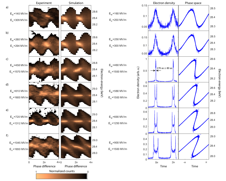
Fig. 2 shows experimental data, simulation results, retrieved time traces and phase space diagrams for various laser intensities in the modulator. The measured spectrograms include effects from both the modulator and analyzer, rendering a direct extraction of the electron time structure at the analyzer position difficult. For this reason, we compare the measured spectrograms with numerically obtained ones to indirectly measure the micropulse length. The numerical spectrograms are based on a finite difference time domain (FDTD) simulation of the optical nearfields inside of the nanophotonic structures lum , while the electron tracking was performed with a Runge-Kutta motion solver gpt . From the simulation results, we also obtain the electron density and the phase space distribution shown in the two rightmost columns in Fig. 2.
From top to bottom, the laser intensity in the modulator structure increases. In the first two cases, Fig. 2 a) and b), the laser intensity in the modulator is below the intensity needed to produce fully bunched electrons at the analyzer structure. Hence, the temporal focus of the micro-bunches lies after the center of the analyzer. For the parameters shown in Fig. 2 c), the laser intensity is almost ideally matched to the drift length so that the electron pulses are close to the minimal pulse duration. The onset of over-bunching is, however, already discernible. When we increase the laser intensity in the modulator even further [Fig. 2 d) - f)], the temporal focus shifts closer to the modulator, resulting in clear over-bunching at the position of the analyzer.
To find the best matching numerical spectrograms, we have simulated various parameter sets close to the experimental ones. This process and the concomitant pulse duration extraction are detailed in the supplemental material. Importantly, the length of the electron micro-bunch duration can not be directly inferred from features contained in the recorded spectrograms. This is because the relatively high energy spread induced in the modulator structure causes significant bunch evolution even in the analyzer structure since the temporal depth of focus is so narrow. A unique best matching solution for the spectrogram in Fig. 2 c) is found for these parameters: EM=, the incident field strength on the modulator structure, and EA=, the incident field on the analyzer. The resulting micro-bunch duration (full width at half maximum, FWHM) is . The error is derived from the comparison with adjacent simulation results. In the vicinity of our shortest measured micro-bunches, a variation of in the modulator results in a change of in the analyzer structure. Hence, we conservatively estimate the measurement error to be . An extensive sweep, which was performed with step sizes of for the modulator fields and for the analyzer can be found in the supplementary materials. Within this grid of simulations we can uniquely identify the simulated spectrum that matches the experiment best.
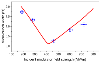
The experimentally achieved micro-bunch duration in the almost ideally bunched case of corresponds to just or 270 mrad of the optical driving period. In the simulation, we find that a minimal electron micro-bunch duration of should be feasible with the scheme and laser pulse parameters employed here (Fig. 3). With incident fields close to the damage threshold and shorter drift spaces, one might even consider reaching the single digit attosecond range. Simulations indicate that the structures used here would produce (FWHM) micro-bunches with an incident field on the modulator of after a drift space of , when the initial energy spread is small (< ). Note that spectra approaching a double hump structure resulting from a sinusoidal modulation have been observed Yousefi et al. (2019). This indicated that we can observe the required beam dynamics.
To summarize, we have demonstrated attosecond micro-bunch train generation with individual bunchlet durations as short as . Simulations show that the shortest micro-bunch duration with the current nanostructure could reach . Even shorter bunches can be achieved by reducing the drift section and using higher field strengths in the modulator section. The resulting micro-bunch trains could already be utilized to probe coherently pumped processes in a stroboscopic fashion. An increase in the available currents by orders of magnitude is straightforward by going to higher repetition rate laser sources (commercially available) and to better matched mini- or even micro-electron optics. Furthermore, advances in the fields of optical field-driven particle accelerators require sub-optical cycle-bunched electrons to be injected into the proper phase space region for the acceleration to be efficient and lossless. The precisely defined injection phase demonstrated here paves the way to matched injection into the acceptance of a scaleable DLA using technologies like the aforementioned alternating phase focusing. This enables to not only modulate electron energy, i.e. to have a beam with a big energy spread, comprised of accelerated and decelerated electrons, but to produce a net accelerated beam, where a substantial portion of the electrons is shifted to a higher energy with an energy spread significantly lower than that of a purely modulated beam. Our work will hence enable both new time-resolved electron-based imaging as well as building new and efficient optical particle accelerators. Similar results are reported in Black et al. (2019b).
Acknowledgements.
This work was funded by the Gordon and Betty Moore Foundation (GBMF) through Grant No. GBMF4744 ”Accelerator on a Chip International Program-ACHIP”, and BMBF via 05K16WEC and 05K16RDB.References
- Siwick et al. (2003) B. J. Siwick, J. R. Dwyer, R. E. Jordan, and R. J. D. Miller, “An atomic-level view of melting using femtosecond electron diffraction,” Science 302, 1382–1385 (2003).
- Baum et al. (2007) P. Baum, D.-S. Yang, and A. H. Zewail, “4d visualization of transitional structures in phase transformations by electron diffraction,” Science 318, 788–792 (2007).
- Morimoto and Baum (2018) Y. Morimoto and P. Baum, “Diffraction and microscopy with attosecond electron pulse trains,” Nat. Phys. 14, 252–256 (2018).
- Zewail and Thomas (2009) A. H. Zewail and J.M.b Thomas, 4D Electron Microscopy: Imaging in Space and Time (2009).
- Schliep et al. (2017) K. B. Schliep, P. Quarterman, J. P. Wang, and D. J. Flannigan, “Picosecond Fresnel transmission electron microscopy,” Appl. Phys. Lett. 110, 222404 (2017).
- Rubiano da Silva et al. (2018) N. Rubiano Da Silva, M. Möller, A. Feist, H. Ulrichs, C. Ropers, and S. Schäfer, “Nanoscale Mapping of Ultrafast Magnetization Dynamics with Femtosecond Lorentz Microscopy,” Phys. Rev. X 8, 031052 (2018).
- Berruto et al. (2018) G. Berruto, I. Madan, Y. Murooka, G. M. Vanacore, E. Pomarico, J. Rajeswari, R. Lamb, P. Huang, A. J. Kruchkov, Y. Togawa, T. LaGrange, D. McGrouther, H. M. Rønnow, and F. Carbone, “Laser-Induced Skyrmion Writing and Erasing in an Ultrafast Cryo-Lorentz Transmission Electron Microscope,” Phys. Rev. Lett. , 117201 (2018).
- Ackermann et al. (2013) S. Ackermann, A. Azima, S. Bajt, J. Bödewadt, F. Curbis, H. Dachraoui, H. Delsim-Hashemi, M. Drescher, S. Düsterer, B. Faatz, M. Felber, J. Feldhaus, E. Hass, U. Hipp, K. Honkavaara, R. Ischebeck, S. Khan, T. Laarmann, C. Lechner, Th Maltezopoulos, V. Miltchev, M. Mittenzwey, M. Rehders, J. Rönsch-Schulenburg, J. Rossbach, H. Schlarb, S. Schreiber, L. Schroedter, M. Schulz, S. Schulz, R. Tarkeshian, M. Tischer, V. Wacker, and M. Wieland, “Generation of coherent 19- and 38-nm radiation at a free-electron laser directly seeded at 38 nm,” Phys. Rev. Lett. 111, 114801 (2013).
- Kozák et al. (2018) M. Kozák, J. McNeur, N. Schönenberger, J. Illmer, A. Li, A. Tafel, P. Yousefi, T. Eckstein, and P. Hommelhoff, “Ultrafast scanning electron microscope applied for studying the interaction between free electrons and optical near-fields of periodic nanostructures,” J. Appl. Phys. , 023104 (2018).
- Kealhofer et al. (2016) C. Kealhofer, W. Schneider, D. Ehberger, A. Ryabov, F. Krausz, and P. Baum, “All-optical control and metrology of electron pulses,” Science 352, 429–433 (2016).
- Sciaini and Miller (2011) G. Sciaini and R. J. D. Miller, “Femtosecond electron diffraction: Heralding the era of atomically resolved dynamics,” Rep. Progr. Phys. 74, 096101 (2011).
- Zhao et al. (2018) L. Zhao, Z. Wang, C. Lu, R. Wang, C. Hu, P. Wang, J. Qi, T. Jiang, S. Liu, Z. Ma, F. Qi, P. Zhu, Y. Cheng, Z. Shi, Y. Shi, W. Song, X. Zhu, J. Shi, Y. Wang, L. Yan, L. Zhu, D. Xiang, and J. Zhang, “Terahertz Streaking of Few-Femtosecond Relativistic Electron Beams,” Phys. Rev. X 8, 021061 (2018).
- Baum and Zewail (2007) P. Baum and A. H. Zewail, “Attosecond electron pulses for 4d diffraction and microscopy,” Proc. Nat. Acad. Sci. USA 104, 18409–18414 (2007).
- Hilbert et al. (2009) S. A. Hilbert, C. Uiterwaal, B. Barwick, H. Batelaan, and A. H. Zewail, “Temporal lenses for attosecond and femtosecond electron pulses,” Proc. Nat. Acad. Sci. USA 106, 10558–10563 (2009).
- Kozák et al. (2018) M. Kozák, T. Eckstein, N. Schönenberger, and P. Hommelhoff, “Inelastic ponderomotive scattering of electrons at a high-intensity optical travelling wave in vacuum,” Nat. Phys. 14, 121–125 (2018).
- Kozák et al. (2018) M. Kozák, N. Schönenberger, and P. Hommelhoff, “Ponderomotive Generation and Detection of Attosecond Free-Electron Pulse Trains,” Phys. Rev. Lett. 120, 103203 (2018).
- Sears et al. (2008) C. M. S. Sears, E. Colby, R. Ischebeck, C. McGuinness, J. Nelson, R. Noble, R. H. Siemann, J. Spencer, D. Walz, T. Plettner, and R. L. Byer, “Production and characterization of attosecond electron bunch trains,” Phys. Rev. ST AB 11, 061301 (2008).
- Priebe et al. (2017) K. E. Priebe, C. Rathje, C. V. Yalunin, T. Hohage, A. Feist, S. Schäfer, and C. Ropers, “Attosecond electron pulse trains and quantum state reconstruction in ultrafast transmission electron microscopy,” Nat. Phot. 11, 793–797 (2017).
- England et al. (2014) R. J. England, R. J. Noble, K. Bane, D. H. Dowell, C.-K. Ng, J. E. Spencer, S. Tantawi, Z. Wu, R. L. Byer, E. Peralta, K. Soong, C.-M. Chang, B. Montazeri, S. J. Wolf, B. Cowan, J. Dawson, W. Gai, P. Hommelhoff, Y.-C. Huang, C. Jing, C. McGuinness, R. B. Palmer, B. Naranjo, J. Rosenzweig, G. Travish, A. Mizrahi, L. Schachter, C. Sears, G. R. Werner, and R. B. Yoder, “Dielectric laser accelerators,” Rev. Mod. Phys. 86, 1337–1389 (2014).
- Wootton et al. (2017a) K. P. Wootton, J. McNeur, and K. J. Leedle, “Dielectric Laser Accelerators: Designs, Experiments, and Applications,” Reviews of Accelerator Science and Technology 9, 105–126 (2017a).
- Peralta et al. (2013) E. Peralta, K. Soong, E. R. England, R. J.and Colby, Z. Wu, B. Montazeri, C. McGuinness, J. McNeur, K. J. Leedle, D. Walz, E. Sozer, B. Cowan, B. Schwartz, G. Travish, and Byer R. L., “Demonstration of electron acceleration in a laser-driven dielectric microstructure,” Nature 503, 91–94 (2013).
- Breuer and Hommelhoff (2013) J. Breuer and P. Hommelhoff, “Laser-based acceleration of nonrelativistic electrons at a dielectric structure,” Phys. Rev. Lett. 111, 134803 (2013).
- Wootton et al. (2017b) K. P. Wootton, D. B. Cesar, C. Lee, I. V. Makasyuk, J. Maxson, P. Musumeci, and R. J. England, “Dielectric laser acceleration and focusing using short-pulse lasers with an arbitrary laser phase distribution,” in AIP Conference Proceedings, Vol. 1812 (2017) p. 060001.
- Kozák et al. (2017) M. Kozák, J. McNeur, K. J. Leedle, H. Deng, N. Schönenberger, A. Ruehl, I. Hartl, J. S. Harris, R. L. Byer, and P. Hommelhoff, “Optical gating and streaking of free electrons with sub-optical cycle precision,” Nat. Commun. 8, 14342 (2017).
- McNeur et al. (2018) J. McNeur, M. Kozák, N. Schönenberger, K. J. Leedle, H. Deng, A. Ceballos, H. Hoogland, A. Ruehl, I. Hartl, R. Holzwarth, O. Solgaard, J. S. Harris, R. L. Byer, and P. Hommelhoff, “Elements of a dielectric laser accelerator,” Optica 5, 687–690 (2018).
- Black et al. (2019a) D. S. Black, K. J. Leedle, Y. Miao, U. Niedermayer, R. L. Byer, and O. Solgaard, “Laser-Driven Electron Lensing in Silicon Microstructures,” Phys. Rev. Lett. 122, 104801 (2019a).
- Niedermayer et al. (2018) U. Niedermayer, T. Egenolf, O. Boine-Frankenheim, and P. Hommelhoff, “Alternating-Phase Focusing for Dielectric-Laser Acceleration,” Phys. Rev. Lett. 121, 214801 (2018).
- Niedermayer et al. (2017) U. Niedermayer, O. Boine-Frankenheim, and T. Egenolf, “Designing a Dielectric Laser Accelerator on a Chip,” J. Phys.: Conf. Ser. , 012041 (2017).
- Breuer et al. (2014) John Breuer, Joshua Mcneur, and Peter Hommelhoff, “Dielectric laser acceleration of electrons in the vicinity of single and double grating structures-theory and simulations,” J. Phys. B: At. Mol. Opt. Phys 47 (2014).
- Leedle et al. (2015) K. J. Leedle, A. Ceballos, H. Deng, O. Solgaard, R. Fabian Pease, R. L. Byer, and J. S. Harris, “Dielectric laser acceleration of sub-100 keV electrons with silicon dual-pillar grating structures,” Optics Lett. 40, 4344–4347 (2015).
- Yousefi et al. (2019) P. Yousefi, N. Schönenberger, J. McNeur, M. Kozák, U. Niedermayer, and P. Hommelhoff, “Dielectric laser electron acceleration in a dual pillar grating with a distributed Bragg reflector,” Optics Lett. 44, 1520–1523 (2019).
- (32) https://www.lumerical.com/.
- (33) http://www.pulsar.nl/gpt/index.html.
- Black et al. (2019b) D. S. Black, U. Niedermayer, Y. Miao, O. Solgaard, R. L. Byer, and K. J. Leedle, “Generation, Acceleration, and Direct Measurement of Attosecond Electron Pulse Trains in Silicon Nanostructures,” submitted (2019b).