Moiré quantum chemistry: charge transfer in transition metal dichalcogenide superlattices
Abstract
Transition metal dichalcogenide (TMD) bilayers have recently emerged as a robust and tunable moiré system for studying and designing correlated electron physics. In this work, by combining large-scale first principle calculation and continuum model approach, we provide an electronic structure theory that maps long-period heterobilayer TMD superlattices onto diatomic crystals with cations and anions. We find that the interplay between moiré potential and Coulomb interaction leads to filling-dependent charge transfer between MM and MX regions several nanometers apart. We show that the insulating state at half-filling found in recent experiments on WSe2/WS2 is a charge-transfer insulator rather than a Mott-Hubbard insulator. Our work reveals the richness of simplicity in moiré quantum chemistry.
Following the recent discovery of correlated insulators and unconventional superconductivity in twisted bilayer graphene Cao et al. (2018a, b) and trilayer graphene-hBN heterostructure Chen et al. (2019a, b), artificial moiré superlattices have emerged as a new venue for realizing and controlling correlated electron phenomena. The moiré superlattices and natural solids differ greatly in the magnitude of characteristic length and energy. In solids, the average distance between electrons is typically comparable to atomic spacing in the order of and their kinetic and interaction energies are typically in the order of eV, while in moiré superlattices a mobile charge is shared by 1000–10000 atoms so that the characteristic length and energy scales are in the order of 10 nm and 10–100 meV respectively. Correspondingly, the quantum chemistry of natural solids involves complex intra-atomic and long-range interactions, while low-energy charge carriers in moiré superlattices only feel a long-period potential and interact with each other predominantly via the long-range Coulomb repulsion. Therefore, quantum chemistry can be simpler in moiré systems.
In twisted bilayer graphene, the emergence of strong correlation effects requires fine tuning to a magic twist angle, where the moiré energy bands become flattened Bistritzer and MacDonald (2011) and sensitive to microscopic details such as lattice relaxation Nam and Koshino (2017); Koshino et al. (2018); Carr et al. (2019); Yoo et al. (2019); Uchida et al. (2014); Van Wijk et al. (2015) and strain Bi et al. (2019). On the other hand, transition metal dichalcogenide (TMD) bilayers Wu et al. (2018, 2019); Tang et al. (2020); Regan et al. (2020) have a much simpler moiré band structure. In TMD heterobilayers such as WSe2/WS2, the valence moiré bands are simply formed by holes moving in a periodic moiré potential. Therefore, TMD superlattices provide a robust platform to study many-body physics with a highly tunable kinetic energy and local interaction strength.
Very recently, a correlated insulating phase has been observed in WSe2/WS2 at half-filling Tang et al. (2020); Regan et al. (2020) of the topmost valence moiré bands with a charge gap around 150K ( 10 meV) , and regarded as a canonical Mott-Hubbard insulator Hubbard (1963). In this scenario, the topmost moiré band is well separated from the rest; its charge distribution is tightly localized near the moiré potential minima, forming a triangular lattice. Strong on-site Coulomb repulsion suppresses double occupancy and creates an insulating gap at half-filling in the order of .
In this work, we identify a new energy scale associated with charge transfer between regions with different local stacking configurations in the moiré superlattice. When the energy cost of charge transfer is comparable to or smaller than the local Coulomb repulsion , the Mott-Hubbard description becomes inadequate. Instead, we show that a new type of correlated insulator emerges at half-filling, known as the charge-transfer insulator Zaanen et al. (1985). Using large-scale first-principles calculation, we obtain the parameters for various TMD heterobilayers and find that in WSe2/WS2 superlattice is comparable to the experimentally observed charge gapTang et al. (2020); Regan et al. (2020), whereas is much larger. We provide a theoretical description of the charge transfer phenomenon by introducing an effective honeycomb lattice model, in which the and sublattices correspond to “moiré cations” and “moiré anions” where charges are locally concentrated. We note that previous works on twisted bilayer graphene have shown the interaction induced charge redistribution within a local moire regionRademaker and Mellado (2018); Rademaker et al. (2019); Guinea and Walet (2018). Here the charge transfer we predict in TMD moiré superlattices takes place on the length scale of the moiré period ( 10 nm) and can be directly observed by scanning tunneling spectroscopy (STS).

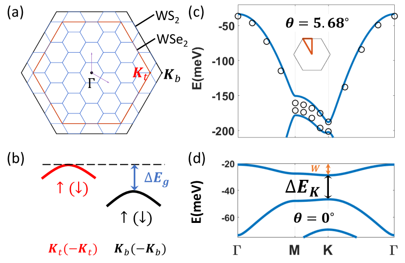
Continuum Model— We consider a heterobilayer TMD such as WSe2/WS2, with as the lattice constant of top (bottom) layer, and as the twist angle. The lattice mismatch leads to a moiré superlattice in Fig. 1, with superlattice constant where . As illustrated in Fig. 2b, the valence bands of two layers have a large band offset , which is listed for various TMD heterobilayers at zero twist angle in Table. S1. Given the large band offset, the low-energy moiré bands result from the spatial variation of valence band maximum of WSe2 due to the lattice mismatch with WS2 Zhang et al. (2017), which is described by a long-period moiré potential acting on holes in WSe2.
In this work, we study TMD heterobilayers with a small twist angle starting from AA stacking, where the metal atom and chalcogen atom of the top layer are aligned with metal atom and chalcogen atom at the bottom layer, respectively111Alternatively, AB stacking can be viewed as a rotation of top layer. There are three types of Wykoff positions in a moiré unit cell—hereafter referred to as MM, XM, MX, depending on the alignment of the metal atom (M) and chalcogen atom (X). As shown in Fig. 1a, at MM, the metal atoms on top and bottom layers are aligned, While at MX (XM), the metal atom on the top (bottom) layer is aligned with the chalcogen atom on the bottom (top) layer. In the long moiré wavelength limit , the valence band maximum varies slowly over the moiré unit cell, which can be expressed as the first-order harmonics with moiré wave vectors (i=1,2,3)Wu et al. (2018).
This is captured by the continuum model with
| (1) | |||||
| (2) |
where creates the holes and is the effective mass. From first principle calculation with the relaxed layer spacing(see Supplemental Material), we find the moiré valence bands within 200 meV are formed by pockets in WSe2. Owing to strong Ising spin-orbit coupling, valley indices are locked with spin (Xiao et al., 2012), and the two valleys are decoupled at long moiré wavelength limit. and are the only parameters associated with the magnitude and overall phase of the three lowest Fourier components of the moiré potential. When the moiré period is large, are intrinsic material properties independent of , which we hereafter refer to as moiré potential strength and moiré phase respectively.
| System | |||||
|---|---|---|---|---|---|
| WSe2/WS2 | 4% | 640 | 15 | 45∘ | 1.2 |
| WSe2/MoS2 | 4% | 940 | 11 | 40∘ | 1.2 |
| MoSe2/MoS2 | 4% | 630 | 9 | 42∘ | 1.3 |
| MoSe2/WS2 | 4% | 270 | 7 | 35∘ | 1.3 |
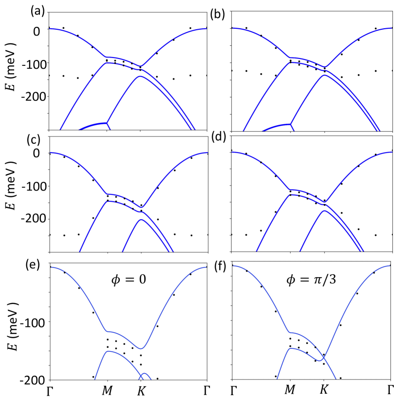
To obtain the values of , we first use the large-scale density functional theory (DFT) to calculate the moiré band structure of WSe2/WS2, WSe2/MoS2, MoSe2/MoS2, and MoSe2/WS2 at the commensurate angel , as shown in Fig. 2c. The spin-orbit coupling is included via DFTNaik and Jain (2018); Xian et al. (2020) as implemented in the Vienna Ab initio Simulation PackageKresse and Furthmüller (1996). The interaction between electrons and ionic cores is approximated by the projector augmented wave method, and the exchange-correlation potential was described by the Perdew-Burke-Ernzerhof generalized gradient approximationPerdew et al. (1996) with the vdW correction incorporated by the vdW-DF (optB86) functionals Klimeš et al. (2011). We assume rigid lattice along with in-plane directions and relax interlayer distance. Depending on the different vdW correction methods, the interlayer spacing is Angstrom. Throughout this range of interlayer distance, we find the moiré band structure is nearly identical.
We find the DFT band structure fits nicely with the continuum model (see Fig. 2c), and obtain from this fitting the material specific parameters and shown in Table. S1. For WSe2/WS2, meV and . Importantly, the moiré phase determines the energy landscape of moiré potential. This can be seen from at three -symmetric points (Wyckoff positions) and respectively. For , within one supercell there are one potential minimum (MM) and two maxima (MX and XM), while for , there are two minima (MM and MX) and one maximum (XM). The four TMD heterobilayers listed in Table. S1, WSe2/WS2, WSe2/MoS2, MoSe2/MoS2, and MoSe2/WS2, all belong to the parameter range , where the presence of two potential minima introduces new physics as we shall show below222WS2/MoS2 and WSe2/MoSe2 are discussed in Supplementary material..
In the following sections, we will study interaction effects in TMD heterobilayers in various regimes of and . We denote holes per supercell as the full filling and hole per supercell as the half-filling.
Charge-Transfer Phenomena— In this section, we use Hartree approximation to study the effect of Coulomb interaction on the charge distribution in twisted heterobilayer TMD with relatively large bandwidth and demonstrate the charge transfer phenomenon.
The Coulomb interaction including background effect is
| (3) |
where is the deviation of local hole density from the average (which is set by gate voltage), and is the Coulomb potential with dielectric constant , which controls the interaction strength. We approximate the Coulomb interaction by the mean-field Hatree potential self-consistently
| (4) |
and denotes the expectation value in mean-field ground state. As we assume the Hartree potential preserves all symmetries, can be written as Fourier series similar to Eq. (2), and the Coulomb interaction only renormalizes the band structure Guinea and Walet (2018); Cea et al. (2019).
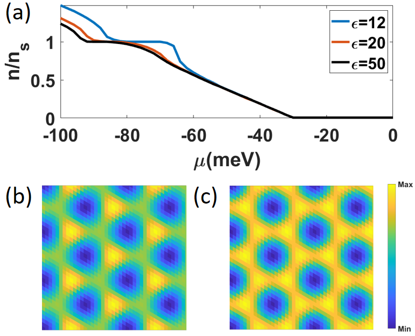
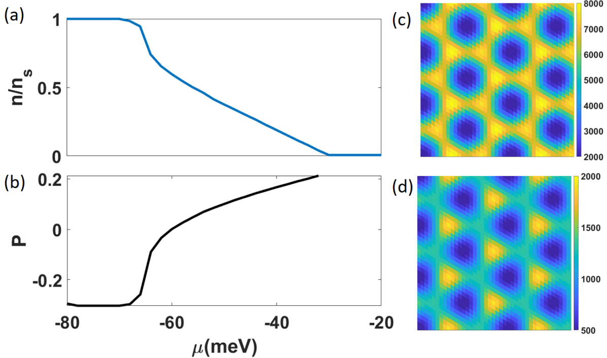
In Fig. 4a we plot the renormalized filling factor as a function of chemical potential in WSe2/WS2 heterobilayer at twist angle with different dielectric constants. At low fillings, the charge is always localized at MM spots. As we increase the filling, more holes will be accumulated and the repulsive interaction renormalizes the charge distribution to make it more homogeneous. Near half-filling , when the interaction is weak, the charge distribution remains at MM spots as shown in Fig. 4b. When the interaction is strong, charge transfer from MM to MX spots occurs and the corresponding charge distribution is shown in Fig. 4c.
In real space, the interaction-induced, filling-dependent charge transfer leads to a significant change of charge distribution on the scale of 10 nm, which can be detected by scanning tunneling spectroscopy (STS). In the energy domain, charge transfer affects band structure on the scale of 10 meV, which may be detected in angle-resolved photoemission spectroscopy and optical measurement of the exciton spectrum.
To go beyond the mean-field approximation, in the following we provide a theoretical description of charge transfer physics in TMD heterobilayer with a sufficiently large , where the moiré bandwidth is small compared to the moiré potential .
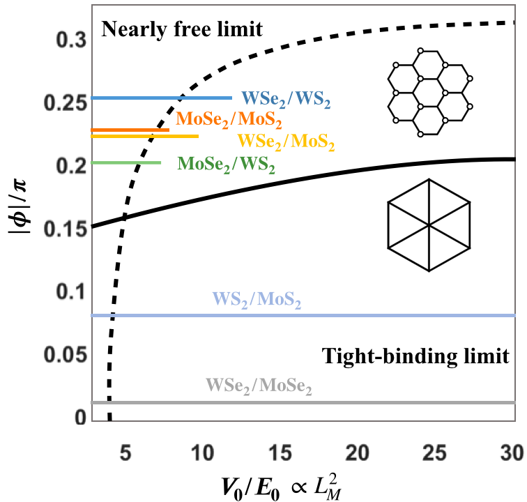
Tight-Binding Limit— We first introduce the moiré kinetic energy as , which increases with the twist angle as . When moiré potential is weak compared with kinetic term (nearly free limit), the first and second bands have a negative indirect gap (e.g. Fig. 2b). When moiré potential is much stronger than kinetic term (tight-binding limit), moiré bands become flat compared with band gaps (e.g. Fig. 2d). All untwisted heterobilayers listed in Table I belong to the tight-binding limit as shown in Fig. 3.
In the tight-binding limit, each potential minimum traps a set of local Wannier orbitals. The lowest-energy one is -orbital, and the next is doublet. The first moiré band is predominantly formed by orbitals at MM spots, which are global potential minimum in the parameter range of interest . The character of the second moiré band depends on . For , it comes from orbitals at MM spots. For and in a wide range of , it comes from -orbitals at MX spots that are local potential minima (see Fig. 2). The energy difference between orbitals in MX and MM spots defines a charge transfer gap .
By expanding around a potential minimum, we obtain the characteristic size of -orbitals in MM and MX spots from the harmoinc approximation
| (5) | |||
| (6) |
where only applies to . It is important to note that for large , is parametrically smaller than the moiré period. Therefore, the local Coulomb repulsion is the largest interaction energy, given by
| (7) |
with . In contrast, the interaction between nearest neighbors is proportional to and hence parametrically smaller than .
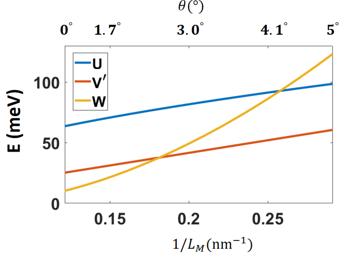
In Fig. S3 of the Supplementary Material we plot the bandwidth of the first moiré band and interaction energies of WSe2/WS2 at different twist angles. While decrease with in a power-law manner, is exponentially small in the tight-binding regime. For untwisted WSe2/WS2, we find nm, nm, nm and meV, meV, =8 meV, meV, meV.
Depending on the relative strengths of interaction energy, bandwidth, and charge transfer gap, we find three phases at half-filling.
(I) Metal: . The system is gapless. Under doping, additional charges are mainly localized at MM spots with -orbital symmetry.
(II) Mott insulator: . The insulating ground state has one hole per MM spot, and the charge gap is . When doped further, additional charges are mainly localized around MM spots. In this case, the triangular lattice Hubbard model is a good description Wu et al. (2018).
(III) Charge-transfer insulator: . The insulating ground state has one hole per MM spot, but the charge gap is . When further doped, additional charges are mainly localized at MX spots, thus resulting in charge transfer on moiré scale as the filling increases.
The insulating gap at half-filling inferred from thermal activation of resistivity is only around 10 meV Regan et al. (2020); Tang et al. (2020), which is significantly smaller than the estimated on-site repulsion meV assuming . (Note the distance from the sample to metallic gates is 20 nm so that screening has little effect on local repulsion ). However, the measured gap is comparable to the charge transfer gap meV. We thus conclude that the insulating phase at half-filling in untwisted WSe2/WS2 is likely a charge-transfer insulator, rather than a Mott-Hubbard insulator.
In order to capture the physics of charge transfer between MM and MX spots, we introduce an extended Hubbard model on the honeycomb lattice:
| (8) |
where denotes -orbital holes, for MX (MM) spots and denotes hopping. is the Coulomb repulsion between orbitals at site and , which includes both on-site repulsion , nearest-neighbor repulsion and etc. When there is strong screening from the metallic gates, interactions decay rapidly with the distance between sites.
At temperatures below the charge gap, double occupancy is strongly suppressed by the on-site repulsion . For the triangular lattice Hubbard model, the low-energy physics is described by the - modelSpalek (2007); Lee et al. (2006) with hopping and antiferromagnetic superexchange interaction between nearest neighbors. Magnetic susceptibility as a function of doping at various temperatures is shown in Supplementary Material. For charge-transfer insulators such as WSe2/WS2 described by the honeycomb lattice model (8), their magnetic properties call for future study.
The extended Hubbard model in honeycomb lattice has also been realized with cold atom in optical latticeJaksch et al. (1998); Hofstetter et al. (2002); Greiner et al. (2002); Gemelke et al. (2009); Soltan-Panahi et al. (2011). However, in cold atom systems, the lowest accessible temperature at present is on the order of hopping , which is much higher than the exchange interaction Mazurenko et al. (2017). In the TMD heterobilayer WSe2/WS2, the exchange energy is around meV and the corresponding temperature () is readily accessible for experiments.
In conclusion, we present a theory that maps the long period moiré system onto an atomic crystal with cation and anion and studies the correlated insulating behavior. We find that the interplay between moiré potential and interaction strength gives rise to charge transfer insulator in heterobilayer TMD, and opens the possibility of novel electronic states upon doping.
Acknowledgment
We thank Kin Fai Mak and Jie Shan for sharing their experimental results with us prior to publication, and Hiroki Isobe, Zhen Bi, Taige Wang, and Feng Wang for helpful discussions. This work is supported by DOE Office of Basic Energy Sciences under Award DE-SC0018945, N.Y. was partly supported by the U.S. Department of Energy, Office of Science, Basic Energy Sciences, under Award Number DE-SC0020149.
References
- Cao et al. (2018a) Y. Cao, V. Fatemi, A. Demir, S. Fang, S. L. Tomarken, J. Y. Luo, J. D. Sanchez-Yamagishi, K. Watanabe, T. Taniguchi, E. Kaxiras, et al., Nature 556, 80 (2018a).
- Cao et al. (2018b) Y. Cao, V. Fatemi, S. Fang, K. Watanabe, T. Taniguchi, E. Kaxiras, and P. Jarillo-Herrero, Nature 556, 43 (2018b).
- Chen et al. (2019a) G. Chen, L. Jiang, S. Wu, B. Lyu, H. Li, B. L. Chittari, K. Watanabe, T. Taniguchi, Z. Shi, J. Jung, et al., Nature Physics 15, 237 (2019a).
- Chen et al. (2019b) G. Chen, A. L. Sharpe, P. Gallagher, I. T. Rosen, E. J. Fox, L. Jiang, B. Lyu, H. Li, K. Watanabe, T. Taniguchi, et al., Nature 572, 215 (2019b), URL https://doi.org/10.1038/s41586-019-1393-y.
- Bistritzer and MacDonald (2011) R. Bistritzer and A. H. MacDonald, Proceedings of the National Academy of Sciences 108, 12233 (2011).
- Nam and Koshino (2017) N. N. Nam and M. Koshino, Physical Review B 96, 075311 (2017).
- Koshino et al. (2018) M. Koshino, N. F. Yuan, T. Koretsune, M. Ochi, K. Kuroki, and L. Fu, Physical Review X 8, 031087 (2018).
- Carr et al. (2019) S. Carr, S. Fang, Z. Zhu, and E. Kaxiras, Physical Review Research 1, 013001 (2019).
- Yoo et al. (2019) H. Yoo, R. Engelke, S. Carr, S. Fang, K. Zhang, P. Cazeaux, S. H. Sung, R. Hovden, A. W. Tsen, T. Taniguchi, et al., Nature materials 18, 448 (2019).
- Uchida et al. (2014) K. Uchida, S. Furuya, J.-I. Iwata, and A. Oshiyama, Physical Review B 90, 155451 (2014).
- Van Wijk et al. (2015) M. Van Wijk, A. Schuring, M. Katsnelson, and A. Fasolino, 2D Materials 2, 034010 (2015).
- Bi et al. (2019) Z. Bi, N. F. Yuan, and L. Fu, arXiv preprint arXiv:1902.10146 (2019).
- Wu et al. (2018) F. Wu, T. Lovorn, E. Tutuc, and A. H. MacDonald, Physical review letters 121, 026402 (2018).
- Wu et al. (2019) F. Wu, T. Lovorn, E. Tutuc, I. Martin, and A. MacDonald, Physical review letters 122, 086402 (2019).
- Tang et al. (2020) Y. Tang, L. Li, T. Li, Y. Xu, S. Liu, K. Barmak, K. Watanabe, T. Taniguchi, A. H. MacDonald, J. Shan, et al., Nature 579, 353 (2020).
- Regan et al. (2020) E. C. Regan, D. Wang, C. Jin, M. I. B. Utama, B. Gao, X. Wei, S. Zhao, W. Zhao, Z. Zhang, K. Yumigeta, et al., Nature 579, 359 (2020).
- Hubbard (1963) J. Hubbard, Proceedings of the Royal Society of London. Series A. Mathematical and Physical Sciences 276, 238 (1963).
- Zaanen et al. (1985) J. Zaanen, G. Sawatzky, and J. Allen, Physical Review Letters 55, 418 (1985).
- Rademaker and Mellado (2018) L. Rademaker and P. Mellado, Physical Review B 98, 235158 (2018).
- Rademaker et al. (2019) L. Rademaker, D. A. Abanin, and P. Mellado, arXiv preprint arXiv:1907.00940 (2019).
- Guinea and Walet (2018) F. Guinea and N. R. Walet, Proceedings of the National Academy of Sciences 115, 13174 (2018).
- Zhang et al. (2017) C. Zhang, C.-P. Chuu, X. Ren, M.-Y. Li, L.-J. Li, C. Jin, M.-Y. Chou, and C.-K. Shih, Science advances 3, e1601459 (2017).
- Xiao et al. (2012) D. Xiao, G.-B. Liu, W. Feng, X. Xu, and W. Yao, Physical review letters 108, 196802 (2012).
- Naik and Jain (2018) M. H. Naik and M. Jain, Physical review letters 121, 266401 (2018).
- Xian et al. (2020) L. Xian, M. Claassen, D. Kiese, M. M. Scherer, S. Trebst, D. M. Kennes, and A. Rubio, arXiv preprint arXiv:2004.02964 (2020).
- Kresse and Furthmüller (1996) G. Kresse and J. Furthmüller, Computational materials science 6, 15 (1996).
- Perdew et al. (1996) J. P. Perdew, K. Burke, and M. Ernzerhof, Physical review letters 77, 3865 (1996).
- Klimeš et al. (2011) J. Klimeš, D. R. Bowler, and A. Michaelides, Physical Review B 83, 195131 (2011).
- Cea et al. (2019) T. Cea, N. R. Waler, and F. Guinea, arXiv preprint arXiv:1906.10570 (2019).
- Spalek (2007) J. Spalek, arXiv preprint arXiv:0706.4236 (2007).
- Lee et al. (2006) P. A. Lee, N. Nagaosa, and X.-G. Wen, Reviews of modern physics 78, 17 (2006).
- Jaksch et al. (1998) D. Jaksch, C. Bruder, J. I. Cirac, C. W. Gardiner, and P. Zoller, Physical Review Letters 81, 3108 (1998).
- Hofstetter et al. (2002) W. Hofstetter, J. I. Cirac, P. Zoller, E. Demler, and M. Lukin, Physical review letters 89, 220407 (2002).
- Greiner et al. (2002) M. Greiner, O. Mandel, T. Esslinger, T. W. Hänsch, and I. Bloch, nature 415, 39 (2002).
- Gemelke et al. (2009) N. Gemelke, X. Zhang, C.-L. Hung, and C. Chin, Nature 460, 995 (2009).
- Soltan-Panahi et al. (2011) P. Soltan-Panahi, J. Struck, P. Hauke, A. Bick, W. Plenkers, G. Meineke, C. Becker, P. Windpassinger, M. Lewenstein, and K. Sengstock, Nature Physics 7, 434 (2011).
- Mazurenko et al. (2017) A. Mazurenko, C. S. Chiu, G. Ji, M. F. Parsons, M. Kanász-Nagy, R. Schmidt, F. Grusdt, E. Demler, D. Greif, and M. Greiner, Nature 545, 462 (2017).
- Mounet et al. (2018) N. Mounet, M. Gibertini, P. Schwaller, D. Campi, A. Merkys, A. Marrazzo, T. Sohier, I. E. Castelli, A. Cepellotti, G. Pizzi, et al., Nature nanotechnology 13, 246 (2018).
- Bauer et al. (2011) B. Bauer, L. Carr, H. G. Evertz, A. Feiguin, J. Freire, S. Fuchs, L. Gamper, J. Gukelberger, E. Gull, S. Guertler, et al., Journal of Statistical Mechanics: Theory and Experiment 2011, P05001 (2011).
- Koretsune and Ogata (2002) T. Koretsune and M. Ogata, Physical review letters 89, 116401 (2002).
Appendix A Commensurate structure
The lattice constants for MoS2, MoSe2, WS2 and WSe2 are 3.18818, 3.31579, 3.18719 and 3.31698 Angstrom respectivelyMounet et al. (2018). For bilayer with the same chalcogen atoms, the lattice mismatch is less than 0.1%, While for bilayer with different chalcogen atoms, the lattice mismatch is around 4%. To build a commensurate structure from two different monolayers with same type Bravais lattices, we consider a bilayer system, whose primitive vectors are denoted by and respectively. When the bilayer system is a commensurate superlattice with primitive vectors , we haveWu et al. (2018)
| (S1) | |||
| (S2) |
where are eight integers. These integers are determined by lattice mismatch between two layers (i.e. twist angle and strain) and also information of each layer (such as the anisotropy ratio). The most general way to determine these integers out of lattice information is through enumeration. We search all eight integers in a given range and compute corresponding lattice information for every given set of eight integers. When the calculated lattice information matches with the given one (up to some given precision), we then find the solution. In the following, however, we will discuss two special classes of superlattices where these eight integers have analytical solutions. When the two monolayers with threefold rotations, i.e. they are all triangular lattices, the integer matrices have to be conformal (i.e. a scalar times a rotation). Without loss of generality, let us assume and with , namely the unprimed layer is not rotated while the primed layer is rotated by angle along out-of-plane direction. Then the conformal matrices will have the following form
| (S3) | |||
| (S4) |
where are positive integers and are angles. Since each one of is effectively described by two parameters, we can write
| (S5) |
Furthermore, we want to consider first-order moiré pattern for simplicity, which is defined in terms of reciprocal vectors. Assume the reciprocal lattice vectors of two layers and the superlattice are , and respectively, then the first-order moiré pattern is defined by the conditions
| (S6) |
With this condition, it is found that , and hence the twist angle and lattice constant ratio between two layers are
| (S7) | |||
| (S8) |
and the superlattice vectors are
| (S9) | |||
| (S10) |
Here for TMDs with less than 0.1% lattice mismatch, we construct the commensurate moiré superlattice via twist the top layer with angles and . While for TMDs with lattice mismatch around 4%, the calculated twist angels are and .
Appendix B Details of the ab-initio calculation and parameter fitting
For MoSe2/WSe2 and MoS2/WS2 with nearly identical lattice constant, we fit the continue model parameters from the energy shift of band maxima from the relative shift of monolayer unit cellsWu et al. (2018), as shown in Table. S1. We note that the fitting from large-scale DFT as we have done in the main text would give different parameters, and leave the more realistic treatment such as lattice relaxation at the long moiré wavelength limit to future study.
For another four systems with lattice mismatch 4%, we fit the parameters of periodic potential and its phase factor directly from DFT band structures at various commensurate structures with different twist angles, a further calculation of DFT charge density distribution is performed to fix sign of the phase factor. We note that bilayer structures with twist angle fall into the gauge that pockets of monolayer unit cell fold to point of moiré BZ. The band structures of various TMD heterobilayers with unequal monolayer lattice constants are summarized in Fig. S1. Note the energy of pockets in MoSe2 is only lower by 120 meV compared with K pockets in MoSe2, which gives rise to the relatively flat second Moiré band around point in moiré BZ in Fig. S1 (a, b).
Since the charge transfer physics is dependent on the bandwidth and charge transfer gap , we choose the bandwidth of the first moiré band and the bandgap between first and second moiré band as the essential criteria for the fitting of continuum model parameters. As expected, the potential strength determines the moiré bandwidth, while the potential phase factor determines the bandgap at point in the moiré BZ. As shown in Fig. S1, we also list the band structure fitting with different phase factor for WSe2/WS2 heterobilayer, which shows a large bandgap in at and a degenerate point at for the first and second moiré band.
| System | |||||
|---|---|---|---|---|---|
| WSe2/MoSe2 | 370 | 8.14 | -4∘ | ||
| WS2/MoS2 | 360 | 6.52 | -13∘ |
Appendix C Fock term and Details of charge transfer
The full mean-field treatment of the Coulomb interaction also includes Fock decomposition , which results in the mean-field Hamiltonian with renormalized propagator , where is the bare propagator. We expect that the moiré potential and hence charge transfer physics discussed in this work would not be affected by Fock term too much.
We can introduce a dimensionless quantity to describe the charge imbalance between MM and MX spots
| (S11) |
and plot it as a function of chemical potential together with filling factor, as shown in Fig. S2a and b. As we can see, at low filling, the charge is mainly concentrated at MM spots , when doping increases, MM and MX spots first become balanced in terms of charge distribution , and then MX spots can have more charges than MM spots since repulsion at MX spots is weaker than MM. As explicit examples, we also plot charge distribution at different fillings and in Fig. S2 c and d respectively.
Appendix D Band structures, Coulomb interactions, and tight-binding models
In Fig. S3, we plot onsite repulsion , nearest-neighbor repulsion and bandwidth of WSe2/WS2 at different twist angles. All three energy scales decrease with decreasing angle (or equivalently increasing moiré wavelength ), but decreases faster than interactions.
As shown in Fig. 2, there are two regimes in the phase space spanned by moiré potential strength and moiré phase , where the second moiré bands are qualitatively different.
Triangular regime where the second and third moiré bands are from orbitals at MM spots and the corresponding tight-binding model is
| (S12) |
where denotes - and -orbital holes, and is MM spot. diag denotes onsite energy matrix, where denote the energy of and orbitals at MM spot respectively.
Honeycomb regime where the second moiré band is from orbitals at MX spots and the corresponding tight-binding model is
| (S13) |
where denotes -orbital holes, for MX (MM) spots and denotes hopping. And denotes the charge-transfer gap from MM to MX spots.
Appendix E Magnetic Properties
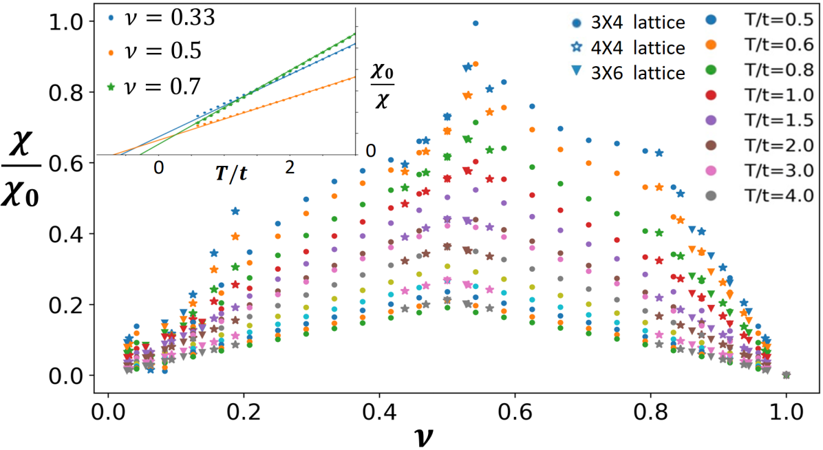
We also study the magnetic properties of - model in the triangular lattice. We performed ED (exact diagonalization) Bauer et al. (2011) on the triangular lattice model, and calculate temperature and filling dependent spin susceptibility.
From the Curie-Weiss law plot of susceptibilities in Fig. S4 inset, we found that Curie temperature moved towards zero when we increased the filling factor higher than half, indicating that antiferromagnetic correlation is reduced by doping. As shown in Fig. S4, in a wide temperature range, spin susceptibility is a non-monotonic function of filling factor with a maximal peak at optimal filling . Among them, at higher temperature the peak locates exactly at the half-filling , while at lower temperature , the susceptibility peak is shifted to above half-filling , in agreement with the result from high-temperature expansion studyKoretsune and Ogata (2002). These findings are consistent with the spin susceptibility of WSe2/WS2 heterobilayers inferred from optical spectroscopy under the magnetic field Tang et al. (2020).