An N-Path Filter with Multiphase PWM Clocks for Harmonic Response Suppression
Abstract
A switched-capacitor -path circuit can be employed for filtering an RF signal, as well as a passive downconverter. A known limitation of an N-path filter is that in addition to downconverting signals around the desired center frequency, the circuit also downconverts signals located around harmonics of the center frequency. An N-path filter that uses a PWM representation of a sinusoidal LO to mitigate harmonic downconversion is proposed in this work. Single-edge natural-sampling pulse-width modulated (PWM) clocks are used to drive the switches in the N-path filter. The potential for employing PWM for providing gain control is also described.
Index Terms:
Pulse-Width Modulation (PWM), N-path filter, Harmonic ResponseI Introduction
N-path filters frequency-translate the response of baseband filters to around an LO, thereby providing the frequency selectivity of a baseband circuit at a higher frequency [1]. Switch-based implementations of such filters have been demonstrated in recent literature e.g., [2][3][4][5]. N-path filters (Fig. 1) can provide a high effective quality factor, a high dynamic range and a tunable response, in addition to being scalable with process technology [6]. The filters allow for relaxing linearity at their input by attenuating blockers.

A typical CMOS implementation of a switch-based N-path filter employs non-overlapping pulse-based clocks of equal duty cycle of (1/), where is the frequency to which the baseband filter response is translated, and is the number of paths in the N-path filter (Fig. 1). For capacitive baseband loads ( in Fig. 1), an input signal at is effectively filtered by a bandpass response whose bandwidth is determined by , and . The N-Path filter also frequency translates an input signal at to a baseband signal at (nodes in Fig. 1).
With switching paths, input signals around are translated to around at the input node, which is termed harmonic-folding. This problem can be alleviated by increasing , which effectively pushes out the frequencies from where harmonic folding can occur farther out in frequency, compared to the desired signal input at . If combined with a band-limiting prefilter, the high-frequency components can be attenuated before they can fold in-band.
Another design challenge is that of harmonic response. In addition to , the baseband response is also translated to and conversely, an input signal located at , is translated to baseband, where for differential implementations, is odd. This can degrade performance in the presence of an interferer around , since the interferer after downconversion to baseband would overlap with the signal. An approach to reduce harmonic responses in an -path filter was shown in [7], which combined a harmonic-rejection front-end employing transconductor segments with a gain ratio with -path filters to suppress harmonic responses. -path filtering was implemented at the transconductor outputs. The filter does not relax linearity at the input of the transconductor.
Ideally, if sinusoidal LOs are used for frequency-translation, as theoretically analyzed in [1], the problem of harmonic response is avoided. However, a CMOS switch-based approach does not allow for directly employing a sinusoidal LO.
On the other hand, by employing PWM, a sinusoid can be represented by an equivalent switching waveform, which was demonstrated for providing harmonic rejection in a mixer in [8]. PWM is a signaling scheme, wherein the amplitude information of an analog signal is represented by the duty-cycle of a periodic discrete-level pulse train, that has a frequency that is significantly higher than the highest frequency of the analog signal [9]. Since the PWM signal is a discrete-level waveform, it can be easily combined with a switch-based –path filter, without the requirement for linear multipliers.
In this work, a PWM-based clocking scheme to reduce harmonic responses in a passive -path filter is proposed. The architecture, including clock-shaping are described in Section II. The approach also allows for gain control and a tunable input impedance match. Section III describes simulation-based results and the conclusion follows in Section IV.
II Overview of the Architecture
A PWM signal corresponding to a sinusoid and its spectrum are shown in Fig. 2. The PWM signal is generated by taking the difference of a continuous-time sinusoid of frequency , from a single-edge ramp waveform, and hard-limiting the difference, based on its polarity. The ramp is assumed to be periodic with a frequency of (period ), where . In general, . The closest significant harmonics in the PWM spectrum are located far from the component (Fig. 2).
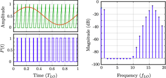
The PWM signal, , consists of a train of pulses, whose duty cycle varies in response to the sinusoidal LO of frequency . The PWM pulse-train exhibits a periodicity of , where , and thus can be expressed as a Fourier Series in the angular frequency , where .
| (1) |
The time-domain representation of can be determined by solving for the intersection points of the ramp waveforms with the sinusoid. The coefficients and can then be derived from . in Fig. 2, for a sinusoid amplitude of can be shown to have a DC component of 0.25, and a fundamental amplitude of .
The proposed architecture employs the above PWM sinusoids in the switching paths of Fig. 1. For , four PWM LOs that provide components with relative phase shift of are required. The PWM-LOs must be non-overlapping and contiguous so that one and only one load capacitor is connected to the input at any time. This avoids charge-sharing between the load capacitors, or an open-input, that can severely degrade the frequency response.
and PWM clocks are synthesized by comparing sine-waves of amplitude and frequency with quadrature phase-offset, in two consequent time-halves of one PWM pulse period (Fig. 3). This ensures that the and Q PWM pulses, and are non-overlapping. Further, PWM pulses are generated to synthesize out-of-phase components in the and paths each.
A sinusoid with phase is compared to a leading-edge ramp , for example, that is non-zero for . This provides the positive PWM-LO . Comparing a sinusoid of phase to a trailing-edge ramp, , in the same time then provides the complementary PWM-LO . and together span a time duration of . To generate the positive PWM-LO, , a sinusoid with phase is compared to a leading-edge ramp, , that is non-zero for . The sinusoid of phase , is compared to trailing-edge ramp that is non-zero in the same time window, to provide . and together span the full PWM pulse duration, and are non-overlapping. Since we assume, , 16 ramp pulses are applied to each phase of a full cycle of an sinusoid.

The waveform pairs and are not strictly out-of-phase, even though the phases of the frequency components at differ by since they are generated by different ramp signals (e.g, and ). Consequently, the baseband signals observed on the and , and similarly and paths, are not ideally out-of-phase.
The above issue is addressed by employing a transformer to split the input signal into differential signal components. Each transformer output is applied to a separate 4-path filter, and the outputs of each filter are combined at baseband, similar to a classical -path filter (Fig. 4). The PWM waveforms employed in the first -path filter are denoted by , while those in the second -path are given by .

The transformer provides a phase-split of 180∘ between its two outputs. Thus, 4-path filter outputs with clocks of opposite polarities need to be combined. Thus, for example, the path is combined with the path. All harmonic components of these two paths should be ideally out-of-phase. For this reason, both and employ the same ramp waveform in any given time window. The same argument is applicable for all other signal combinations , and .
In a differential sense, e. g., -, this clocking configuration applies a -level PWM switching between levels -1, 0 and 1, to the incident signal. This lacks an component, which improves quadrature performance.
It is possible to assign a single ramp to any one path of the filter (Fig. 3). While the differential LO pairs - and , are identical waveforms with relative phase, the common-mode components of the LOs, namely, + and +, are different. This makes the design sensitive to capacitive parasitics at the transformer outputs. To avoid this issue, an LO waveform shown in Fig. 5 is used, which alternates the ramp applied in each path. The 3-level differential PWM waveform is the same as the above case, but here the common-mode of the LO pairs is identical, and its current contribution in the presence of parasitics gets rejected as a common-mode at the transformer input ().
While the fundamental component of waveform moves to , this component appears as a common-mode in the spectrum of the 3-level PWM, and is rejected at the input, and significant PWM harmonics are still located around .

Since in each path, the frequency translation is performed by a sinusoid instead of a rectangular waveform, the harmonic responses observed in a classical -path filter are avoided. For , there is no significant harmonic response at harmonics from to (Fig. 2). An input series inductor is included in the design [4].
II-A PWM Pulse Generator
In the description above, we have assumed that the PWM pulses are generated by comparing a sinusoidal signal to a ramp in an ideal comparator. While this is theoretically possible, for applications requiring LOs in the tens to hundreds of MHz, this would imply the use of GHz-rate PWM ramps, which are difficult to implement. Additionally, this would also require comparators with gain-bandwidth products in the range of hundreds of GHz, which is impractical.
An alternative approach for generating high-frequency PWM clocks is described in [8] (Fig. 6). The approach uses a voltage-controlled delay line (VCDL) within a delay-locked loop (DLL), and can be employed here. An input clock with periodicity of and pulse width of is applied to the VCDL which provides delayed version at its output. The delayed clock is combined with the input to generate a pulse train , whose duty cycle is such that its average value is made equal to a pre-determined reference . For generating a PWM signal with 16 pulses, such as that in Fig. 4, 16 such pulse generators, with 16 corresponding s are employed. The outputs of the individual pulse generators are time-interleaved in steps of and combined through a simple logic operation, to generate a PWM signal corresponding to a sinusoidal LO [8].

The VCDL is a cascade of inverters, while the OP-AMP in the loop needs a very low gain-bandwidth product, since it is comparing a DC signal only. As such this is a low-power, and yet accurate approach to generate PWM pulses at GHz rates. PWM pulses that are equivalent to those generated by comparison of sinusoids to trailing-edge and leading-edge ramps can both be generated using this approach. This technique is mathematically equivalent to the ramp-based approach.
III Simulation results
Simulations of the proposed architecture of Fig. 4 are shown below. The basic principle is verified using ideal circuit switches, with specified on-state resistance. The simulations assume a series inductor of 35-nH although an inductor in the range of 20-40 nH is found to provide similar performance. A parasitic capacitance of 100-fF is assumed at the input. The design is also simulated and verified using switches implemented in a 65-nm commercial CMOS process, which includes the full-device model. The design employs PWM with frequency GHz and a sinusoidal LO with a fundamental frequency MHz. An ideal clocking network is employed in the simulations, however it is expected that clocking design similar to that previously demonstrated in silicon in [8] will be applicable to this work.

The harmonic responses at baseband of an N-path filter with fixed duty-cycle for , and PWM LOs in the configuration of Fig. 4 are shown in Fig. 7. The input frequency is swept within a MHz band around , for and the frequency-translated output at baseband is observed from around . The harmonic-response is observed to be significantly smaller for the PWM LOs.
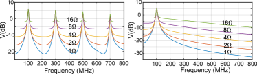
The RF response for the above two cases is compared in Fig. 8 for various values of the switch resistance . The filter with fixed duty-cycle LOs exhibits downconversion from all odd harmonics of , while the PWM-LO based filter shows a response only at . The response flattens with increasing [3]. The fixed duty-cycle filter simulations do not include an input inductor, since it degrades the harmonic response.

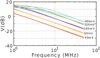
The response of the -path filter at the input node ( in Fig. 4) for the desired RF signal is shown in Fig. 9a, as a function of the effective sinusoidal LO amplitude (Fig. 4). A peak PWM ramp waveform of 1.2 V, and a sinusoidal DC level of 0.6 V is assumed. The peak of the bandpass response RF can be varied as a function of , which implies that the impedance match at the input can be controlled through . The maximum input voltage is observed for mV, while an optimal input match is observed for mV. Increasing to near the maximum value of V makes the minimum pulse width close to zero, which is difficult to employ in practice, due to rise and fall time limitations in the logic gates and drivers. On the other hand, for mV, the minimum PWM pulse widths have a duty-cycle in excess of 20%, which is achievable in modern CMOS technologies for in the GHz range. The baseband response ( in Fig. 4) is observed to vary linearly as LO amplitude (Fig. 9b) is increased and eventually saturate.
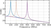
It is also possible to use sinusoids at multiples of in the PWM-LO filter, albeit at the expense of degraded harmonic folding. The fundamental bandpass response for various s with GHz is shown in Fig. 10 at MHz, for 2,4. The corresponding worst-case in-band harmonic folding are at levels of -65, -61 and -32 dB below peak, while considering an input band of up to 800 MHz. These arise from the image response of the filter and potentially can be reduced further.
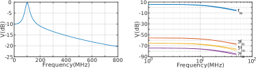
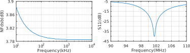
Simulation results employing MOS devices in a commercial 65nm CMOS process are shown in Fig. 11, which depicts the RF and baseband response, including harmonic response. Similar to using ideal switches, the design does not exhibit harmonic response. Noise figure and S11 performance are shown in Fig. 12.
IV Conclusion
An -path filter that employs multi-phase PWM clocks is proposed. Each path of the -path implements a sinusoidal LO, which effectively avoid the harmonic responses observed in -path implementations that employ rectangular pulses. The design can allow for a a passive-mixer based -path implementation. Performance parameters such as gain and bandwidth can be varied by changing the amplitude of the effective LO sinusoid. Simulation results using ideal switches and physical CMOS devices are presented.
References
- [1] L. E. Franks et al., “An Alternative Approach to the Realization of Network Transfer Functions: The N-Path Filter,” Bell System Technical Journal, vol. 39, no. 5, pp. 1321–1350, Sep. 1960.
- [2] B. W. Cook et al., “Low-power 2.4-GHz transceiver with passive RX front-end and 400-mV supply,” IEEE JSSC, vol. 41, no. 12, pp. 2757–2766, Dec. 2006.
- [3] A. Ghaffari et al., “A differential 4-path highly linear widely tunable on-chip band-pass filter,” in Proc. IEEE RFIC Symp., May 2010, pp. 299–302.
- [4] L. Duipmans et al., “Analysis of the Signal Transfer and Folding in N-Path Filters With a Series Inductance,” IEEE TCAS-1, vol. 62, no. 1, pp. 263–272, Jan. 2015.
- [5] G. Han et al., “A 0.3-to-1.3GHz Multi-Branch Receiver with Modulated Mixer Clocks for Concurrent Dual-Carrier Reception and Rapid Compressive-Sampling Spectrum Scanning,” in Proc. IEEE RFIC Symp., Jun. 2019, pp. 95–98.
- [6] M. Darvishi et al., “Design of Active N-Path Filters,” IEEE JSSC, vol. 48, no. 12, pp. 2962–2976, Dec. 2013.
- [7] Y. Xu et al., “A blocker-tolerant RF front end with harmonic-rejecting -path filter,” IEEE JSSC, vol. 53, no. 2, pp. 327–339, Feb 2018.
- [8] H. Kang et al., “A wideband receiver employing pwm-based harmonic rejection downconversion,” IEEE JSSC, vol. 53, no. 5, pp. 1398–1410, May 2018.
- [9] K. Nielsens, “A review and comparison of pulsewidth modulation (PWM) methods for analog and digital input switching power amplifiers,” in 102nd AES Convention, March 1997.