Moiré superlattice in a MoSe2/hBN/MoSe2 heterostructure: from coherent coupling of inter- and intra-layer excitons to correlated Mott-like states of electrons
Two dimensional materials and their heterostructures constitute a promising platform to study correlated electronic states as well as many body physics of excitons. Here, we present experiments that unite these hitherto separate efforts and show how excitons that are dynamically screened by itinerant electrons to form exciton-polarons, can be used as a spectroscopic tool to study interaction-induced incompressible states of electrons. The MoSe2/hBN/MoSe2 heterostructure that we study exhibits a long-period Moiré superlattice as evidenced by coherent-hole tunneling mediated avoided crossings between the intra-layer exciton with three inter-layer exciton resonances separated by meV. For electron densities corresponding to half-filling of the lowest Moiré subband, we observe strong layer-paramagnetism demonstrated by an abrupt transfer of all electrons from one MoSe2 layer to the other upon application of a small perpendicular electric field. Remarkably, the electronic state at half-filling of each MoSe2 layer is resilient towards charge redistribution by the applied electric field, demonstrating an incompressible Mott-like state of electrons. Our experiments demonstrate that optical spectroscopy provides a powerful tool for investigating strongly correlated electron physics in the bulk and pave the way for investigating Bose-Fermi mixtures of degenerate electrons and dipolar excitons.
Van der Waals heterostructures incorporating transition metal dichalcogneide (TMD) bilayers open up new avenues for exploring strong correlations using transport and optical spectroscopy. In contrast to similar structures in III-V semiconductors, these heterostructures exhibit possibilities for exotic material combinations, creation of Moiré superlattices exhibiting narrow electronic bandsYu2017 ; Wu2018a ; Wu2018 ; Ruiz-Tijerina2019 , and strong binding of spatially separated inter-layer excitonsFang2014 ; Rivera2015 ; Jauregui2018 ; Calman2018 ; Ciarrocchi2019 . Recently, ground-breaking transport experiments in twisted bilayer graphene demonstrated a fascinating range of strongly correlated electron physics in a single systemCao2018 ; Cao2018a ; Yankowitz2019 ; Liu2019 ; Sharpe2019 ; Lu2019 ; Serlin2019 : by varying the filling factor of the lowest energy Moiré from 0 to 1, the ground-state of the interacting electron or hole system could be reversibly changed from a superconductor for a large range of to a Mott insulator at () or a band insulator at . In fact, this system realizes a two-dimensional (2D) Fermi-Hubbard model on a triangular lattice with a fully-tunable electron density – a paradigmatic example of a strongly correlated electronic system with many open questions.
In parallel, optical spectroscopy in van der Waals heterostructures have revealed the prevalence of many-body hybrid light-matter states, termed exciton-polaronsSidler2017 ; Efimkin2017 , in the excitation spectra of electron or hole doped monolayers. Advances in material quality and device fabrication has lead to the observation of Moiré physics of non-interacting excitons in MoSe2/WSe2 Seyler2019 ; Tran2019 , MoSe2/WS2Alexeev2019 , and WS2/WSe2Jin2019 heterobilayers. Potential of this new system for investigating many-body physics was recently revealed in a remarkable demonstration of a long-lived inter-layer exciton condensateFogler2014 ; Wang2019 . Here, we describe experiments in a heterostructure incorporating a MoSe2/hBN/MoSe2 homobilayer that in several ways combine the principal developments in these two fields to demonstrate interaction-induced incompressible states of electrons. We provide an unequivocal demonstration of hybridization of inter- and intra-layer excitons mediated by coherent hole tunnelingDeilmann2018 ; Chaves2018 ; Ruiz-Tijerina2019 ; Alexeev2019 ; Gerber2019 between the two MoSe2 layers: the avoided crossings that we observe in optical reflection not only show the formation of dipolar excitons with a strong optical coupling but also reveal the existence of at least 3 Moiré bands of indirect excitons. We then demonstrate that intra-layer exciton-polaron resonances provide a sensitive tool to investigate correlated electronic states in the bulk. Equipped with this spectroscopic tool, we observe strong layer-paramagnetismZheng1997 ; Ezawa2000 and an incommpressible Mott-like state of electrons when each layer has half filling.
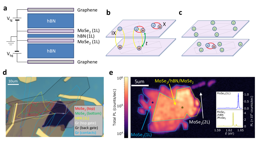
I Device structure and basic characterization
We show the schematic of the device structure in Fig. 1a. By using a double gate structure, we can control the electric field and the chemical potential of the device independently. Few-layer graphene serves as transparent gates, top and bottom hBN serve as gate insulators, and middle hBN (monolayer) serves as a tunnel barrier. The crystal axis of the layers are aligned to be close to 0 degree using the tear-and-stack techniqueKim2016 . Both layers are grounded via few-layer graphene contacts. Fig. 1d shows the optical microscope image of the device. Fig. 1b is a schematic image of a dipolar exciton formed by coherent coupling of inter-layer exciton (IX) and intra-layer exciton (X) via hole tunneling. Fig. 1c shows a schematic image of the electrons in a Moiré lattice probed by intra-layer exciton in low electron density regime.
Figure 1e shows a spatial map of total photoluminescence (PL) from the device. Here, both top and bottom gate voltages are kept at zero Volts.
We observe PL from regions with monolayer , but not from bilayer , where two flakes are in direct contact (the area around the point indicated by the white arrow in Fig. 1e). On the other hand, the /hBN/ area shows bright PL. This indicates that the heterostructure becomes a direct band gap system owing to the reduction of the inter-layer hybridization of the valence bands at the pointZhang2014 , due to the presence of monolayer hBN. Typical PL spectra of the monolayer and the /hBN/ area are shown in the inset of Fig. 1e: there are pronounced intra-layer exciton luminescence peaks in both areas. Even though the heterostructure is fabricated from a single layer using tear-and-stack technique, we observe two distinct intra-layer exciton peaks in the /hBN/ region. We observe that this strain-induced energy difference He2013 ; Conley2013 between the PL from the top and bottom layers varies across the the sample (see Supplementary Information S2).
II Coherent inter-layer hole tunneling and dipolar excitons
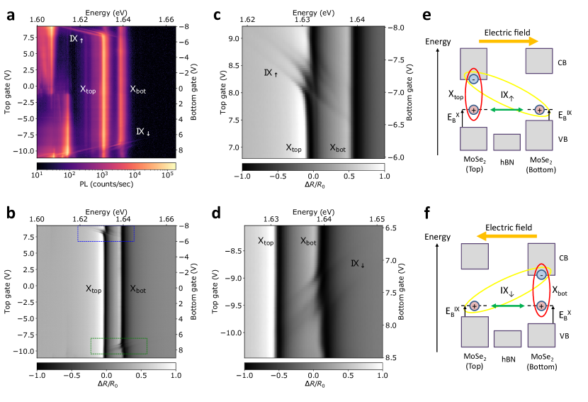
We first analyze the electric field () dependence of the elementary optical excitations of the /hBN/ section in the absence of itinerant electrons or holes. To this end, we scan the top and bottom gate voltages (along L4 indicated in Fig. 3c) together to change while keeping the homo-bilayer system in the charge neutral regime. The PL spectrum we thus obtain is depicted in Fig. 2a: using the top () and bottom () gate voltage dependence, we determine that the PL spectra around 1.632 eV and 1.640 eV stem from intra-layer exciton in top and bottom layer ( and ), respectively. For high values of depicted in the top and bottom parts of the color-coded PL spectrum, we observe PL lines with a strong dependence: we identify these PL lines as originating from inter-layer excitons with a large dipole moment leading to a sizeable Stark shift.
The spectra for positive (negative) regime corresponds to the inter-layer exciton () which has a hole in the bottom (top) layer and an electron in the top (bottom) layer. The associated dipole-moment of the inter-layer exciton changes its polarity for . By extrapolating the and PL lines and finding their crossing point, we estimate the energy difference between the inter- and the intra-layer exciton resonances at , which allows us to determine their binding energy difference to be 100 meV.
Figure 2b shows the differential reflectance () spectrum obtained for the same range of gate voltage scan as that of Fig. 2a. Here, , with and denoting the reflectance signal from the /hBN/ region, and background reflectance, respectively. In accordance with the PL data (Fig. 2a), we find and resonances around 1.632 eV and 1.640 eV, respectively. Moreover, for 7.5 V ( -7.5 V), we observe () hybridizing exclusively with (). Figures 2c and 2d show the magnified plots of the regions highlighted with blue and green dashed lines in Fig. 2b, confirming avoided crossing of an intra-layer exciton line with multiple inter-layer excitons. We first note that the observation of a sizeable reflection signal from away from the avoided crossing suggests that it is possible to resonantly excite long-lived inter-layer excitons in these structures. The hybridization of lines with , together with the lack of an avoided crossing with in Fig. 2c, unequivocally shows that avoided crossings originate exclusively from coherent hole tunneling schematically shown in Fig. 2e. Our observation, proving that the hole tunnel coupling is much larger than that of the electron, is consistent with the band alignment expected from first principle band-structure calculationsOzcelik2016 . This conclusion is also confirmed by the data depicted in Fig. 2d, where avoided crossing originates from coherent-hole-tunneling induced hybridization of and schematically shown in Fig. 2f.
One of the most remarkable features of the spectra depicted in Figs. 2c and 2d is the existence of multiple avoided crossings associated with three inter-layer exciton resonances separated in energy by meV. This inter-layer exciton fine-structure demonstrates the existence of a Moiré superlattice Yu2017 ; Wu2018 ; Ruiz-Tijerina2019 ; Alexeev2019 ; Seyler2019 ; Tran2019 ; Jin2019 , originating from a small twist angle between the two layers. The presence of an hBN tunnel barrier strongly suppresses the strength of the associated Moiré potential, rendering it sizeable only for the inter-layer excitons Yu2017 .
III Charge configuration detection by exciton-polaron spectroscopy
It is well established that presence of itinerant charges drastically alters the optical excitation spectrum Xu2014 . Recent theoretical and experimental work established that the modified spectrum originates from dynamical screening of excitons by electrons or holes Sidler2017 ; Efimkin2017 , that lead to the formation of a lower energy attractive polaron (AP) branch. Concurrently, the exciton resonance evolves into a repulsive polaron (RP) (see Supplementary Information S1). The particularly strong sensitivity of the RP resonance energy to changes in electron density renders it an ideal spectroscopic tool for monitoring, or sensing, the electron density in the same layer Back2017 ; Smolenski2019 . The strain induced resonance energy difference between and , ensuring different energies for the corresponding and , together with the much weaker sensitivity of () on in the bottom (top) layer, allows us to determine the charging configuration of the two layers simultaneously. Since we are predominantly interested in the low carrier density regime where the quasi-particle (bare-exciton) weight of the RP resonance is close to unity, we will refer to it as the exciton resonance.
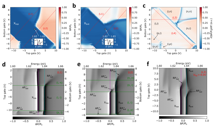
Figures 3a and 3b show the gate voltage dependence of at and , which correspond to the top () and bottom () intra-layer exciton resonance energy in the charge neutral regime, respectively. The inset to these figures show a line cut through the dispersive neutral exciton reflection spectrum, indicating the exciton energies at which we monitor . Since a small increase of from to cm-2 results in a change of from to , the blue areas in Figs. 3a and 3b correspond to the charge neutral regime of each layer. The red and white areas in turn, correspond to the electron or hole doped regime of each layer. This all-optical determination of the electrically resolved charge map of the bilayer provides an invaluable tool for monitoring the bulk properties of 2D materials which is not directly accessible in transport measurements.
To enhance the sensitivity of the charge map to the transition between the undoped and doped regimes and to visualize the charge configuration of both layers at the same time, we first evaluate the derivative of with respect to energy at and , and then overlay obtained for both layers. The resulting charge map, depicted in Fig. 3c, is closely reminiscent of the charging plateaus used to characterize gate-defined quantum dots Hanson2007 . Since is only sensitive to changes in , the blue regions in Fig. 3c correspond to the regime where the charge configuration changes, allowing us to clearly separate the regions (t,b) where the top or bottom layer is neutral (t=i or b=i), electron doped (t=n or b=n) or hole doped (t=p or b=p).
We show typical gate voltage dependence of in Fig. 3d and 3e which are obtained when the two gate voltages are scanned in a coordinated manner along the lines L1 and L2, indicated in Fig. 3a and 3b, respectively. In both plots, we confirm the emergence of the AP resonance and the associated blue shift of the exciton / RP energy around the charge configuration transition points, confirming the assignment obtained from in Fig. 3c.
In stark contrast to the case of monolayer (Supplementary Information S1), we find that the top (bottom) gate dependence obtained by fixing the bottom (top) gate voltage, is not monotonic because of the screening of the applied gate voltage when one of the two layers is already doped. The observed responsivity to the applied gate voltages is consistent with the interpretation that the lower (higher) energy exciton resonance at () is (). For example in Fig. 2b, by fixing = 0 V and sweeping from negative to positive, we find drastic change of around 2 V. On the other hand, by fixing = 0 V and sweeping from negative to positive, we find much less change of . From this asymmetry of the gate dependence, we can confirm that the resonance in Fig. 2b is originating from .
Figure 3f shows the gate voltage scan along L3, indicated in Fig. 3c, where we fixed at and scanned . By sweeping from negative to positive, we find that the bottom layer gets electron doped around , and then gets depleted by increasing further. This observation shows that electrons are transferred from the bottom layer to the top layer whilst electrons are introduced into the top layer and is kept unchanged. This counter-intuitive dependence shows up as the curving of the lines separating the charge configurations (n,i) and (n,n) in Fig. 3c. Similar inter-layer charge transfer behavior was previously observed in transport experiments in bilayer semiconductor systems Eisenstein1994 ; Larentis2014 ; Fallahazad2016 and was attributed to the negative compressibility. To the best of our knowledge, our experiments provide the first observation of negative compressibility, arising from dominance of intra-layer exchange interactions over kinetic energy, using optical spectroscopy.
IV Interaction induced incompressible states
The results we present in Sec. II establish the existence of a Moiré superlattice for inter-layer excitons. On the one hand, the underlying periodic modulation of the electronic bands should lead to Moiré subbands for electrons (holes) in the conduction (valence) band. On the other hand, the absence of coherent electron tunneling indicates that the resulting subbands in the top and bottom layers do not hybridize. Taking into account the relatively strong conduction-band spin-orbit coupling in MoSe2, the homobilayer system we are investigating realizes a rather unique system exhibiting flat bands with layer and valley-spin degree of freedom; while the degeneracy associated with the former can be tuned using a perpendicular electric field (), the latter can be controlled using a magnetic field (). Moreover, our observation of negative compressibility (Sec. III) indicates that the electron-electron interaction energy scale dominates over kinetic energy even at relatively high electron densities ( cm-2) where several Moiré bands in one layer are occupied. In this section, we explore electron correlation effects in the more interesting regime of low carrier densities by zooming in to the low- section of the charging map (Fig. 3c) where the (i,i), (i,n), (n,i) and (n,n) regions coalesce. The high sensitivity of the exciton/RP resonance energy, as well as the AP oscillator strength, to changes in electron density once again forms the backbone of our investigation.
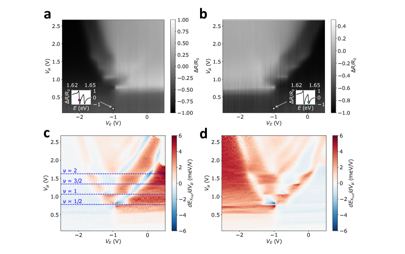
Figures 4a and 4b show the gate voltage dependence of differential reflectance close to the and resonance energy for at eV and eV, respectively. In these maps, a shift of the exciton resonance energy due to a change in is detected as a modification of the exciton reflectance. The specific choice of and , indicated by the magenta and cyan points in the insets of Fig. 4a and 4b, maximizes the sensitivity to . Instead of showing the reflectance map as a function of the top and bottom gate voltages, we now choose the horizontal and vertical voltage axes to be given by and . With this choice, vertical ( axis) and horizontal ( axis) cuts through the reflectance map leave and unchanged respectively, where denotes chemical potential.
Figures 4a and 4b show a periodic modulation of the RP differential reflectance as a function of , particularly in the low regime. Moreover, the modulation of the top and bottom layer reflectance are correlated and symmetric with respect to the V axis, indicating that for this value of , the energy detuning of the top and bottom layers is zero. To gain further insight into the structure of correlated changes, we first determine the excitonic resonance energy for the top and bottom layers ( and ) by fitting the reflectance spectrum with two dispersive Lorentzian lineshapes (see Supplementary Information S3) and then plot the derivative of and with respect to in Figs. 4c and 4d. The resulting map shows a remarkable checkerboard pattern that is complementary for the top and bottom layers. Since the blue shift of and resonance while increasing (positive and ) corresponds to filling of electrons in the top and bottom layer respectively, the complementary checkerboard like pattern indicates a layer by layer filling of electrons. Note that a similar diagram has been reported in layer resolved capacitance measurement of Landau lavels in bilayer grapheneHunt2017 .
The observed periodicity in Fig. 4 evidences the existence of Moiré subbands for electrons. In anticipation of the subsequent discussion, we define a layer filling factor (L = ”top” or ”bot” indicating top or bottom layer) so that corresponds to 1 electron per Moiré unit cell of a single layer, and a total filling factor as . From a capacitive model of our device, we determine that coincides with a remarkably low electron density of . At this low electron density, parameter, which describes the ratio of interaction energy to kinetic energy, is estimated to be . The density periodicity corresponds to a Moiré superlattice latice constant of by assuming a triangular superlattice. We indicate the values of corresponding to = 1/2, 1, 3/2, 2 with blue dashed lines in Fig. 4c.
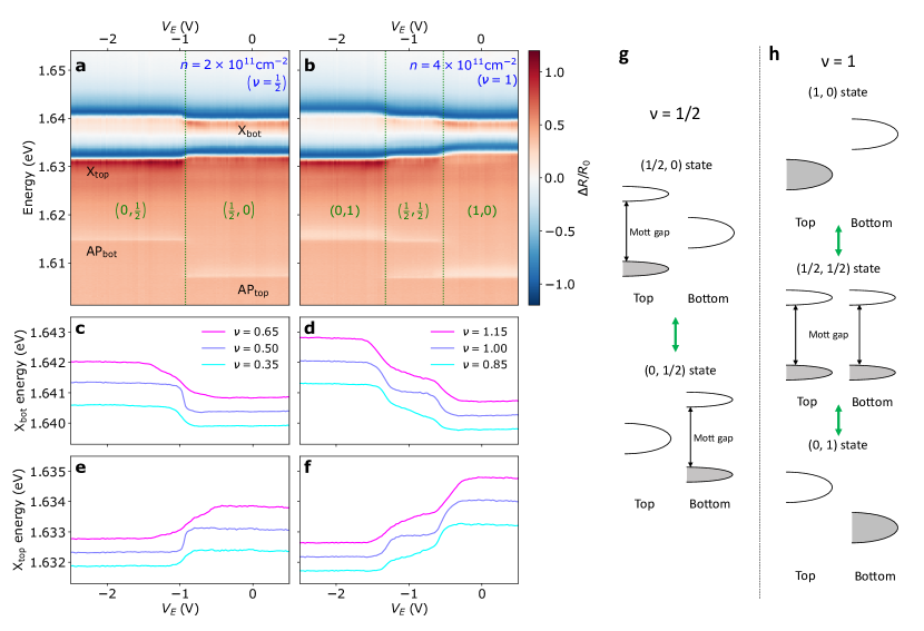
Figures 5a and 5b show the dependence of the differential reflectance spectrum for fixed where = 1/2 () and = 1 (), respectively. In Fig. 5a, we find an abrupt shift of exciton energy together with complete oscillator strength transfer between and . This shows that the electrons are completely and abruptly transferred from one layer to the other layer upon changing . Figs. 4c and 4e show the extracted and energies around = 1/2. Remarkably, the abrupt jump in excitonic resonance is pronounced at = 1/2, and smeared out for both lower ( = 0.35) and higher filling factors ( = 0.65). These measurements show that abrupt transfer of practically all of the electrons within the region we monitor optically is linked to the emergence of an interaction-induced incompressible state in the lowest Moiré subband at = 1/2 filling. As the filling factor is increased (decreased) towards , the electronic system shows an ever stronger layer-paramagnetism, due to enhanced role of interactions, but otherwise exhibits a continuous inter-layer transfer of electrons as a function of that would be expected from a compressible state. Close to , there is a phase transition to an incompressible state that can be accommodated either in the top or bottom layer (see Fig. 5g).
Figure 5b shows that for , the polaron reflectance spectrum as a function of is characterized by 3 plateau-like regions. We attribute the abrupt jumps in the excitonic resonance energy to the transition from = (0, 1), through (1/2, 1/2), to (1, 0) configurations (see Fig. 5h). This explanation is confirmed by the corresponding changes in the oscillator strength of the AP resonances of the top and bottom layers. In (1, 0) and (0, 1) configurations, we measure a reflectance signal either from or , consistent with full layer polarization. In the (1/2, 1/2) configuration, we find the oscillator strength of and to be identical and equal to half the value obtained under (1,0) for . The extracted excitonic resonance energy and around is shown in Figs. 5d and 5f, respectively. The plateau structure of the (1/2, 1/2) state with abrupt jumps in for V and V is clearly visible at , but is smeared out for both lower () and higher fillings (). We conclude that as the total is changed away from , both top and bottom layers become compressible, showing smooth changes in layers occupancy as a function of small values ( V). The emergence of the stabilized (1/2, 1/2) plateau at strongly suggests that there is mutual stabilization of the incompressible electronic state due to the inter-layer electron-electron interactions. If the or had been incompressible for , we would have observed corresponding plateaus in the the excitonic resonance reflection map. The reflectance data for higher fillings ( and ) are shown in the supplementary information (Fig. S5): in stark contrast to the (1/2, 1/2) configuration at , a plateau at the (1, 1) electron configuration is missing at filling, indicating that the state with the corresponding integer fillings is not sufficiently stabilized by the inter-layer interactions.
Finally, we emphasize that our identification of yielding half-filling of a single-layer Moiré subband is supported by our measurements at T: In Fig. S6 we observe that the plateau structure observed for under full valley polarization of electrons is identical to that observed for T, even though the total number of electronic states per Moiré subband is halved due to giant valley-spin susceptibility of electrons in MoSe2Back2017 . This observation shows that the incompressibility is determined by filling of each Moiré site by a single electron, irrespective of its degeneracy.
V Discussion
The experiments we describe in Sec. IV demonstrate the existence of Mott-like incompressible electronic states for half-filling of the lowest Moiré subband. Unlike prior reportsTran2019 ; Alexeev2019 ; Seyler2019 ; Jin2019 , our experiments are carried out for long Moiré superlattice latice constant of and parameter of . The weakness of the Moiré potential stemming from the hBN layer separating the two MoSe2 layers in turn ensures that the on-site interaction strength is comparable to, or possibly larger than, the depth of the Moiré potential. In this sense, the homobilayer system realizes a rather unique regime of the Fermi-Hubbard model where some of the expectations such as an antiferromagnetic ground-state need not be applicable.
In addition to establishing twisted TMD homo-bilayers as a promising system for investigating Mott-Wigner physicsImada1998 ; Camjayi2008 ; Zarenia2017 ; Wu2018 originating from strong electronic correlations, our experiments open up new avenues for exploring interactions between dipolar excitons and electrons confined to flat bands. In particular, the structure we analyzed could be used to realize and study Bose-Fermi mixtures consisting of degenerate electrons strongly interacting with an exciton condensate generated by resonant laser excitation. The phase diagram of such a mixutre is currently not fully understood Ludwig2011 but is expected to provide a rich playground for many-body physics, including but not limited to exciton-mediated superconductivity Little1964 ; Ginzburg1970 ; Laussy2010 ; Cotlet2016 .
Note added After completion of this work, we became aware of two manuscripts, arXiv:1910.08673 and arXiv:1910.09047, reporting similar results in a different material system.
METHODS
All , graphene, and hBN flakes are obtained by mechanical exfoliation of bulk crystals. The flakes are assembled together using the dry transfer techniqueWang2013 in an Ar filled glove box. The crystal axis of top and bottom layers are aligned to be close to 0 degree using tear-and-stack techniqueKim2016 . The metal electrodes to graphene layers are formed by Ti/Au (5 nm/145 nm). The contact to the bottom graphene gate is formed by Cr/Au (3 nm/147 nm) using the one-dimensional contact techniqueWang2013 by etching the hBN layer with reactive ion etching using as mixture gas.
The photoluminescence measurements were performed using a HeNe laser (633nm) as an excitation source. The reflectance measurements were performed using a single mode fiber coupled broadband LED with a center wavelength of 760nm and a bandwidth of 20nm. In both photoluminescence and reflectance measurements, we used a long working distance apochromatic objective lens with NA = 0.65 (attocube LT-APO/LWD/VISIR/0.65). All optical spectroscopy measurements have been performed at cryogenic temperature ().
References
- (1) Yu, H., Liu, G.-B., Tang, J., Xu, X. & Yao, W. Moiré excitons: From programmable quantum emitter arrays to spin-orbit–coupled artificial lattices. Sci. Adv. 3, e1701696 (2017).
- (2) Wu, F., Lovorn, T. & MacDonald, A. H. Theory of optical absorption by interlayer excitons in transition metal dichalcogenide heterobilayers. Phys. Rev. B 97, 035306 (2018).
- (3) Wu, F., Lovorn, T., Tutuc, E. & MacDonald, A. H. Hubbard Model Physics in Transition Metal Dichalcogenide Moiré Bands. Phys. Rev. Lett. 121, 026402 (2018).
- (4) Ruiz-Tijerina, D. A. & Fal’ko, V. I. Interlayer hybridization and moiré superlattice minibands for electrons and excitons in heterobilayers of transition-metal dichalcogenides. Phys. Rev. B 99, 125424 (2019).
- (5) Fang, H. et al. Strong interlayer coupling in van der Waals heterostructures built from single-layer chalcogenides. Proc. Natl. Acad. Sci. 111, 6198–6202 (2014).
- (6) Rivera, P. et al. Observation of long-lived interlayer excitons in monolayer MoSe2-WSe2 heterostructures. Nat. Commun. 6, 6242 (2015).
- (7) Jauregui, L. A. et al. Electrical control of interlayer exciton dynamics in atomically thin heterostructures (2018). eprint arXiv:1812.08691.
- (8) Calman, E. V. et al. Indirect excitons in van der Waals heterostructures at room temperature. Nat. Commun. 9, 1895 (2018).
- (9) Ciarrocchi, A. et al. Polarization switching and electrical control of interlayer excitons in two-dimensional van der Waals heterostructures. Nat. Photonics 13, 131–136 (2019).
- (10) Cao, Y. et al. Correlated insulator behaviour at half-filling in magic-angle graphene superlattices. Nature 556, 80–84 (2018).
- (11) Cao, Y. et al. Unconventional superconductivity in magic-angle graphene superlattices. Nature 556, 43–50 (2018).
- (12) Yankowitz, M. et al. Tuning superconductivity in twisted bilayer graphene. Science 363, 1059–1064 (2019).
- (13) Liu, X. et al. Spin-polarized Correlated Insulator and Superconductor in Twisted Double Bilayer Graphene (2019). eprint arXiv:1903.08130.
- (14) Sharpe, A. L. et al. Emergent ferromagnetism near three-quarters filling in twisted bilayer graphene. Science 365, 605–608 (2019).
- (15) Lu, X. et al. Superconductors, Orbital Magnets, and Correlated States in Magic Angle Bilayer Graphene (2019). eprint arXiv:1903.06513.
- (16) Serlin, M. et al. Intrinsic quantized anomalous Hall effect in a moiré heterostructure (2019). eprint arXiv:1907.00261.
- (17) Sidler, M. et al. Fermi polaron-polaritons in charge-tunable atomically thin semiconductors. Nat. Phys. 13, 255–261 (2017).
- (18) Efimkin, D. K. & MacDonald, A. H. Many-body theory of trion absorption features in two-dimensional semiconductors. Phys. Rev. B 95, 035417 (2017).
- (19) Seyler, K. L. et al. Signatures of moiré-trapped valley excitons in MoSe2/WSe2 heterobilayers. Nature 567, 66–70 (2019).
- (20) Tran, K. et al. Evidence for moiré excitons in van der Waals heterostructures. Nature 567, 71–75 (2019).
- (21) Alexeev, E. M. et al. Resonantly hybridized excitons in moiré superlattices in van der Waals heterostructures. Nature 567, 81–86 (2019).
- (22) Jin, C. et al. Observation of moiré excitons in WSe2/WS2 heterostructure superlattices. Nature 567, 76–80 (2019).
- (23) Fogler, M. M., Butov, L. V. & Novoselov, K. S. High-temperature superfluidity with indirect excitons in van der Waals heterostructures. Nat. Commun. 5 (2014).
- (24) Wang, Z. et al. Evidence of high-temperature exciton condensation in two-dimensional atomic double layers. Nature 574, 76–80 (2019).
- (25) Deilmann, T. & Thygesen, K. S. Interlayer Excitons with Large Optical Amplitudes in Layered van der Waals Materials. Nano Lett. 18, 2984–2989 (2018).
- (26) Chaves, A., Azadani, J. G., Özçelik, V. O., Grassi, R. & Low, T. Electrical control of excitons in van der Waals heterostructures with type-II band alignment. Phys. Rev. B 98, 121302 (2018).
- (27) Gerber, I. C. et al. Interlayer excitons in bilayer MoS2 with strong oscillator strength up to room temperature. Phys. Rev. B 99, 035443 (2019).
- (28) Zheng, L., Ortalano, M. W. & Das Sarma, S. Exchange instabilities in semiconductor double-quantum-well systems. Phys. Rev. B 55, 4506–4515 (1997).
- (29) Ezawa, Z. F. Quantum Hall Effects: Field Theoretical Approach and Related Topics (World Scientific, 2000).
- (30) Kim, K. et al. van der Waals Heterostructures with High Accuracy Rotational Alignment. Nano Lett. 16, 1989–1995 (2016).
- (31) Zhang, Y. et al. Direct observation of the transition from indirect to direct bandgap in atomically thin epitaxial MoSe2. Nat. Nanotechnol. 9, 111–115 (2014).
- (32) He, K., Poole, C., Mak, K. F. & Shan, J. Experimental Demonstration of Continuous Electronic Structure Tuning via Strain in Atomically Thin MoS2. Nano Lett. 13, 2931–2936 (2013).
- (33) Conley, H. J. et al. Bandgap Engineering of Strained Monolayer and Bilayer MoS2. Nano Lett. 13, 3626–3630 (2013).
- (34) Özçelik, V. O., Azadani, J. G., Yang, C., Koester, S. J. & Low, T. Band alignment of two-dimensional semiconductors for designing heterostructures with momentum space matching. Phys. Rev. B 94, 035125 (2016).
- (35) Xu, X., Yao, W., Xiao, D. & Heinz, T. F. Spin and pseudospins in layered transition metal dichalcogenides. Nat. Phys. 10, 343–350 (2014).
- (36) Back, P. et al. Giant Paramagnetism-Induced Valley Polarization of Electrons in Charge-Tunable Monolayer MoSe2. Phys. Rev. Lett. 118, 237404 (2017).
- (37) Smoleński, T. et al. Interaction-Induced Shubnikov–de Haas Oscillations in Optical Conductivity of Monolayer MoSe2. Phys. Rev. Lett. 123, 097403 (2019).
- (38) Hanson, R., Kouwenhoven, L. P., Petta, J. R., Tarucha, S. & Vandersypen, L. M. K. Spins in few-electron quantum dots. Rev. Mod. Phys. 79, 1217–1265 (2007).
- (39) Eisenstein, J. P., Pfeiffer, L. N. & West, K. W. Compressibility of the two-dimensional electron gas: Measurements of the zero-field exchange energy and fractional quantum Hall gap. Phys. Rev. B 50, 1760–1778 (1994).
- (40) Larentis, S. et al. Band Offset and Negative Compressibility in Graphene-MoS2 Heterostructures. Nano Lett. 14, 2039–2045 (2014).
- (41) Fallahazad, B. et al. Shubnikov-de Haas Oscillations of High-Mobility Holes in Monolayer and Bilayer WSe2 : Landau Level Degeneracy, Effective Mass, and Negative Compressibility. Phys. Rev. Lett. 116, 086601 (2016).
- (42) Hunt, B. M. et al. Direct measurement of discrete valley and orbital quantum numbers in bilayer graphene. Nat. Commun. 8, 948 (2017).
- (43) Imada, M., Fujimori, A. & Tokura, Y. Metal-insulator transitions. Rev. Mod. Phys. 70, 1039–1263 (1998).
- (44) Camjayi, A., Haule, K., Dobrosavljević, V. & Kotliar, G. Coulomb correlations and the Wigner–Mott transition. Nat. Phys. 4, 932–935 (2008).
- (45) Zarenia, M., Neilson, D. & Peeters, F. M. Inhomogeneous phases in coupled electron-hole bilayer graphene sheets: Charge Density Waves and Coupled Wigner Crystals. Sci. Rep. 7, 11510 (2017).
- (46) Ludwig, D., Floerchinger, S., Moroz, S. & Wetterich, C. Quantum phase transition in Bose-Fermi mixtures. Phys. Rev. A 84, 033629 (2011).
- (47) Little, W. A. Possibility of Synthesizing an Organic Superconductor. Phys. Rev. 134, A1416–A1424 (1964).
- (48) Ginzburg, V. L. THE PROBLEM OF HIGH-TEMPERATURE SUPERCONDUCTIVITY. II. Sov. Phys. Uspekhi 13, 335–352 (1970).
- (49) Laussy, F. P., Kavokin, A. V. & Shelykh, I. A. Exciton-Polariton Mediated Superconductivity. Phys. Rev. Lett. 104, 106402 (2010).
- (50) Cotlet, O., Zeytinoglu, S., Sigrist, M., Demler, E. & Imamoglu, A. Superconductivity and other collective phenomena in a hybrid Bose-Fermi mixture formed by a polariton condensate and an electron system in two dimensions. Phys. Rev. B 93, 054510 (2016).
- (51) Wang, L. et al. One-Dimensional Electrical Contact to a Two-Dimensional Material. Science 342, 614–617 (2013).
Acknowledgments
We acknowledge discussions with E. Demler, R. Schmidt, T. Smolenski, A. Popert, and P. Knüppel.
This work was supported by the Swiss National Science Foundation (SNSF) under
Grant No. 200021-178909/1, the Japan Society for the Promotion of Science (JSPS) Postdoctoral Fellowship for Research Abroad.
Author Contributions
Y.S. and I.S. carried out the measurements. Y.S. designed and fabricated the sample.
M.K. helped to prepare the experimental setup.
K.W. and T.T. grew hBN crystal.
Y.S., I.S. and A.I. wrote the manuscript.
A.I. supervised the project.
Competing interests
The authors declare no competing financial interests.
Additional information
Supplementary information for this paper is available online.
Correspondence and requests for materials should be addressed to A.I. (imamoglu@phys.ethz.ch).