Guiding Dirac fermions in graphene with a carbon nanotube
Abstract
Relativistic massless charged particles in a two-dimensional conductor can be guided by a one-dimensional electrostatic potential, in an analogous manner to light guided by an optical fiber. We use a carbon nanotube to generate such a guiding potential in graphene and create a single mode electronic waveguide. The nanotube and graphene are separated by a few nanometers and can be controlled and measured independently. As we charge the nanotube, we observe the formation of a single guided mode in graphene that we detect using the same nanotube as a probe. This single electronic guided mode in graphene is sufficiently isolated from other electronic states of linear Dirac spectrum continuum, allowing the transmission of information with minimal distortion.
Like a photon, an electron can be used as a carrier of information Bäuerle et al. (2018). However, there is a limited number of tools to control a single electron Zhao et al. (2015) and the simple fact of guiding it coherently in a solid, like an optical fiber for light, is a technological feat Williams et al. (2011); Rickhaus et al. (2015a). One-dimensional materials such as semiconducting nanowires naturally provide guidance for electrons, but in these materials, electrons can only be transmitted over short distances before losing its information Chuang et al. (2013). Another possibility is through the edge channel of a two-dimensional electron gas in the quantum Hall regime, but a large magnetic field is required for the channel to be a single mode Rickhaus et al. (2015b), which is crucial for the carried information not to be distorted during propagation.
An alternative approach, conceptually similar to an optical fiber Gloge (1971), is to use an electrostatic potential well on a two-dimensional electron gas to confine the movement of electrons along one direction (Fig. 1a) Zhang et al. (2009); Jompol et al. (2009); Hartmann et al. (2010); Wu (2011). Particularly, massless quasiparticles in graphene is an ideal platform for the realization of such electron guide. The quasi-relativistic linear energy dispersion in graphene allows the wavefunction of the Dirac fermions travel with minimal distortion. Furthermore, it has been demonstrated that high mobility Dean et al. (2010) allows electrons to be transmitted ballistically over several microns even at room temperature Mayorov et al. (2011). In addition, graphene can be encapsulated between thin dielectric layers of hexagonal-boron nitride (h-BN) Wang et al. (2013), providing tunable electrostatic potential on the scale of a few nanometers, without degradation of the mobility. Electrostatic gating has produced various electron-optical elements, including lenses with negative refractive index Chen et al. (2016) and filter-collimator switches Wang et al. (2019).
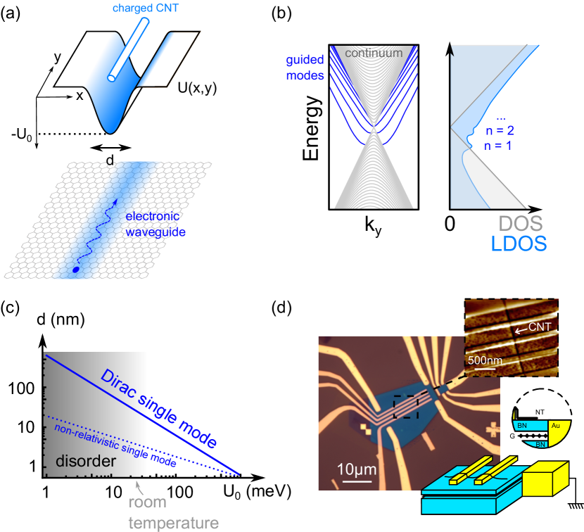
An ideal single mode electronic guide requires a deep potential well with a width much smaller than the wavelength of electrons in order to suppress scattering in the core of the waveguide Allen et al. (2016). The wavelength can reach around one hundred nanometers with experimentally accessible densities, and it is therefore crucial to be able to place extremely narrow gates close to the electron gas. The electronic modes generated by such a 1-dimensional (1D) potential well are manifested in the band structure of the graphene as branches similar to optical modes, which are separated from the continuum up to the energy that roughly corresponds to the depth of the potential well (Fig. 1b). Being isolated energetically, the guided modes are unlikely to mix with one another. Moreover, they are predicted to propagate ballistically over exceptional distance Shtanko and Levitov (2018). These modes form locally, at the center of the potential well, such that they do not affect the overall graphene density of states (DOS) but appear as resonances in the local density of states (LDOS) close to the LDOS minimum which indicates the position of the local Dirac point.
In this experiment, we use carbon nanotube (CNT) for creating 1D local gate to create a guiding mode in graphene by generating a potential well (Fig. 1a). The depth of the potential well can be continuously adjusted by a voltage difference applied between the CNT and the graphene. The width of the guided channel is roughly equal to the radius of the CNT, around 1 nm, plus the thickness of h-BN separating the CNT and graphene. The number of modes is then approximately given by the ratio , where is the Fermi velocity, and must, therefore, be of the order unity for a single mode waveguide Beenakker et al. (2009); Nguyen et al. (2009). In principle, this condition can be fulfilled for very wide and shallow potentials, but for the mode to be well-defined it is necessary that the potential depth is much greater than the fluctuations of chemical potential caused by the disorder. This limitation explains in particular why it is difficult to guide electrons in disordered graphene. For graphene encapsulated in h-BN, these fluctuations are on the order of a few meV Xue et al. (2011); Yankowitz et al. (2019). In order to obtain a single mode waveguide that is immune to disorder, the depth of the potential well, therefore, needs to be around a few tens of meV, which requires a width on the order of 10 nm (Fig. 1c). Such conditions are very hard to fulfill with standard techniques of nanofabrication but are conceivable using a gate made with a single-walled CNT in close proximity to graphene. We also note that the linear dispersion of Dirac fermion graphene is essential for our experiment. For non-relativistic electrons in semiconductors, the criterion to have a single mode is , where is the effective mass, leading to a much shallower potential well (meV) even for smaller width nm (Fig.1c).
An optical image of one of our devices is shown in Fig. 1d. Graphene is encapsulated between two layers of h-BN where the upper one is only a few nm thick and on which a CNT is deposited. Since the CNT diameter lies between 1 and 3 nm, and the thickness of our top h-BN layer is only a few nanometers, the characteristic width of the well is around 10 nm or less. We are thus able to drive the device into a single guided mode formed in graphene beneath the CNT. The graphene and CNT are both connected to their own electrodes which allows them to be independently controlled and measured. The length of the waveguide here is defined by the distance between electrodes connecting the CNT, i.e. 500 nm. The details of fabrication are given in the supplementary information SuppInfo .
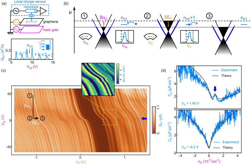
In addition to generating a potential well, the same CNT can also be used as a local probe to measure the graphene LDOS utilizing the capacitive coupling between CNT and the guided modes in the graphene. Here we operate the CNT as a single electron transistor (SET), i.e. a charge sensor Martin et al. (2008). Fig. 2a shows a schematic of the measurement scheme where the electrostatic potential of CNT SET can be controlled by both graphene gate voltage () and the global back gate voltage (). When connected to metallic electrodes and at sufficiently low temperature, a CNT generally enters the Coulomb blockade regime and becomes sensitive to external charges Laird et al. (2015). By measuring the conductance of the CNT as a function of the gate voltage or the potential applied to the graphene sheet , we observe a series of peaks corresponding to the different electronic energy levels of the CNT (Fig. 2a, bottom panel) each of which can contain one electron. These energy levels can individually be used as local probes sensitive to the electrostatic environment and therefore to the local charge density of graphene located below the CNT. The operational principle of these probes, inspired by direct measurements of Fermi energy performed in graphene and bilayer graphene Kim et al. (2012); Lee et al. (2014), is illustrated in Fig. 2b. When increasing the back gate potential , we fill the graphene band structure by increasing the number of carrier by with the corresponding change of Fermi energy . If the total electrochemical potential of graphene (electrostatic potential added to the Fermi energy ) exceeds the energy of one of the electronic states of the CNT, then the latter is also filled. Subsequently, we lower the graphene electrostatic potential with and therefore reduce the energy of all the electrons in graphene by an amount . If , adjusted by a change of the graphene bias , becomes lower than the energy of the same CNT electronic level, it consequently empties and goes back to its original state. By measuring the charge state of the CNT between each step, it is then possible to deduce the energy change corresponding a charge variation , where the charge of an electron. This procedure yields the local quantum capacitance of graphene
Note that the quantum capacitance at finite temperature is related to the compressibility of a mesoscopic system , which can be associated with the many body DOS Yu et al. (2013). Since capacitive coupling between graphene and CNT is strongly localized vicinity of the CNT, the measured is proportional to the LDOS of graphene underneath of the CNT. This quantity cannot be obtained with a global transport measurement. A remarkable aspect of this technique is that it provides an absolute measurement of quantum capacitance without any scaling parameters or adjustment of the origin of energies.
Fig. 2c shows the conductance of the CNT as a function of and . For this particular device, the h-BN spacer between CNT and graphene is only 4 nm thick, the measured peaks in the exhibit trajectories in the - plane that yield the evolution of the Fermi energy as we described above. The slope of these trajectories gives us directly the local quantum capacitance . When , the potential difference between the CNT and the graphene is small and, consequently, the potential well generated by the presence of the CNT is shallow. The LDOS measured (Fig. 2d) is then the one of bare graphene with a minimum at zero energy, following on the hole and electron sides. Note that denotes the global charge density of graphene since controls the charge density over the entire graphene sheet. With the minimum of LDOS being very close to , we deduce that the doping underneath the CNT is low, suggesting a locally low impurity levels. The minimum value of F.cm-2 also gives an estimation of the attainable minimal charge carrier concentration due to the charge puddle disorders cm-2.

As we generate a deeper potential well by increasing , the LDOS develops a more pronounced characteristic resonance, corresponding to a single guided mode. Compared to the measurement performed at , the minimum of quantum capacitance has shifted from the global charge neutrality point and towards the electron side (), as expected for a positive voltage applied on graphene while the CNT is maintained at ground potential. The resonance lies between this minimum and the global charge neutrality point of graphene (), a region where the doping caused by the potential well actually leads to a NPN junction configuration. The appearance of this resonance can be understood in the following manner: as a guided mode detaches from the Dirac cone, it generates a peak in the LDOS due to the 1D van Hove singularity appearing at the extrema of the single mode energy dispersion where is the wave vector along the CNT (see Fig. 3c). Our measurements are in excellent agreement with numerical tight-binding simulations Tworzydło et al. (2008); Hernández and Lewenkopf (2012) where the only fitting parameters are the depth and width of the potential well (see supplementary information SuppInfo ). Theory predicts the appearance of multiple successive modes that could give rise to additional resonances Jiang et al. (2017). However, due to presumably disorder induced broadening, unambiguously identifying multiple resonances is challenging within our experimental noise limit.
We observe a continuous evolution from bare graphene to a single mode waveguide as we tune the potential depth . Measurements of Fig. 3a shows that the graphene LDOS appears to be dramatically affected by tuning , by changing the potential difference between the CNT and graphene becomes non-zero. At low , it is already clear that the minimum corresponding to the Dirac point is less pronounced and that an asymmetry is formed between the electron and hole sides. This evolution, also predicted by numerical simulations (Fig. 3b), is due to the formation of closely packed guided modes whose branches are too close to the continuum, preventing the development of sharp resonances in the LDOS. Fig. 3c shows computed dispersion relation as a function of momentum along the CNT direction. A branch corresponding to the 1D guided mode gradually and continuously separates from the Dirac cone as increases Beenakker et al. (2009). For larger , we start to observe a resonance gradually increasing in amplitude and shifting from the charge neutrality point. This reflects the formation of a branch in the dispersion relation of graphene, which becomes increasingly more detached from the continuum. The curvature of this branch at its beginning becomes flat Beenakker et al. (2009) until it acquires a minimum located around , giving rise to a sharp resonance in LDOS. In the relativistic Dirac fermionic system, the 1D guide mode is expected to exhibit a potential strength threshold for the appearance of the first guided mode Nguyen et al. (2009); Hartmann and Portnoi (2014). While Fig. 3d suggests that indeed the appearance of a guided mode starts at finite , further experimental study with higher resolution requires to prove such threshold behavior unambiguously. Among all our devices, we were able to observe a single guided mode in the ones with upper h-BN that are 6 nm or thinner. In devices made with a thicker upper h-BN layer, from 10 to 100 nm, we were only able to observe the asymmetry between electron and hole sides but no resonance in the LDOS (see supplementary information). This experimental observation confirms that we cannot create a robust single mode electronic waveguide if the well is too wide and underlines the importance of the CNT for the realization of the single guided mode.
Technological applications for guided modes are possible if the energy separations between their branches and the continuum are sufficiently large. Indeed, to make the information transmission robust along the guide it is necessary to avoid processes that scatter electrons, leading to loss of information. For applications operating at room temperature, this energy must be well above thermal energy 25 meV. This separation is directly given by the energy position of the resonance with respect to the global Dirac point of graphene. Though our measurement technique does not work at room temperature since it relies on Coulomb blockade, we can see on the curve of Fig. 3d that we can control this energy continuously up to approximately 0.1 eV, well above thermal fluctuations at room temperature. This suggests that such guided modes could have great potentials to be used as novel electronic devices analogous to optical ones but where carriers of information are electrons rather than light. Additional measurements need to be performed at room temperature to confirm this hypothesis. Complementary measurements based on infrared nano-imaging Jiang et al. (2016), scanning tunneling spectrocopy Jung et al. (2011); Chae et al. (2012); Zhao et al. (2015), or planar tunneling spectroscopy Jung et al. (2017) with a 1D local gate created by a nanotube underneath the junction could also bring precious insight on the coherence, robustness and physical properties of these guided modes. More generally, guided modes in Dirac materials are also of interest for plasmonics applications Jiang et al. (2016); Basov et al. (2016); Ni et al. (2018), ultrafast electronic Huang et al. (2018), spintronics Khosravi et al. (2019) or to be used as test-beds for relativistic simulation Shytov et al. (2007); Wang et al. (2013b); Lu et al. (2019).
Acknowledgements.
We thank L. Levitov and J. Rodriguez-Nieva for discussion and M. O. Goerbig for his helpful reading of our manuscript. The major part of this work was supported by the Office of Naval Research (ONR N00014-16-1-2921). P.K acknowledges a partial support from the Department of Energy (DOE DE-SC0012260) for measurements. J.-D.P. acknowledges financial support from Ecole Polytechnique. K.W. and T.T. acknowledge support from the Elemental Strategy Initiative conducted by the MEXT, Japan and the CREST (JPMJCR15F3), JST.References
- Bäuerle et al. (2018) C. Bäuerle, D. C. Glattli, T. Meunier, F. Portier, P. Roche, P. Roulleau, S. Takada, and X. Waintal, Reports on Progress in Physics 81, 056503 (2018).
- Zhao et al. (2015) Y. Zhao, J. Wyrick, F. D. Natterer, J. F. Rodriguez-Nieva, C. Lewandowski, K. Watanabe, T. Taniguchi, L. S. Levitov, N. B. Zhitenev, and J. A. Stroscio, Science 348, 672 (2015).
- Williams et al. (2011) J. R. Williams, T. Low, M. S. Lundstrom, and C. M. Marcus, Nature Nanotechnology 6, 222 (2011).
- Rickhaus et al. (2015a) P. Rickhaus, M.-H. Liu, P. Makk, R. Maurand, S. Hess, S. Zihlmann, M. Weiss, K. Richter, and C. Schönenberger, Nano Letters 15, 5819 (2015a).
- Chuang et al. (2013) S. Chuang, Q. Gao, R. Kapadia, A. C. Ford, J. Guo, and A. Javey, Nano Letters 13, 555 (2013).
- Rickhaus et al. (2015b) P. Rickhaus, P. Makk, M.-H. Liu, E. Tóvári, M. Weiss, R. Maurand, K. Richter, and C. Schönenberger, Nature Communications 6, 6470 (2015b).
- Gloge (1971) D. Gloge, Applied Optics 10, 2252 (1971).
- Zhang et al. (2009) F.-M. Zhang, Y. He, and X. Chen, Applied Physics Letters 94, 212105 (2009).
- Jompol et al. (2009) Y. Jompol, C. J. B. Ford, J. P. Griffiths, I. Farrer, G. a. C. Jones, D. Anderson, D. A. Ritchie, T. W. Silk, and A. J. Schofield, Science 325, 597 (2009).
- Hartmann et al. (2010) R. R. Hartmann, N. J. Robinson, and M. E. Portnoi, Physical Review B 81, 245431 (2010).
- Wu (2011) Z. Wu, Applied Physics Letters 98, 082117 (2011).
- Dean et al. (2010) C. R. Dean, A. F. Young, I. Meric, C. Lee, L. Wang, S. Sorgenfrei, K. Watanabe, T. Taniguchi, P. Kim, K. L. Shepard, and J. Hone, Nature Nanotechnology 5, 722 (2010).
- Mayorov et al. (2011) A. S. Mayorov, R. V. Gorbachev, S. V. Morozov, L. Britnell, R. Jalil, L. A. Ponomarenko, P. Blake, K. S. Novoselov, K. Watanabe, T. Taniguchi, and A. K. Geim, Nano Letters 11, 2396 (2011).
- Wang et al. (2013a) L. Wang, I. Meric, P. Y. Huang, Q. Gao, Y. Gao, H. Tran, T. Taniguchi, K. Watanabe, L. M. Campos, D. A. Muller, J. Guo, P. Kim, J. Hone, K. L. Shepard, and C. R. Dean, Science 342, 614 (2013a).
- Chen et al. (2016) S. Chen, Z. Han, M. M. Elahi, K. M. M. Habib, L. Wang, B. Wen, Y. Gao, T. Taniguchi, K. Watanabe, J. Hone, A. W. Ghosh, and C. R. Dean, Science 353, 1522 (2016).
- Wang et al. (2019) K. Wang, M. M. Elahi, L. Wang, K. M. M. Habib, T. Taniguchi, K. Watanabe, J. Hone, A. W. Ghosh, G.-H. Lee, and P. Kim, Proceedings of the National Academy of Sciences 116, 6575 (2019).
- Allen et al. (2016) M. T. Allen, O. Shtanko, I. C. Fulga, A. R. Akhmerov, K. Watanabe, T. Taniguchi, P. Jarillo-Herrero, L. S. Levitov, and A. Yacoby, Nature Physics 12, 128 (2016).
- Shtanko and Levitov (2018) O. Shtanko and L. Levitov, Proceedings of the National Academy of Sciences 115, 5908 (2018).
- Beenakker et al. (2009) C. W. J. Beenakker, R. A. Sepkhanov, A. R. Akhmerov, and J. Tworzydło, Physical Review Letters 102, 146804 (2009).
- Nguyen et al. (2009) H. C. Nguyen, M. T. Hoang, and V. L. Nguyen, Physical Review B 79, 035411 (2009).
- Xue et al. (2011) J. Xue, J. Sanchez-Yamagishi, D. Bulmash, P. Jacquod, A. Deshpande, K. Watanabe, T. Taniguchi, P. Jarillo-Herrero, and B. J. LeRoy, Nature Materials 10, 282 (2011).
- Yankowitz et al. (2019) M. Yankowitz, Q. Ma, P. Jarillo-Herrero, and B. J. LeRoy, Nature Reviews Physics 1, 112 (2019).
- (23) See Supplementary Information for details of fabrication and numerical simulations, which includes Refs. Sfeir et al. (2004); Huang et al. (2005); Jiang and Fogler (2015).
- Sfeir et al. (2004) M. Y. Sfeir, F. Wang, L. Huang, C.-C. Chuang, J. Hone, S. P. O’Brien, T. F. Heinz, and L. E. Brus, Science 306, 1540 (2004).
- Huang et al. (2005) X. M. H. Huang, R. Caldwell, L. Huang, S. C. Jun, M. Huang, M. Y. Sfeir, S. P. O’Brien, and J. Hone, Nano Letters 5, 1515 (2005).
- Jiang and Fogler (2015) B.-Y. Jiang and M. M. Fogler, Physical Review B 91, 235422 (2015).
- Martin et al. (2008) J. Martin, N. Akerman, G. Ulbricht, T. Lohmann, J. H. Smet, K. von Klitzing, and A. Yacoby, Nature Physics 4, 144 (2008).
- Laird et al. (2015) E. A. Laird, F. Kuemmeth, G. A. Steele, K. Grove-Rasmussen, J. Nygård, K. Flensberg, and L. P. Kouwenhoven, Reviews of Modern Physics 87, 703 (2015).
- Kim et al. (2012) S. Kim, I. Jo, D. C. Dillen, D. A. Ferrer, B. Fallahazad, Z. Yao, S. K. Banerjee, and E. Tutuc, Physical Review Letters 108, 116404 (2012).
- Lee et al. (2014) K. Lee, B. Fallahazad, J. Xue, D. C. Dillen, K. Kim, T. Taniguchi, K. Watanabe, and E. Tutuc, Science 345, 58 (2014).
- Yu et al. (2013) G. L. Yu, R. Jalil, B. Belle, A. S. Mayorov, P. Blake, F. Schedin, S. V. Morozov, L. A. Ponomarenko, F. Chiappini, S. Wiedmann, U. Zeitler, M. I. Katsnelson, A. K. Geim, K. S. Novoselov, and D. C. Elias, Proceedings of the National Academy of Sciences 110, 3282 (2013).
- Tworzydło et al. (2008) J. Tworzydło, C. W. Groth, and C. W. J. Beenakker, Physical Review B 78, 235438 (2008).
- Hernández and Lewenkopf (2012) A. R. Hernández and C. H. Lewenkopf, Physical Review B 86, 155439 (2012).
- Jiang et al. (2017) Y. Jiang, J. Mao, D. Moldovan, M. R. Masir, G. Li, K. Watanabe, T. Taniguchi, F. M. Peeters, and E. Y. Andrei, Nature Nanotechnology 12, 1045 (2017).
- Hartmann and Portnoi (2014) R. R. Hartmann and M. E. Portnoi, Physical Review A 89, 012101 (2014).
- Jiang et al. (2016) B.-Y. Jiang, G. X. Ni, C. Pan, Z. Fei, B. Cheng, C. N. Lau, M. Bockrath, D. N. Basov, and M. M. Fogler, Physical Review Letters 117, 086801 (2016).
- Jung et al. (2011) S. Jung, G. M. Rutter, N. N. Klimov, D. B. Newell, I. Calizo, A. R. Hight-Walker, N. B. Zhitenev, and J. A. Stroscio, Nature Physics 7, 245 (2011).
- Chae et al. (2012) J. Chae, S. Jung, A. F. Young, C. R. Dean, L. Wang, Y. Gao, K. Watanabe, T. Taniguchi, J. Hone, K. L. Shepard, P. Kim, N. B. Zhitenev, and J. A. Stroscio, Physical Review Letters 109, 116802 (2012).
- Jung et al. (2017) S. Jung, N. Myoung, J. Park, T. Y. Jeong, H. Kim, K. Watanabe, T. Taniguchi, D. H. Ha, C. Hwang, and H. C. Park, Nano Letters 17, 206 (2017).
- Basov et al. (2016) D. N. Basov, M. M. Fogler, and F. J. G. d. Abajo, Science 354, aag1992 (2016).
- Ni et al. (2018) G. X. Ni, A. S. McLeod, Z. Sun, L. Wang, L. Xiong, K. W. Post, S. S. Sunku, B.-Y. Jiang, J. Hone, C. R. Dean, M. M. Fogler, and D. N. Basov, Nature 557, 530 (2018).
- Huang et al. (2018) W. Huang, S.-J. Liang, E. Kyoseva, and L. K. Ang, Semiconductor Science and Technology 33, 035014 (2018).
- Khosravi et al. (2019) F. Khosravi, T. Van Mechelen, and Z. Jacob, Physical Review B 100, 155105 (2019).
- Shytov et al. (2007) A. V. Shytov, M. I. Katsnelson, and L. S. Levitov, Physical Review Letters 99, 246802 (2007).
- Wang et al. (2013b) Y. Wang, D. Wong, A. V. Shytov, V. W. Brar, S. Choi, Q. Wu, H.-Z. Tsai, W. Regan, A. Zettl, R. K. Kawakami, S. G. Louie, L. S. Levitov, and M. F. Crommie, Science 340, 734 (2013b).
- Lu et al. (2019) J. Lu, H.-Z. Tsai, A. N. Tatan, S. Wickenburg, A. A. Omrani, D. Wong, A. Riss, E. Piatti, K. Watanabe, T. Taniguchi, A. Zettl, V. M. Pereira, and M. F. Crommie, Nature Communications 10, 477 (2019).
Supplementary Information for: Guiding Dirac fermions in graphene with a carbon nanotube
Austin Cheng , Takashi Taniguchi , Kenji Watanabe , Philip Kim, Jean-Damien Pillet
I Fabrication
I.1 Preparation of the circuit
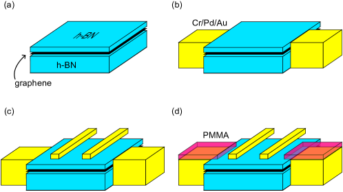
The sample shown in Fig. 1 of the main text is based on the initial preparation of an h-BN encapsulated graphene Wang et al. (2013) (Fig. S1a) on an n-doped silicon wafer with 285 nm SiO2. The thickness of the top h-BN layer is chosen between 4 and 100 nm and the bottom one around 20 nm. We use standard technique of e-beam lithography to design the electrodes contacting the graphene flake. We first expose the edges of the graphene flake by reactive ion etching through a resist mask and subsequently evaporate a metallic trilayer Cr(5nm)/Pd(15nm)/Au(5nm) through the same mask (Fig. S1b). A second step of lithography is then performed to design electrodes (same metallic trilayer) on top of the top h-BN layer. These electrodes are used to contact the carbon nanotube during the transfer step described at the end of this section (Fig. S1c). The sample is covered with a 100nm thick layer of resist (PMMA A4 495K) except for areas of interest where we want the nanotube to connect to electrodes. The resist helps on increasing the efficiency of the transfer of the carbon nanotube (Fig. S1d).
I.2 Growth of nanotubes and characterization
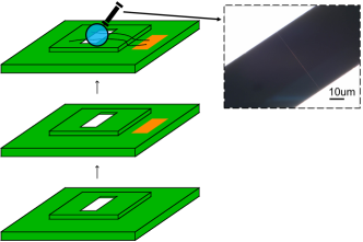
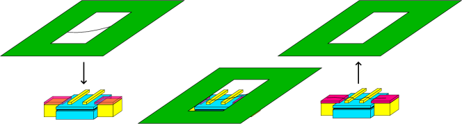
Carbon nanotubes are grown and characterized following the techniques described in Ref. Sfeir et al. (2004). They are grown on mm2 silicon chip with a slit in the center (see bottom of Fig. S2) using standard technique of chemical vapor deposition. A catalyst is deposited on one side of the slit (middle) such that carbon nanotubes grow suspended (top). One of these nanotubes, suspended over a slit that is 65m wide and 1cm long, is shown in the optical picture of Fig. S2. It is covered with 30 nm of Au, so it can be seen optically.
After growth, carbon nanotubes can be characterized using Rayleigh scattering. This identifies whether nanotubes are metallic or semiconducting as illustrated in Fig. S3. Moreover it also allows to measure the position of the carbon nanotube along the slit such that it can be aligned with the circuit for subsequent transfer.
I.3 Transfer
The incorporation of the carbon nanotube into the circuit is performed by mechanical transfer Huang et al. (2005) similarly to what is done to make h-BN encapsulated graphene. The slit is placed above the circuit in order to align the nanotube with the area of interest where we have designed dedicated electrodes. The slit is pressed on the sample as shown in Fig. S4. When we have good mechanical contact, we warm the chips up to 180∘C for 5 minutes in order to melt the resist that helps the nanotube transfer from the slit to the target chip. The two chips are then slowly separated after they have cooled down to room temperature.
II Quantum capacitance from measurements
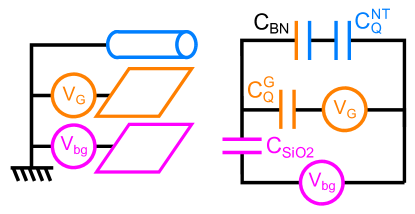
In Fig. S5, we describe our hybrid nanotube-graphene device as a network of capacitances including geometric and quantum capacitances in a fashion similar to what was done in Ref. Kim et al. (2012). This schematic is equivalent to the following set of equations
| (S1) |
where, as defined in the text is the voltage applied on the back gate, is the voltage applied on the graphene flake, is the number of carriers in the graphene flake (resp. nanotube), is the capacitance between the graphene flake and back gate (resp. nanotube) and is the Fermi energy of graphene. These equations can be obtained from an electrostatic description of the circuit where the total energy of the circuit is given by
where is the extra number of charge accumulated on the back gate, is the density of states of graphene (resp. nanotube) as a function of energy . The total energy contains five terms. The first two are the electrostatic energies of the two geometric capacitors formed, for the first one, by the back gate and the ensemble graphene-nanotube and, for the second one, by the graphene flake and the nanotube. The next two terms are the energies due to the fillings of electronic levels in the nanotube and in the band structure of graphene. The last two terms are the energy provided by the two voltage sources applying respectively a potential and on the graphene and back gate. This energy is minimum when and which, combined with the condition that since the circuit is a closed system, lead to the system of equations S1. Note that here we have used the fact that .
In practice, Eq. S1 simplify using the approximations , and that are essentially always valid since we apply tens of volts on the back gate while we apply only hundreds of mV on the graphene flake, the nanotube contains at best tens of electrons while the graphene flake contains tens of thousands of electrons, and the Fermi energy of graphene never exceeds a few hundreds of meV. By introducing the nanotube quantum capacitance , we end up with
| (S2) |
with . From these equations we see that, at a fixed number of charge in nanotube ( constant), we can deduce the number of charge in graphene and its Fermi energy for given values of and .
As a consequence, we can write that along a trajectory made by an electronic level of the nanotube (i.e. when the charge is fixed at half an integer) in the plane, we have
Since we have mesured independantly , we can deduce directly the quantum capacitance of graphene from the slope of these trajectories.
III Density of states calculation using a discretization of the massless Dirac equation
III.1 Dirac Hamiltonian
In order to describe our hybrid carbon nanotube-graphene devices, we use the two-dimensional massless Dirac Hamiltonian given by
where is the Fermi velocity, and the Pauli matrices. Due to the presence of the charged nanotube, the electrostatic potential landscape takes the shape of a potential well that is invariant along the axis of the nanotube (y-axis). For simplicity we choose a lorentzian potential though its precise shape actually depends on how the electrons of graphene screen the electric field generated by the nanotube. We write it as
where corresponds to the position of the nanotube along the x-axis, is the strength of the potential and is its width. The latter depends on the radius of the nanotube as well as the distance between nanotube and graphene given by the thickness of the h-BN between them. We have also tested a logarithmic potential , which corresponds to the potential generated by a one-dimensional wire in a parallel plane, but we have noticed no qualitative differences in the resulting density of states.
III.2 Discretized Dirac equations
In order to calculate the density of states in the graphene flake, we need to compute the eigenstates of this Hamiltonian , which obeys the massless Dirac equation
where are the eigenenergies. Since our problem is invariant along the direction, the operator can be replaced by a classical variable where is the projection of the wavevector along this axis. As a consequence, the solutions can be written as two-components spinors , which are plane waves along the y-axis.
We calculate and numerically using a discretization of the Hamiltonian over a lattice whose points are separated by a step . It is well known that a naive replacement of the derivative by its discret equivalent might not preserve the hermiticity of the Hamiltonian and cause a fermion doubling problem. To circumvent this problem, we use a scheme called Susskind discretization Tworzydło et al. (2008); Hernández and Lewenkopf (2012)
and
where and and is a relative integer such that for a flake of width . This means that we evaluate over the points of the lattice but at the midpoints. The discrete version of the Dirac equation is then written
| (S3) |
and
| (S4) |
and we choose the boundary conditions . Such boundary conditions results in the formation of states on the edge of the graphene flake, but it will not affect the local density of states below the nanotube.
Solving Eq. S3 and S4, we obtain branches of eigenenergies with corresponding eigenstates whose spinor components are and . In practice, this calculation is performed by first writing Eq. S3 and S4 in the following form
and then diagonalize numerically the matrix , which corresponds to the Hamiltonian. Here, we have defined a -components vector , and with the following matrices
and
In these expressions we have introduced matrices where is a matrix full of zeros, is the identity matrix, are matrices in which all the coefficients are zero except on the first upper (resp. lower) diagonal where all the coefficients are equal to 1, and is a diagonal matrix which refers to the the position along the x-axis.
Diagonalizing the matrix , we obtain the eigenvalues and the corresponding eigenstates . Note that in this approach, we suppose that the doping remains moderately small which consequently limits the screening effect. We therefore neglect the non-linear response of graphene to the electrostatic potential generated by the nanotube Jiang and Fogler (2015).
III.3 Global and local density of states calculations
The global density of states in graphene is given by
where the factor accounts for the spin degree of freedom and where we have introduced a phenomenological broadening for each electronic level of energy in order to smooth the density of states. In practice, we choose in our calculations, which roughly corresponds to the distance between two energy levels. The total density of states is obtained by summing over all the eigenenrgies of ( in total) for a given and then by summing over . Here we consider a graphene flake width and length such that we consider to be quantized quantized in steps of in the interval . In our calculations, we choose nm, and .
The local density of states below the nanotube is obtained in a similar fashion but taking into account the spatial distribution of the wavefunctions
where the matrix accounts for the small region below the nanotube over which the LDOS is measured. We choose this region to have the same width as the electrostatic quantum well created by the same nanotube such that can be written as
where we have assumed that the sensitivity of the nanotube decreases with distance following a lorentzian decay. Note that corresponds to the surface over which the nanotube measures the local density of states, which means that is a local density of states per unit area.
III.4 Fitting parameters and
In our simulation, we need only two fitting parameters to describe quantitatively the density of states we measure. The first one is the depth of the potential that we experimentally control with the voltage difference applied between the carbon nanotube and graphene . The second is the width of the potential which is roughly given by the radius of the nanotube plus the thickness of the h-BN spacer between nanotube and graphene. However, this only gives us an approximate value as the shape of the potential well generated by the nanotube will be affected by the screening of the graphene electrons. We obtain good agreement between theory and experiments using a width of 10 nm, that is to say in our simulations shown in Fig. 3b of the main part of the manuscript.
IV Devices with wider potential well
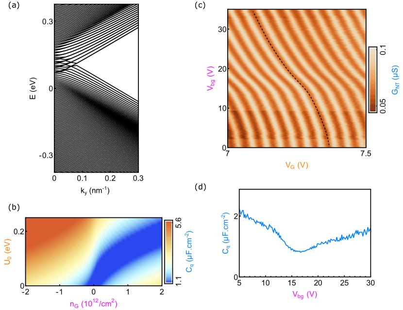
Fig. S6 shows simulations and measurements for devices with wider potential wells. The shown data come from a device with 30 nm thick h-BN separating the CNT and Gr. We observe qualitatively similar behaviors in devices with h-BN that is 10 nm or thicker.
The simulations are performed for a potential that is 100 nm wide. Fig. S6a shows the dispersion relation of Gr underneath the CNT when the potential is at eV. We observe that the branches are essentially indistinguishable from the continuum. Unlike the single mode which is well isolated from the continuum, these multi-modes can couple with one another as well as with the continuum easily, which makes them poorly guided.
Figure S6b shows the numerically calculated . We do not see resonances developing due to the fact that branches detaching from the continuum are too close from each other and the continuum. Figure S6c shows a carbon nanotube conductance measurement for the device around a high gate potential ( V). The trajectories of the conductance peaks form smooth S curves which represent the Dirac point and there are no “kinks” seen elsewhere. This signifies the absence of resonance in the density of states as shown in S6d.
However, we do observe an asymmetry developing between the elecron and hole sides and a smoothing of the Dirac point, meaning that the electric field generated by the nanotube affects the graphene density of states. The fact that we do not see resonances for wider potentials is in agreement with theory and an indication of the formation of several modes rather than a single guided mode. This provides further evidence that significantly sharp potential wells are required for the realization of a single mode electron guide.
References
- Wang et al. (2013) L. Wang, I. Meric, P. Y. Huang, Q. Gao, Y. Gao, H. Tran, T. Taniguchi, K. Watanabe, L. M. Campos, D. A. Muller, J. Guo, P. Kim, J. Hone, K. L. Shepard, and C. R. Dean, Science 342, 614 (2013).
- Sfeir et al. (2004) M. Y. Sfeir, F. Wang, L. Huang, C.-C. Chuang, J. Hone, S. P. O’Brien, T. F. Heinz, and L. E. Brus, Science 306, 1540 (2004).
- Huang et al. (2005) X. M. H. Huang, R. Caldwell, L. Huang, S. C. Jun, M. Huang, M. Y. Sfeir, S. P. O’Brien, and J. Hone, Nano Letters 5, 1515 (2005).
- Kim et al. (2012) S. Kim, I. Jo, D. C. Dillen, D. A. Ferrer, B. Fallahazad, Z. Yao, S. K. Banerjee, and E. Tutuc, Physical Review Letters 108, 116404 (2012).
- Tworzydło et al. (2008) J. Tworzydło, C. W. Groth, and C. W. J. Beenakker, Physical Review B 78, 235438 (2008).
- Hernández and Lewenkopf (2012) A. R. Hernández and C. H. Lewenkopf, Physical Review B 86, 155439 (2012).
- Jiang and Fogler (2015) B.-Y. Jiang and M. M. Fogler, Physical Review B 91, 235422 (2015).