Multi-frequency Shubnikov-de Haas oscillations in topological semimetal Pt2HgSe3
Abstract
Monolayer jacutingaite (Pt2HgSe3) has been recently identified as a candidate quantum spin Hall system with a 0.5 eV band gap, but no transport measurements have been performed so far on this material, neither in monolayer nor in the bulk. By using a dedicated high-pressure technique, we grow crystals enabling the exfoliation of 50-100 nm thick layers and the realization of devices for controlled transport experiments. Magnetoresistance measurements indicate that jacutingaite is a semimetal, exhibiting Shubnikov-de Haas (SdH) resistance oscillations with a multi-frequency spectrum. We adapt the Lifshitz-Kosevich formula to analyze quantitatively the SdH resistance oscillations in the presence of multiple frequencies, and find that the experimental observations are overall reproduced well by band structure ab-initio calculations for bulk jacutingaite. Together with the relatively high electron mobility extracted from the experiments ( cm2/Vs, comparable to what is observed in WTe2 crystals of the same thickness), our results indicate that monolayer jacutingaite should provide an excellent platform to investigate transport in 2D quantum spin Hall systems.
I Introduction
Two-dimensional (2D) quantum spin Hall insulators (QSHIs) constitute an important class of topological systems having a gapped insulating bulk and gap-less helical edge states that mediate transport at low energy kane_quantum_2005 ; kane_z2_05 ; Bernevig2006 ; Konig2007 ; Knez2011 ; Suzuki2013 ; Fei2017 ; Wu2018 . According to theory, these helical states are protected against elastic backscattering by time-reversal symmetry, so that edge conduction is predicted to occur in the ballistic regime over distances shorter than the inelastic scattering length. In reality, the material systems that have been identified experimentally as 2D QSHI –such as HgTe/CdTe Konig2007 ; Knez2011 ; Suzuki2013 ; Roth2009 ; Grabecki2013 ; Konig2013 ; Wu2018 and InAs/GaSb Konig2007 ; Knez2011 ; Suzuki2013 ; Roth2009 ; Grabecki2013 ; Konig2013 ; Wu2018 quantum wells– do not exhibit the expected, precisely quantized conductance: values close to per edge have been reported, with rather large sample-to-sample variations, as well as fluctuations as a function of applied gate voltage. Identifying the physical origin of these deviations is proving difficult, although several mechanisms have been put forwardKonig2007 ; Wu2006 ; Schmidt2011 ; Budich2012 ; Vayrynen2013 ; Wang2017 ; Novelli2019 . To progress, it is important to investigate experimentally a broader variety of 2D QSHI systems, in order to understand the influence of different microscopic parameters.
2D van der Waals (vdW) layered materials offer new opportunities, as illustrated by monolayers, whose predictedQian2014 2D QSHI nature has been confirmed by different experimentsFei2017 ; Tang2017 ; Wu2018 ; Shi2019 ; Cucchi2019 . Two-terminal edge conductance close to has been observed in hBN-encapsulated monolayersFei2017 , with subsequent work reporting a more precise quantization (albeit only for contact separation shorter than 100 nm Wu2018 ). Edge states have been directly detected by means of scanning tunneling microscopy Tang2017 and other types of local probes Shi2019 , and even the bands of monolayers could be mapped by means of angle-resolved photo-emission experiments (ARPES)Tang2017 ; Cucchi2019 . The 60-70 meV band-gap –significantly larger than in previous 2D QSHI systems– and the band structure were found to be in agreement with ab-initio calculationsQian2014 ; Tang2017 ; Cucchi2019 ; Zheng2016 . The improved conductance quantization, the larger band-gap, as well as the possibility to access directly the material with different experimental probes make an excellent candidate to study the physics of 2D QSHIs. These results also showcase the potential of 2D materials, and motivate the search for other atomically thin crystalsdresden_htz2_2018 ; olsen_z2ht_2019 ; Marrazzo2019 , providing even better platforms for experimental work.
Among these, jacutingaite –a vdW layered material with chemical formula – has been proposed to be of particular interest Marrazzo2018 . In its bulk form (see the crystal structure in Fig. 1a), jacutingaite is predicted to be a compensated semimetal hosting multiple electron and hole pockets that arise from nodal lines along which the valence (blue) and conduction (red) bands are degenerate in the absence of spin-orbit interaction (SOI) (see e.g. the KH line in Fig. 1b). SOI is, however, not negligible owing to the presence of heavy elements and lifts the degeneracy between valence and conduction bands (that remain separately two-fold degenerate owing to the combination of inversion and time-reversal symmetry), endowing the system with a non-trivial topology protected by crystalline symmetriesfacio_prm_2019 ; bansil_arxiv_2019 ; theory_jacu_2019 . The correspondingly expected surface states have been recently observed in ARPES measurementsexp_jacu_2019 , and found to be in remarkable good agreement with theoryfacio_prm_2019 ; bansil_arxiv_2019 ; theory_jacu_2019 . When the material thickness is reduced to that of an individual monolayer, jacutingaite is predicted to become a 2D QSHI realizing the original Kane-Mele modelkane_quantum_2005 ; kane_z2_05 , with a 0.5 eV band gap Marrazzo2018 (one order of magnitude larger than in ). Calculations also suggest that jacutingaite monolayers can be switched between a topological and a trivial insulating state, by applying electric fields Marrazzo2018 , as possibly achievable in 2D vdW heterostructures. If confirmed, all these predictions make monolayer jacutingaite an ideal platform to explore –and possibly control– 2D QSHI systems.
Despite a great interest in jacutingaiteMarrazzo2018 ; theory_jacu_2019 ; Cucchi2019 ; Kandrai2019 ; facio_prm_2019 ; bansil_arxiv_2019 ; Wu2019 , no transport measurements have been performed so far, neither on atomically thin layers nor on bulk, largely because growing high-quality crystals of sufficiently large size is challengingcabral_first_obs_08 . Here, we solve this problem by employing a high-pressure crystal synthesis technique to grow millimiter-sized crystals, which we exfoliate into thin layers (typically 50-to-100 nm thick) that enable the realization of multi-terminal devices for controlled transport experiments, and allow the quality of nano-fabricated structures to be assessed. The measured magnetoresistance indicates the presence of both electrons and holes, and exhibits pronounced Shubnikov-de Haas (SdH) oscillations with multiple frequencies. We discuss in detail how the Lifshitz-Kosevich (LK) formula can be adapted to the case of jacutingaite, to extract quantitative information. We find that the SdH oscillations are due to electrons, and that the observed frequencies originate from distinct pockets in the conduction band in overall good agreement with first-principles calculations. These results demonstrate that high-quality devices based on exfoliated layers can be produced (at least as good as WTe2 crystals of the same thicknessWang2015 ; Wang2016 ), a necessary step towards the investigation of the 2D QSHI state expected in monolayers that confirms the experimental potential of jacutingate.
II Methods
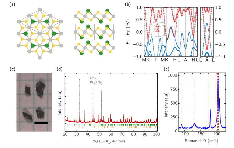
The small size () of existing jacutingaite crystals –extracted either from aggregates of platinum based mined minerals cabral_first_obs_08 , or from polycristalline powders grown in the laboratory jacutingaite_exp_12 – has so far prevented the exfoliation of thin layers to realize multi-terminal devices for controlled transport experiments. To grow larger high-quality crystals we have employed a high-pressure synthesis process that allows the growth of suitable materials in a few hours (see Supporting Information, SI, for details). The process results in a conglomerate a few millimeters in size, containing single crystals (see Fig. 1c) with dimensions up to . X-ray powder diffraction (XRD) shows the presence of crystals of two distinct compounds in the conglomerate, which we successfully identify as and from the corresponding series of diffraction peaks in Fig. 1d (the green and orange markers indicate the diffraction peaks for jacutingaite and ; the majority of crystals are jacutingaite, and 6-7 % of the material consists of PtSe2). To ensure that the material used for exfoliation is actually jacutingaite, we performed wavelength-dispersive X-ray spectroscopy (WDS) on each individual crystal and determine its chemical composition. We find the stoichiometry of the jacutingaite crystals to correspond to the nominal one within the sensitivity of our WDS system (approximately 1%), uniformly across the individual crystals. The identification of the jacutingaite crystals is confirmed by Raman spectroscopy measurements, which exhibit a series of active modes at characteristic wavelengths, in good agreement with values calculated for jacutingaite (see Fig. 1e red dashed lines and SI).
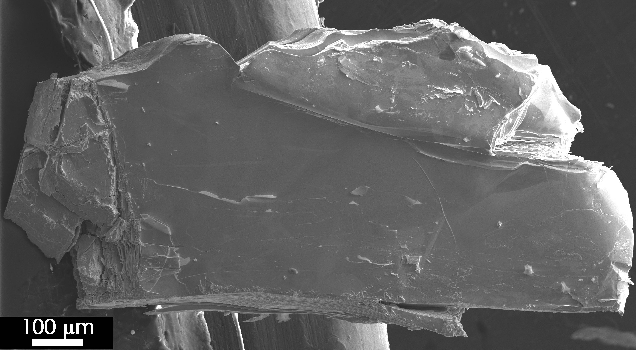
For the device fabrication we exfoliate thin jacutingaite layers and transfer them onto substrates covered with 300 nm . Conventional exfoliation procedures based on adhesive tape result in layers with lateral dimensions up to and thickness in the 50-100 range. Thinner crystals can also be found (down to few nanometers), but their lateral dimension () is normally too small to fabricate multi-terminal devices (as it is the case for virtually all other 2D materials, the availability of larger crystals –for which we are currently modifying the growth process– will likely yield larger exfoliated thin layers and eliminate this problem). Prior to contact deposition, we perform again Raman spectroscopy measurements, to ensure that the selected exfoliated layer is not an inclusion of , whose known Raman spectrum O_Brien_2016 is distinctly different from that of jacutingaite (see Fig. 1e). We found in all cases that exfoliation of jacutingaite crystals never shows any sign of PtSe2 inclusions, indicating that during the growth the two materials phase separate, i.e. the crystals in the as grown conglomerate are either jacutingaite or PtSe2. Contacts are prepared in a Hall-bar geometry (see top panel of Fig. 2a), using conventional nano-fabrication techniques (i.e., e-beam lithography, Ti/Au evaporation, and lift-off). As jacutingaite is a natural occurring mineral, the material is expected to be stable under ambient conditions, and indeed even the thinnest layers that we have exfoliated do not exhibit any visual sign of degradation, neither after several months of exposure to air nor after exposure to the chemicals commonly used in the device fabrication processes. For this reason, all the individual fabrication steps have been performed in air.
III Results and discussion
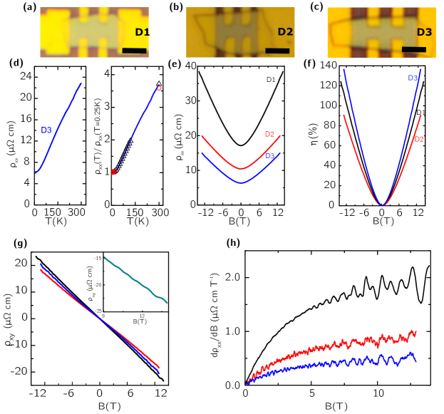
We measured three different devices (see figure Fig. 2a; labeled as D1, D2 and D3), based on layers that are respectively 90, 50 and 90 thick, all exhibiting similar behavior. The temperature dependence of the longitudinal resistivity of device D3, measured while slowly cooling the device from room temperature down to 250 mK, is shown in Fig. 2b (left panel). As expected for a semimetal, metallic behavior is observed, with decreasing linearly from 23 at room temperature to 6.2 at 15 K, below which saturation occurs similarly to what is observed for the resistivity of WTe2 crystals of comparable thickness Wang2015 . Finding that decreases upon lowering temperature indicates that down to K transport is limited by inelastic scattering and not by collisions with impurities, and provides a first indication of the electronic quality of our crystals. A very similar temperature dependence of the resistivity is observed for all the three devices measured, as can be seen in the right panel of Fig. 2b, which shows the resistivity normalized to its value at 250 mK . Data measured on the three devices (black, red and blue symbols for D1, D2 and D3 respectively) collapse onto a single curve, indicating that our exfoliated jacutingaite crystals are of similar quality, and exhibit a virtually identical residual resistivity ratio (3.71, 3.59, 3.69 for device D1, D2 and D3, respectively). Unexpectedly, in contrast with this behavior, the absolute value of the resistivity appears to exhibit significant differences in the three measured devices, as it may be inferred from the resistivity values measured at 250 mK –respectively , and in D1, D2, and D3 (see values in Fig. 2c). This seemingly large spread is mainly a consequence of the difficulty in determining the correct length-to-width ratio in our devices, which is affected by a sizable uncertainly because of the small dimensions of the exfoliated crystals (see Fig. 1a; indeed, the ratio does not depend on the device dimensions, which is why an excellent reproducibility is observed when looking at this quantity). Up to a smaller extent, the observed sample-to-sample deviations in absolute value of resistivity are also due to differences in the carrier mobility, as we discuss in more detail below.
The application of a perpendicular magnetic field up to 14 T, the highest field reached in our experiments (see Fig. 2c), causes the resistivity to increase. The corresponding magneto-resistance (MR; ), shown in figure Fig. 2d, reaches values ranging from 80 % to 140%, depending on the device. Notably, at high magnetic fields the MR deviates from the quadratic behavior commonly expected from classical dynamics of simple conductors, as depends linearly on . A linear MR has been reported previously in systems with topological properties and/or strong SOIXu2011 ; Liang2015 ; Shekhar2015 ; Leahy10570 , but the precise mechanism at work in jacutingaite remains to be determined.
The magnetic field dependence of the transverse resistivity is shown in Fig. 2e. With the exception of device D3 (that exhibits a small, but clear, non-linearity), the curve is essentially linear, with a negative slope indicative of a dominating electron contribution to transport. If interpreted in terms of a single type of charge carriers we find a spread of about 20% in the density values extracted from different devices: , and for D1, D2 and D3. Such a spread (as well as the fact that these values are twice laerger than what is expected from ab-initio calculations, ) cannot be attributed to unintentional doping due to impurities, since this explanation would require impurity concentrations reaching up to 5%. Such a concentration would not only have been detected in the WDS characterization of the material (see above), but would also cause a very short electronic mean free path, incompatible with the presence of the well-defined SdH conductance oscillations discussed below.
Finding inconsistencies when attempting to interpret the Hall data in terms of a single type of charge carrier is not surprising, because jacutingaite is predicted to be a compensated semimetal with an equal density of electrons and holes. Under the simplifying assumption that only one family of electrons and one family of holes are present, the expression for the Hall slope becomes ziman1972principles ( and are the hole and electron mobility). This expression naturally explains the larger densities extracted above, because –if the Hall slope is interpreted in terms of only electrons– a larger value of is obtained as compared to the actual one since . To account for the observed difference in Hall slopes it suffices that the ratio varies by a factor of 0.5 –i.e. that the hole mobility is approximately two times smaller than the electron mobility in different devices– as it can certainly be expected (graphene exfoliated on SiO2, for which the spread in carrier mobility is at least as large, can be taken as a term of comparison). In practice, however, the simultaneous presence of electrons and holes prevents the unambiguous and precise determination of the carrier density and mobility from Hall resistance data, because a reliable quantitative analysis needs to take into account the presence of multiple pockets for both types of charge carriers (each with a possibly different mobility value).
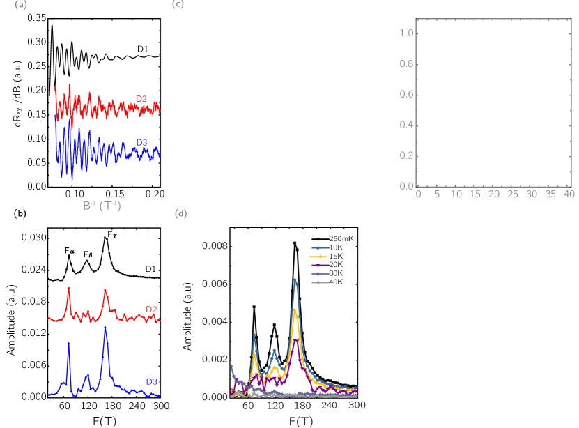
More information can be gained by analyzing the SdH conductance oscillations present in all our devices, visible in both the and curves (see the inset of Fig. 2d). To facilitate their analysis we look at the derivative of and , shown in Fig. 2e and Fig. 3a. An estimate of the charge carrier mobility is obtained from the magnetic field at which the oscillations start, using the criterion ; T depending on the specific device implies mobility values in the range . The values correspond to the electron mobility, as the sign of the Hall slope indicates that it is the electrons that give the dominant contribution to transport.
When plotted against the oscillations exhibit an irregular envelope (Fig. 3a), originating from the presence of multiple frequencies. Indeed, three peaks are present in the amplitude of the Fourier transform (FT), shown in Fig. 3b, centered at frequencies T, T and T. The frequencies coincide in the three different devices (albeit the amplitude of the peak at nearly vanishes in device D2), indicating that the areas of the extremal Fermi surfaces responsible for the SdH oscillations are the same in all cases. It directly follows that –within the material band structure– the Fermi level is located at the same energy in the different devices, and therefore that also the charge carrier density is the same. This confirms our interpretation of the Hall data, namely that the sample-to-sample dependence of the Hall slope is due to variations in the ratio, with that is approximately two times smaller than . Note that with such values the onset of hole SdH oscillations is expected to occur at approximately T in the best devices, so that quantum oscillations of holes are not visible in our experiments.
The evolution of the SdH oscillations upon increasing temperature (see Fig. 3(c) for data measured on device D1) is of particular interest as it allows the cyclotron mass to be determined. The analysis of the data relies on the Lifshitz-Kosevich expression for the and dependence of the oscillation amplitude Schoenberg ; LK ; Richards1973 ; Niederer1974 ; Fang1977 :
| (1) |
where and is the Boltzmann constant, is the temperature. The presence of multiple SdH oscillation frequencies, however, makes the situation complex. That is why we start by discussing in detail how the LK expression can be used in the present context to extract reliable quantitative information.
The common way to extract the cyclotron mass from SdH oscillations consists in plotting a resistance minimum measured at a fixed value of as a function of , and subsequently fitting the data to the dependence predicted by Eq. (1) . This procedure works well in the presence of a single oscillation frequency, but it does not work if multiple frequencies are present. Without going into the microscopic physical details, that is because in the presence of multiple frequencies, the magnetic field values at which the SdH oscillation minima occur are found to vary upon changing (contrary to the case in which a single SdH oscillation frequency is present). Hence, it is simply not possible to analyze the resistance minima at a fixed value of as a function of .
The issue is well-known from past work on materials exhibiting SdH oscillations with multiple frequenciesBalicas2000 ; Bangura2008 ; Cai2015 ; Rhodes2015 . In those systems, a commonly employed heuristic approach to analyze the temperature dependence of SdH oscillations consists in plotting the amplitude of a FT peak as a function of and fitting it with the expression , i.e., with the same functional dependence normally used to fit the -dependence of the resistivity minima. Although believed to give reasonable estimates for the cyclotron masses, this approach is problematic because the temperature dependence of the FT peak, as calculated from the LK expression, is not proportional to . A simple way to understand the problem is to realize that –since – fitting the temperature dependence with the expression requires a specific value of magnetic field to be selected. The FT peak amplitude, however, is calculated by integrating the SdH oscillations over a large interval of magnetic field and not at one specific value of . Therefore, the choice for the value of to be inserted in is arbitrary, which prevents a truly reliable determination of .
We adopt a different approach, free from any ambiguity, that eliminates these problems. It consists in calculating the FT of the LK expression (Eq. (1)) and comparing the -dependence of the calculated FT peak amplitude to the -dependence of the corresponding experimentally measured quantity, using the cyclotron mass as a fitting parameter. The approach is free from ambiguity, because it compares the same quantity, measured or calculated.
Fig. 3d shows the FT of the SdH oscillations measured on device D1 for different values of , ranging from 250 mK to 40 K. The colored dots in Fig. 3e represent the heights of the three FT peaks (normalized to the height at the lowest temperature of our experiments, i.e. 250 mK), extracted from the data in Fig. 3d. The continuous lines of the corresponding color are best fits obtained by using the FT of the LK formula, calculated in the same -range used to calculate the FT of the experimental data 111The experimental spectra used in the analyses are obtained by calculating the FT of the the derivative of the SdH oscillations, for consistency we use the FT spectra of the derivative of equation (1). For each peak, the only fitting parameter is the cyclotron mass, as for all three peaks the carrier mobility (that also enters the theoretical expression) is fixed to be the value determined by the onset of the SdH oscillations. The agreement between data and the curves calculated from the LK expression is excellent and the value of the cyclotron mass extracted for each peak is given in Table 1 (for the peak corresponding to the frequency , the quality of the data only allows us to determine the mass for device D1).
| Device | |||
|---|---|---|---|
| D1 | 0.110 | 0.135 | 0.130 |
| D2 | 0.110 | - | 0.127 |
| D3 | 0.103 | - | 0.125 |
The procedure can be applied not only to the analysis of the -dependence of the peak height, but also to the full functional dependence of the peaks, i.e. to their line-shape. This is useful because at sufficiently low temperature, the peak width is determined by the carrier mobility, and the comparison between calculated and measured FT can enable a more precise determination of this quantity. We illustrate the concept for device D1, for which the blue curve in Fig. 3f is calculated assuming , and for the mobility values of the electrons in the pockets responsible for the different peaks in the FT. It is apparent that with these values the agreement with the data at high frequency is improved. Although a precise optimization is not particularly relevant in the present case, it is important to realize that using the LK formula properly to analyze the FT of the SdH oscillations offers possibilities that go beyond the heuristic approach that is commonly employed.
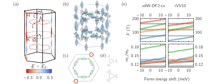
The information about the extremal Fermi surfaces extracted from the analysis of the SdH oscillations are largely consistent with the properties of the electron pockets of bulk jacutingaite computed by density-functional theory (DFT; simulations were done using the Quantum ESPRESSO distributiongiannozzi_quantum_2009 ; giannozzi_qe_2017 ; see SI for details). When SOI is neglected (see Fig. 1b), a degeneracy between the top valence and bottom conduction bands is enforced along the vertical edges of the Brillouin zone by the 3-fold rotation symmetry of the crystal (see the KH line in Fig. 1b), and gives rise to nodal lines. Additional crossings between valence and conduction bands occur away from high-symmetry directions as a consequence of a band inversion driven by the strong interlayer couplingtheory_jacu_2019 (see the line in Fig. 1b), forming two additional nodal loopsbansil_arxiv_2019 ; theory_jacu_2019 . The location within the Brillouin zone of these nodal lines and nodal loops is reported in Fig. 4a. The color coding denotes the common energy of the valence and conduction bands along the nodes relative to the Fermi level (blue = above; red = below), with the dispersion resulting in multiple hole and electron pockets.
To enable comparison with experiments we perform additional DFT simulations including SOI effects. The nodal lines and loops become slightly gapped, but the overall qualitative picture does not change. Fig. 4b shows the corresponding Fermi surface, where electron and hole pockets are represented in blue and grey respectively, in good agreement (in terms of number and polarity) with the expectations from Fig. 4a. We identify four symmetry-inequivalent electron pockets and two pockets with hole character. The extremal contours of these pockets orthogonal to the magnetic field direction (-axis) are also reported, with solid (dashed) lines corresponding to positive (negative) values of . Their projection on the plane is shown in Fig. 4c, with the same color coding as in panel b. This projection is in very good agreement with recent ARPES measurementsCucchi2019 , with the only difference that the two types of hole pockets are merged into one in experiments. This qualitative feature is not captured by DFT, unless the Fermi energy is shifted on the hole side by few meVs (see panel d).
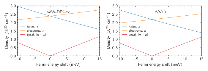
The area of the extremal contours of the Fermi surface that we identity provides an estimate for the expected SdH oscillation frequencies through the Onsager relationOnsager1952 , while the cyclotron mass can be computed through the derivative with respect to the Fermi energySchoenberg . For electron pockets, in Fig. 4e we show the predicted values of and as a function of the shift in Fermi energy with respect to the DFT reference value, obtained for structures relaxed using two different vdW-compliant functionals (the shift in Fermi energy –over a small range, see SI for a quantitative estimate of the corresponding changes in electron/hole densities– is meant to account either for the presence of small doping due to slight deviations from perfect stoichiometry for an unprecise quantitative prediction of the semimetallic band overlap in DFT ). The calculated frequencies corresponding to the four inequivalent electron pockets are in the same range as the experimentally determined values (gray horizontal lines). Similar agreement is found for (for both functionals the calculated cyclotron mass of one pocket –green circles– falls outside the measured range by approximately 30 %). For holes, we find that, when the Fermi energy is shifted so that the hole pockets merge (see Fig. 4d) as seen in ARPES, the overall cyclotron mass becomes very large, on the order of the bare electron mass, resulting in a strong suppression of magnetic oscillations associated with holes. This explains why in the experiments no frequencies corresponding to hole SdH oscillations are detected. We conclude that both functionals show an overall reasonable agreement with the experiments, and correctly capture the magnitude the observed SdH oscillation frequencies and of the corresponding cyclotron masses; deviations are small and concern details beyond what can be expected from this first experimental work on the transport properties of jacutingaite.
IV Conclusion
In summary, the results presented here demonstrate the possibility to realize nano-structured devices based on exfoliated jacutingaite (Pt2HgSe3) crystals that enable the observation of high-quality transport properties. The observed electron mobility values are comparable to those reported in WTe2 layers of the same thickness. This is an extremely promising result, given that our jacutingaite devices are based on crystals grown by using a newly developed process that offers considerable margins of improvement. Crystal growth under high pressure occurs within a short time (hours) and imposes large mechanical constraints to the growing crystals. Fine tuning the growth parameters and making the growth time longer is expected to provide larger crystals of even higher quality, and to allow much larger exfoliated layers to be produced, eventually enabling the realization of monolayer devices. Given that all experiments performed until now –both the transport measurements discussed here and ARPES experiments recently reported– have shown an overall excellent agreement with the predictions of first-principles calculations. We therefore expect that jacutingaite monolayer devices will represent an extremely promising platform to investigate transport in 2D quantum spin Hall insulators, for which the experiments reported here represent and important and necessary first step.
Acknowledgements.
We sincerely acknowledge Alexandre Ferreira for technical support and Antimo Marrazzo for useful discussions. A.F.M. gratefully acknowledges financial support from the Swiss National Science Foundation (Division II) and from the EU Graphene Flagship project. M.G. and M.F. acknowledge support from the Swiss National Science Foundation through the Ambizione program (grants PZ00P2_174056 and PZ00P2_174038). Simulation time was provided by CSCS on Piz Daint (project IDs s825 and s917).References
- (1) C. L. Kane and E. J. Mele, Quantum Spin Hall Effect in Graphene, Physical Review Letters 95, 226801 (2005).
- (2) C. L. Kane and E. J. Mele, Topological Order and the Quantum Spin Hall Effect, Physical Review Letters 95, 146802 (2005).
- (3) B. A. Bernevig and S.-C. Zhang, Quantum Spin Hall Effect, Phys. Rev. Lett. 96, 106802 (2006).
- (4) M. König, S. Wiedmann, C. Brüne, A. Roth, H. Buhmann, L. W. Molenkamp, X.-L. Qi, and S.-C. Zhang, Quantum Spin Hall Insulator State in HgTe Quantum Wells, Science 318, 766 (2007).
- (5) I. Knez, R. R. Du, and G. Sullivan, Evidence for helical edge modes in inverted InAs/GaSb quantum wells, Physical Review Letters 107, 1 (2011).
- (6) K. Suzuki, Y. Harada, K. Onomitsu, and K. Muraki, Edge channel transport in the InAs/GaSb topological insulating phase, Physical Review B - Condensed Matter and Materials Physics 87, 1 (2013).
- (7) Z. Fei, T. Palomaki, S. Wu, W. Zhao, X. Cai, B. Sun, P. Nguyen, J. Finney, X. Xu, and D. H. Cobden, Edge conduction in monolayer , Nature Physics 13, 677 (2017).
- (8) S. Wu, V. Fatemi, Q. D. Gibson, K. Watanabe, T. Taniguchi, R. J. Cava, and P. Jarillo-Herrero, Observation of the quantum spin Hall effect up to 100 kelvin in a monolayer crystal, Science 359, 76 (2018).
- (9) A. Roth, C. Brüne, H. Buhmann, L. W. Molenkamp, J. Maciejko, X.-L. Qi, and S.-C. Zhang, Nonlocal Transport in the Quantum Spin Hall State, Science 325, 294 (2009).
- (10) G. Grabecki, J. Wróbel, M. Czapkiewicz, L. Cywiński, S. Gierałtowska, E. Guziewicz, M. Zholudev, V. Gavrilenko, N. N. Mikhailov, S. A. Dvoretski, F. Teppe, W. Knap, and T. Dietl, Nonlocal resistance and its fluctuations in microstructures of band-inverted HgTe/(Hg,Cd)Te quantum wells, Phys. Rev. B 88, 165309 (2013).
- (11) M. König, M. Baenninger, A. G. F. Garcia, N. Harjee, B. L. Pruitt, C. Ames, P. Leubner, C. Brüne, H. Buhmann, L. W. Molenkamp, and D. Goldhaber-Gordon, Spatially Resolved Study of Backscattering in the Quantum Spin Hall State, Phys. Rev. X 3, 021003 (2013).
- (12) C. Wu, B. A. Bernevig, and S.-C. Zhang, Helical Liquid and the Edge of Quantum Spin Hall Systems, Phys. Rev. Lett. 96, 106401 (2006).
- (13) T. L. Schmidt, Current Correlations in Quantum Spin Hall Insulators, Phys. Rev. Lett. 107, 096602 (2011).
- (14) J. C. Budich, F. Dolcini, P. Recher, and B. Trauzettel, Phonon-Induced Backscattering in Helical Edge States, Phys. Rev. Lett. 108, 086602 (2012).
- (15) J. I. Väyrynen, M. Goldstein, and L. I. Glazman, Helical Edge Resistance Introduced by Charge Puddles, Phys. Rev. Lett. 110, 216402 (2013).
- (16) J. Wang, Y. Meir, and Y. Gefen, Spontaneous Breakdown of Topological Protection in Two Dimensions, Phys. Rev. Lett. 118, 046801 (2017).
- (17) P. Novelli, F. Taddei, A. K. Geim, and M. Polini, Failure of Conductance Quantization in Two-Dimensional Topological Insulators due to Nonmagnetic Impurities, Phys. Rev. Lett. 122, 016601 (2019).
- (18) X. Qian, J. Liu, L. Fu, and J. Li, Quantum spin Hall effect in two- dimensional transition metal dichalcogenides, Science express 10, 1126 (2014).
- (19) S. Tang, C. Zhang, D. Wong, Z. Pedramrazi, H. Z. Tsai, C. Jia, B. Moritz, M. Claassen, H. Ryu, S. Kahn, J. Jiang, H. Yan, M. Hashimoto, D. Lu, R. G. Moore, C. C. Hwang, C. Hwang, Z. Hussain, Y. Chen, M. M. Ugeda, Z. Liu, X. Xie, T. P. Devereaux, M. F. Crommie, S. K. Mo, and Z. X. Shen, Quantum spin Hall state in monolayer , Nature Physics 13, 683 (2017).
- (20) Y. Shi, J. Kahn, B. Niu, Z. Fei, B. Sun, X. Cai, B. A. Francisco, D. Wu, Z. X. Shen, X. Xu, D. H. Cobden, and Y. T. Cui, Imaging quantum spin Hall edges in monolayer , Science Advances 5, 1 (2019).
- (21) I. Cucchi, I. Gutiérrez-Lezama, E. Cappelli, S. M. K. Walker, F. Y. Bruno, G. Tenasini, L. Wang, N. Ubrig, C. Barreteau, E. Giannini, M. Gibertini, A. Tamai, A. F. Morpurgo, and F. Baumberger, Microfocus Laser-Angle-Resolved Photoemission on Encapsulated Mono-, Bi-, and Few-Layer , Nano Letters 19, 554 (2019).
- (22) F. Zheng, C. Cai, S. Ge, X. Zhang, X. Liu, H. Lu, Y. Zhang, J. Qiu, T. Taniguchi, K. Watanabe, S. Jia, J. Qi, J.-H. Chen, D. Sun, and J. Feng, On the Quantum Spin Hall Gap of Monolayer , Advanced Materials 28, 4845 (2016).
- (23) X. Li, Z. Zhang, Y. Yao, and H. Zhang, High Throughput Screening for Two-Dimensional Topological Insulators, 2D Materials 5, 045023 (2018).
- (24) T. Olsen, E. Andersen, T. Okugawa, D. Torelli, T. Deilmann, and K. S. Thygesen, Discovering Two-Dimensional Topological Insulators from High-Throughput Computations, Physical Review Materials 3, 024005 (2019).
- (25) A. Marrazzo, M. Gibertini, D. Campi, N. Mounet, and N. Marzari, Abundance of topological order in exfoliable two-dimensional insulators, arXiv:1908.08334 (2019).
- (26) A. Marrazzo, M. Gibertini, D. Campi, N. Mounet, and N. Marzari, Prediction of a Large-Gap and Switchable Kane-Mele Quantum Spin Hall Insulator, Phys. Rev. Lett. 120, 117701 (2018).
- (27) J. I. Facio, S. K. Das, Y. Zhang, K. Koepernik, J. van den Brink, and I. C. Fulga, Dual topology in jacutingaite , Phys. Rev. Materials 3, 074202 (2019).
- (28) B. Ghosh, S. Mardanya, B. Singh, X. Zhou, B. Wang, T.-R. Chang, C. Su, H. Lin, A. Agarwal, and A. Bansil, Saddle-point von Hove singularity and dual topological insulator state in Pt2HgSe3, arXiv:1905.12578 (2019).
- (29) A. Marrazzo, N. Marzari, and M. Gibertini, Emergent dual topology in the three-dimensional Kane-Mele , arXiv:1909.05050 (2019).
- (30) I. Cucchi, A. Marrazzo, E. Cappelli, S. Ricco, F. Y. Bruno, S. Lisi, M. Hoesch, T. K. Kim, C. Cacho, C. Besnard, E. Giannini, N. Marzari, M. Gibertini, F. Baumberger, and A. Tamai, Bulk and surface electronic structure of the dual-topology semimetal , arXiv:1909.05051 (2019).
- (31) K. Kandrai, G. Kukucska, P. Vancsó, J. Koltai, G. Baranka, Z. E. Horváth, Á. Hoffmann, A. Vymazalová, L. Tapasztó, and P. Nemes-Incze, Evidence for room temperature quantum spin Hall state in the layered mineral jacutingaite, arXiv:1903.02458 (2019).
- (32) X. Wu, M. Fink, W. Hanke, R. Thomale, and D. Di Sante, Unconventional superconductivity in a doped quantum spin Hall insulator, Phys. Rev. B 100, 041117(R) (2019).
- (33) A. R. Cabral, H. F. Galbiatti, R. Kwitko-Ribeiro, and B. Lehmann, Platinum Enrichment at Low Temperatures and Related Microstructures, with Examples of Hongshiite (PtCu) and Empirical ‘’ from Itabira, Minas Gerais, Brazil, Terra Nova 20, 32 (2008).
- (34) L. Wang, I. Gutiérrez-Lezama, C. Barreteau, N. Ubrig, E. Giannini, and A. F. Morpurgo, Tuning magnetotransport in a compensated semimetal at the atomic scale, Nature Communications 6, 1 (2015).
- (35) L. Wang, I. Gutiérrez-Lezama, C. Barreteau, D.-K. Ki, E. Giannini, and A. F. Morpurgo, Direct Observation of a Long-Range Field Effect from Gate Tuning of Nonlocal Conductivity, Phys. Rev. Lett. 117, 176601 (2016).
- (36) A. Vymazalová, F. Laufek, M. Drábek, A. R. Cabral, J. Haloda, T. Sidorinová, B. Lehmann, H. F. Galbiatti, and J. Drahokoupil, Jacutingaite, , a new platinum-group mineral species from the Cauê iron-ore deposit, Itabira district, Minas Gerais, Brazil, The Canadian Mineralogist 50, 431 (2012).
- (37) M. O’Brien, N. McEvoy, C. Motta, J.-Y. Zheng, N. C. Berner, J. Kotakoski, K. Elibol, T. J. Pennycook, J. C. Meyer, C. Yim, M. Abid, T. Hallam, J. F. Donegan, S. Sanvito, and G. S. Duesberg, Raman characterization of platinum diselenide thin films, 2D Materials 3, 021004 (2016).
- (38) G. Xu, H. Weng, Z. Wang, X. Dai, and Z. Fang, Chern semimetal and the quantized anomalous Hall effect in HgCr 2 Se 4, Physical Review Letters 107, 1 (2011).
- (39) T. Liang, Q. Gibson, M. N. Ali, M. Liu, R. J. Cava, and N. P. Ong, Ultrahigh mobility and giant magnetoresistance in the Dirac semimetal Cd3As2, Nature Materials 14, 280 (2015).
- (40) C. Shekhar, A. K. Nayak, Y. Sun, M. Schmidt, M. Nicklas, I. Leermakers, U. Zeitler, Y. Skourski, J. Wosnitza, Z. Liu, Y. Chen, W. Schnelle, H. Borrmann, Y. Grin, C. Felser, and B. Yan, Extremely large magnetoresistance and ultrahigh mobility in the topological Weyl semimetal candidate NbP, Nature Physics 11, 645 (2015).
- (41) I. A. Leahy, Y.-P. Lin, P. E. Siegfried, A. C. Treglia, J. C. W. Song, R. M. Nandkishore, and M. Lee, Nonsaturating large magnetoresistance in semimetals, Proceedings of the National Academy of Sciences 115, 10570 (2018).
- (42) J. Ziman, Principles of the Theory of Solids (Cambridge University Press, 1972) ISBN 9780521297332.
- (43) D. Schoenberg, Magnetic Oscillations in Metals (Cambridge University Press, Cambridge, 2009).
- (44) I. Lifshitz and A. Kosevich, Theory of Magnetic Susceptibility in Metals at Low Temperature, Sov. Phys. JETP 2, 636 (1956).
- (45) F. E. Richards, Investigation of the magnetoresistance quantum oscillations in magnesium, Physical Review B 8, 2552 (1973).
- (46) H. H. Niederer, Magneto oscillatory conductance in n-type inverted silicon surfaces, Japanese Journal of Applied Physics 13, 339 (1974).
- (47) F. F. Fang, A. B. Fowler, and A. Hartstein, Effective mass and collision time of (100) Si surface electrons, Phys. Rev. B 16, 4446 (1977).
- (48) L. Balicas, J. S. Brooks, K. Storr, D. Graf, S. Uji, H. Shinagawa, E. Ojima, H. Fujiwara, H. Kobayashi, A. Kobayashi, and M. Tokumoto, Shubnikov-de Haas effect and Yamaji oscillations in the antiferromagnetically ordered organic superconductor -(BETS)2FeBr4: A fermiology study, Solid State Communications 116, 557 (2000).
- (49) A. F. Bangura, J. D. Fletcher, A. Carrington, J. Levallois, M. Nardone, B. Vignolle, P. J. Heard, N. Doiron-Leyraud, D. Leboeuf, L. Taillefer, S. Adachi, C. Proust, and N. E. Hussey, Small fermi surface pockets in underdoped high temperature superconductors: Observation of Shubnikov-de Haas oscillations in YBa2Cu4O8, Physical Review Letters 100, 1 (2008).
- (50) P. L. Cai, J. Hu, L. P. He, J. Pan, X. C. Hong, Z. Zhang, J. Zhang, J. Wei, Z. Q. Mao, and S. Y. Li, Drastic Pressure Effect on the Extremely Large Magnetoresistance in WTe2: Quantum Oscillation Study, Physical Review Letters 115, 1 (2015).
- (51) D. Rhodes, S. Das, Q. R. Zhang, B. Zeng, N. R. Pradhan, N. Kikugawa, E. Manousakis, and L. Balicas, Role of spin-orbit coupling and evolution of the electronic structure of WTe2 under an external magnetic field, Physical Review B - Condensed Matter and Materials Physics 92, 1 (2015).
- (52) The experimental spectra used in the analyses are obtained by calculating the FT of the the derivative of the SdH oscillations, for consistency we use the FT spectra of the derivative of equation (1\@@italiccorr)
- (53) M. Dion, H. Rydberg, E. Schröder, D. C. Langreth, and B. I. Lundqvist, Van der Waals Density Functional for General Geometries, Phys. Rev. Lett. 92, 246401 (2004).
- (54) K. Berland and P. Hyldgaard, Exchange functional that tests the robustness of the plasmon description of the van der Waals density functional, Phys. Rev. B 89, 035412 (2014).
- (55) O. A. Vydrov and T. Van Voorhis, Nonlocal van der Waals density functional: The simpler the better, The Journal of Chemical Physics 133, 244103 (2010).
- (56) R. Sabatini, T. Gorni, and S. de Gironcoli, Nonlocal van der Waals density functional made simple and efficient, Phys. Rev. B 87, 041108 (2013).
- (57) P. Giannozzi, S. Baroni, N. Bonini, M. Calandra, R. Car, C. Cavazzoni, Davide Ceresoli, G. L. Chiarotti, M. Cococcioni, I. Dabo, A. D. Corso, S. de Gironcoli, S. Fabris, G. Fratesi, R. Gebauer, U. Gerstmann, C. Gougoussis, Anton Kokalj, M. Lazzeri, L. Martin-Samos, N. Marzari, F. Mauri, R. Mazzarello, Stefano Paolini, A. Pasquarello, L. Paulatto, C. Sbraccia, S. Scandolo, G. Sclauzero, A. P. Seitsonen, A. Smogunov, P. Umari, and R. M. Wentzcovitch, QUANTUM ESPRESSO: A Modular and Open-Source Software Project for Quantum Simulations of Materials, Journal of Physics: Condensed Matter 21, 395502 (2009).
- (58) P. Giannozzi, O. Andreussi, T. Brumme, O. Bunau, M. B. Nardelli, M. Calandra, R. Car, C. Cavazzoni, D Ceresoli, M. Cococcioni, N. Colonna, I. Carnimeo, A. D. Corso, S. de Gironcoli, P. Delugas, R. A. D. Jr, A Ferretti, A. Floris, G. Fratesi, G. Fugallo, R. Gebauer, U. Gerstmann, F. Giustino, T. Gorni, J. Jia, M. Kawamura, H-Y Ko, A. Kokalj, E. Küçükbenli, M. Lazzeri, M. Marsili, N. Marzari, F. Mauri, N. L. Nguyen, H.-V. Nguyen, A Otero-de-la-Roza, L. Paulatto, S. Poncé, D. Rocca, R. Sabatini, B. Santra, M. Schlipf, A. P. Seitsonen, A. Smogunov, I Timrov, T. Thonhauser, P. Umari, N. Vast, X. Wu, and S. Baroni, Advanced Capabilities for Materials Modelling with Q Uantum ESPRESSO, Journal of Physics: Condensed Matter 29, 465901 (2017).
- (59) L. Onsager, Interpretation of the de Haas-van Alphen effect, Phil. Mag. 43, 1006 (1952).
- (60) M. Drábek, A. Vymazalová, and A. R. Cabral, The system Hg-Pt-Se At 400C: Phase relations involving jacutingaite, Canadian Mineralogist 50, 441 (2012).
- (61) G. Prandini, A. Marrazzo, I. E. Castelli, N. Mounet, and N. Marzari, Precision and efficiency in solid-state pseudopotential calculations, npj Computational Materials 4, 72 (2018).
- (62) M. J. van Setten, M. Giantomassi, E. Bousquet, M. J. Verstraete, D. R. Hamann, X. Gonze, and G. M. Rignanese, The PseudoDojo: Training and grading a 85 element optimized norm-conserving pseudopotential table, Computer Physics Communications 226, 39 (2018).
- (63) N. Marzari, D. Vanderbilt, A. De Vita, and M. C. Payne, Thermal Contraction and Disordering of the Al(110) Surface, Phys. Rev. Lett. 82, 3296 (1999).
- (64) N. Marzari, A. A. Mostofi, J. R. Yates, I. Souza, and D. Vanderbilt, Maximally Localized Wannier Functions: Theory and Applications, Reviews of Modern Physics 84, 1419 (2012).
- (65) A. A. Mostofi, J. R. Yates, G. Pizzi, Y.-S. Lee, I. Souza, D. Vanderbilt, and N. Marzari, An Updated Version of Wannier90: A Tool for Obtaining Maximally-Localised Wannier Functions, Computer Physics Communications 185, 2309 (2014).
- (66) P. Rourke and S. Julian, Numerical extraction of de Haas–van Alphen frequencies from calculated band energies, Computer Physics Communications 183, 324 (2012).
- (67) Q. Wu, S. Zhang, H.-F. Song, M. Troyer, and A. A. Soluyanov, WannierTools: An open-source software package for novel topological materials, Computer Physics Communications 224, 405 (2018).
- (68) K. Lee, E. D. Murray, L. Kong, B. I. Lundqvist, and D. C. Langreth, Higher-accuracy van der Waals density functional, Phys. Rev. B 82, 081101 (2010).
- (69) A. Togo and I. Tanaka, First principles phonon calculations in materials science, Scr. Mater. 108, 1 (2015).
- (70) V. R. Cooper, Van der Waals density functional: An appropriate exchange functional, Phys. Rev. B 81, 161104 (2010).
- (71) J. c. v. Klimeš, D. R. Bowler, and A. Michaelides, Van der Waals density functionals applied to solids, Phys. Rev. B 83, 195131 (2011).
- (72) J. Klimeš, D. R. Bowler, and A. Michaelides, Chemical accuracy for the van der Waals density functional, Journal of Physics: Condensed Matter 22, 022201 (2009).
Supporting Information
S1 Details on crystal growth
Because of the high vapour pressure of mercury at low temperatures and the high reaction temperature needed for alloying platinum, the growth of must be carried out under extreme conditions. Single crystals of jacutingaite have been grown from the melt under high isostatic pressure in a hot-stage cubic-anvil press. The precursor components Pt (sponge, 99.98%), (powder, 99.9%) and Se (shot, 99.999%) have been mixed with a nominal slightly Hg-exceeding composition inside a Ar-filled glove box, and pelletized to a relative mass density of . The pellet was tightly inserted into a BN crucible, covered by BN caps, and placed inside a cylinder-like graphite heater. The heater fits inside a pyrophillite cubic cell, the pressure transmitter, on each face of which a WC piston acts, thus transforming a uni-axial force in a quasi-isostatic pressure on the sample. With this apparatus, we could process the material at temperatures of 800-1000 ∘C under a pressure of 1-2 GPa. After quite a short heating and cooling process (1-2h at the maximum temperature followed by cooling at 50-70 ∘C/h down to 650∘C), crystals of have grown inside the pellet and could be mechanically extracted.
The largest size of the crystals was in the cleavage plane (perpendicular to the crystallographic c-axis). Owing to the very high density of the as-grown polycrystalline bulk, the crystal size is limited and the extraction of the crystal is a delicate operation. However, the use of high pressure strongly improves the growth kinetics and allows obtaining bulk crystals within few hours, while the vapor-solid reaction technique reportedjacutingaite_exp_12 could only produce powder samples over a time scale of 70 days.
Single crystals were mechanically extracted from the as-grown boule and individually checked for structural and chemical quality, by means of X-ray diffraction (XRD) and Wavelength Dispersive X-ray Spectroscopy (WDS). The single-crystal XRD confirmed the crystal structure previously reported for jacutingaite jacutingaite_exp_12 . WDS chemical analysis was performed with a Oxford Aztec Advance complete WDS system coupled to a SDD detector X-MaxN80, installed in a JEOL JSM 7600 F scanning electron microscope. Factory-provided standards Pt, Se and HgTe were used for quantitative calibration. The Pt:Hg ratio was found to be equal to , averaging over various crystals, thus confirming that no Hg vacancies are present in these crystals at an appreciable amount. Accordingly, the Hg-site in the crystal structure is found to be fully occupied by the Rietveld profile refinement of powder XRD diffraction patterns.
Part of the as-grown pellet was ground and used for powder X-ray diffraction. Reflections from the secondary phase were often present in the powder diffraction pattern (up to 6-7% in volume) and rare single crystals of were found as well, with a similar size and aspect to those of . In fact, can stably form in the same temperature range as and, because of its structural similarity, can even grow epitaxially next to a grain, as already reportedDrabek2012 . For this reason, it was mandatory to analyze carefully every single crystal prior to proceeding with device preparation and physical measurements.
S2 Details of first-principles calculations
First-principles simulations have been carried out within density-functional theory using the Quantum ESPRESSO distribution giannozzi_quantum_2009 ; giannozzi_qe_2017 . Several van-der-Waals compliant functionals have been adopted to relax the atomic positions until the residual force on each atoms was smaller than 2.5 mev/Å, while keeping the unit cell fixed to the experimental one. At this stage spin-orbit coupling has been neglected and electron-ion interactions have been approximated using pseudopotentials from the Standard Solid State pseudopotential libraryprandini_precision_2018 (v1.0), with a cutoff of 50 Ry on energy and 280 Ry on the charge density. Spin-orbit coupling is then included in calculations on the relaxed structure by using fully relativistic pseudopotentials from the Pseudo-Dojo librarydojo_paper_18 with a energy cutoff of 80 Ry. The Brillouin zone is sampled using a -centered Monkhorst-Pack grid with a cold smearingmv_smearing_99 of 0.015 Ry. To compute the Fermi surface, energy bands are interpolated by mapping the electronic states onto a set of maximally-localized Wannier functionswannier_review_12 using WANNIER90mostofi_updated_2014 . As starting projections we consider - and -orbitals on Hg and Pt, together with -orbitals on Se, and the wannierization is performed on a regular grid over the Brillouin zone. The Fermi surface is computed from energy bands Wannier interpolated over a dense k-grid. The SKEAF softwareRourke2012 is then adopted to extract the extremal contours, their areas, and the corresponding cyclotron mass. Wannier functions are used also to obtain the reciprocal space dispersion of the nodal loops with the help of the WannierTools softwarewannier_tools_18 .
S3 Computed frequencies of Raman active modes
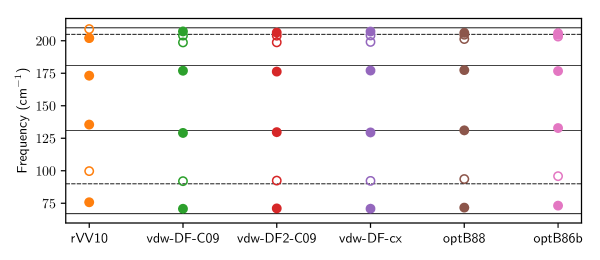
| rVV10 Vydrov2010 ; Sabatini2013 | vdw-DF-c09 Dion2004 ; Cooper2010 | vdw-DF2-c09 Lee2010 ; Cooper2010 | vdw-DF-cx Berland2014 | optB86b Klimes2011 | optB88 Klimes2009 | ||||||
|---|---|---|---|---|---|---|---|---|---|---|---|
| 65.8 | Eu | 62.6 | Eu | 62.8 | Eu | 62.7 | Eu | 63.5 | Eu | 64.8 | Eu |
| 75.8 | Eg | 70.8 | Eg | 71.1 | Eg | 70.8 | Eg | 71.7 | Eg | 73.2 | Eg |
| 91.2 | A1u | 86.3 | A2u | 86.6 | A2u | 86.6 | A2u | 88.0 | A2u | 89.9 | A2u |
| 91.4 | A2u | 92.0 | A1u | 91.6 | A1u | 91.9 | A2u | 92.0 | A1u | 92.4 | A1u |
| 93.4 | A2u | 92.0 | A1g | 91.8 | A2u | 91.9 | A1u | 92.3 | A2u | 93.4 | A2u |
| 93.7 | Eu | 92.0 | A2u | 91.9 | Eu | 92.2 | Eu | 93.0 | Eu | 94.0 | Eu |
| 99.8 | A1g | 92.1 | Eu | 92.5 | A1g | 92.2 | A1g | 93.7 | A1g | 95.9 | A1g |
| 118.7 | Eu | 115.8 | Eu | 115.8 | Eu | 115.8 | Eu | 116.3 | Eu | 117.3 | Eu |
| 135.6 | Eg | 129.1 | Eg | 129.7 | Eg | 129.5 | Eg | 131.1 | Eg | 132.9 | Eg |
| 140.4 | Eu | 140.0 | Eu | 139.9 | Eu | 140.1 | Eu | 140.4 | Eu | 140.7 | Eu |
| 152.1 | A2u | 146.6 | A2u | 146.7 | A2u | 146.6 | A2u | 147.5 | A2u | 149.3 | A2u |
| 173.2 | Eg | 177.0 | Eg | 176.3 | Eg | 177.1 | Eg | 177.4 | Eg | 176.7 | Eg |
| 176.5 | A2g | 184.1 | A2g | 183.1 | A2g | 184.0 | A2g | 182.6 | A2g | 180.4 | A2g |
| 201.0 | Eu | 196.5 | Eu | 196.8 | Eu | 196.9 | Eu | 198.3 | Eu | 200.0 | Eu |
| 202.1 | Eg | 198.7 | A1g | 198.8 | A1g | 199.1 | A1g | 201.4 | A1g | 203.2 | A1g |
| 202.2 | A1g | 202.7 | A2u | 202.9 | A2u | 202.9 | A2u | 203.9 | A2u | 204.6 | Eg |
| 207.8 | A2u | 204.0 | A1g | 203.9 | A1g | 204.1 | A1g | 204.7 | A1g | 205.1 | A2u |
| 209.0 | A1g | 207.2 | Eg | 206.3 | Eg | 207.1 | Eg | 206.1 | Eg | 205.8 | A1g |
| 214.1 | A2u | 219.6 | A2u | 218.9 | A2u | 219.6 | A2u | 218.9 | A2u | 217.4 | A2u |
| 218.5 | Eu | 221.6 | Eu | 221.1 | Eu | 221.7 | Eu | 221.3 | Eu | 220.2 | Eu |
| 220.2 | Eu | 225.3 | Eu | 224.5 | Eu | 225.2 | Eu | 224.0 | Eu | 222.1 | Eu |
| 225.9 | A1u | 230.3 | A1u | 229.6 | A1u | 230.3 | A1u | 229.3 | A1u | 227.8 | A1u |
S4 Carrier density evolution with Fermi energy shift