Performance evaluation of a silicon strip detector for positrons/electrons from a pulsed a muon beam
Abstract
A high-intensity pulsed muon beam is becoming available at the at the Japan Proton Accelerator Research Complex (J-PARC). Many experiments to study fundamental physics using this high-intensity muon beam are proposed. An experiment to measure the muon magnetic moment anomaly () and the muon electric dipole moment (EDM) is one of these experiments and it requires a tracking detector for positrons from muon decay. Fine segmentation is required in a detector to tolerate the high rate of positrons. The time resolution is required to be much better than the muon anomalous spin precession period while a buffer depth of a front-end electronics needs to be much longer than the accelerated muon lifetime. Requirements of this detector also meet requirements of a measurement of the muonium hyperfine structure interval at the J-PARC and another experiment to measure the proton charge radius at Tohoku University. We have developed a single-sided silicon strip sensor with a 190 m pitch, a front-end electronics with a sampling rate of 200 MHz and a buffer memory depth of 8192, and a data acquisition system based on DAQ-Middleware for the J-PARC muon /EDM experiment. We have fabricated detector modules consisting of this sensor and the front-end electronics. Performance of fabricated detector modules was evaluated at a laboratory and a beam test using the positron beam at Tohoku University. The detector is confirmed to satisfy all requirements of the experiments except for the time walk, which will be solved by the next version of a front-end electronics.
1 Introduction
1.1 Muon research at J-PARC
A high-intensity pulsed muon beam at the order of muons/s on average is becoming available at the Muon Science Establishment (MUSE) located at the Material and Life Science Experimental Facility (MLF) in the Japan Proton Accelerator Research Complex (J-PARC) [1]. The repetition rate of the beam is 25 Hz. The beam spill consists of two bunches separated by 600 ns with a bunch of 100-150 ns full width. The average intensity will be of the order of muons/s when the 3 GeV proton synchrotron ring of the J-PARC is fully operated and the proton beam power of 1 MW is reached as designed, which is used for generating a muon beam. Short time operation of the proton beam power of 1 MW was demonstrated in 2019 and it will be provided to beam users soon. In a new muon beam line, the H-line, which is being constructed, another factor of improvement is expected in the muon beam intensity [2]. Several experiments are planned at the H-line assuming the beam intensity of muons/s. A high-intensity muon beam is a key to search for new physics beyond the Standard Model in precise measurements of fundamental parameters of the muon with high statistics and is also useful for material science studies based on muon spin spectroscopy.
1.2 Muon /EDM experiment at J-PARC
A new experiment is proposed to measure the muon magnetic moment anomaly () and the muon electric dipole moment (EDM) at the J-PARC MUSE H-line [3]. The experiment uses a different method from the E821 experiment at Brookhaven National Laboratory [4] or the E989 experiment at Fermilab [5] and aims to measure the muon with a statistical uncertainty of 450 parts per billion and the muon EDM with a sensitivity of cm. In this experiment, a muon beam produced by a primary proton beam is slowed down and thermalized in a material. The thermalized muon beam is accelerated to 300 MeV/ to produce a low-emittance muon beam. This muon beam is injected into a storage ring using a novel 3D spiral injection method. The storage ring is a 3 T magnetic resonance imaging-type solenoid with high field uniformity for the muon storage region with an orbit diameter of 66 cm. A tracking detector is placed inside of the magnet and is required to reconstruct positron tracks from muon decay and to estimate the muon decay time. The anomalous spin precession frequency of muons in this magnetic field is measured by the muon decay time distribution with higher-momentum positrons. The sensitivity to the muon spin becomes maximum when positrons with momenta above 200 MeV/ are counted.
1.3 Other experiments
The MuSEUM experiment is another experiment proposed at the J-PARC MUSE H-line to measure the muonium hyperfine structure interval and the ratio of muon to proton magnetic moments by using the muonium spin resonance method at high magnetic field [6]. The number of positrons from decay of the muon beam after forming a muonium and experiencing a resonant microwave is counted as a function of time in this experiment. A detector with fine segementation and a high sampling rate is required to tolerate positrons from a high-intensity muon beam of muons in one spill.
Requirements for detectors in these experiments meet requirements of another experiment proposed at the Research Center for Electron Photon Science (ELPH), Tohoku University, which will measure the proton charge radius by low-energy electron scattering at the lowest momentum ever achieved (ULQ2 experiment) [7]. In this experiment, electrons in the energy range of 20-60 MeV are scattered at a target, and the momentum and the scattering angle of scattered electrons need to be measured. An electron spectrometer with the momentum resolution of and the scattering angle resolution of 5 mrad is developed. To achieve this resolution, a detector with a position resolution much better than 1 mm is required at a focal plane. The expected rate of electrons at the focal plane is 30 MHz in an area of cm2.
1.4 Requirements for tracking system
A positron tracking detector for the J-PARC muon /EDM experiment is required to be sensitive in a volume with a radius of 290 mm and a height of 400 mm. In this volume, 40 layers of detection planes are required to reconstruct positron tracks with the momentum above 200 MeV/ even in the highest muon decay rate. To cover this volume with a reasonable cost, we choose silicon strip detector technology. The maximum number of positrons from muon decay is expected to be six per 1 ns and the maximum hit rate will reach 150 kHz/mm2. The detector is required to tolerate this hit rate and to measure up to four minimum ionizing particle (MIP) charge to accommodate pile-up of hits. The signal-to-noise ratio greater than 15 is required to reconstruct positron tracks in high efficiency. Since the anomalous spin precession period in the magnetic field of 3 T is about 2.1 s, the time resolution is required to be much better than this period. On the other hand, the data needs to be stored sufficiently longer than this period as well as the lifetime of muon with the momentum of 300 MeV/ (6.6 s). Another requirement comes from the pile-up of detector hits. If there are pile-up hits in the same sensor strip, a sensor signal waveform is distorted and the recorded timing is shifted. Since the rate of pile-up changes during the data taking period due to the lifetime of muon, it will bias the spin precession frequency measurement. This effect can be mitigated by a readout system with a small time walk. To constrain this effect, the time walk is required to be less than 1 ns over a signal range of 0.5-3 MIP charge.
To satisfy these requirements, we have developed a single-sided silicon strip sensor and a front-end readout electronics optimized for the experiment. We have fabricated detector modules consisting of this sensor and the readout electronics controlling their qualities. Performance of fabricated detector modules was evaluated at a laboratory and a beam test using the positron beam at the ELPH, Tohoku University. The design and the performance of the detector modules are presented in this article.
2 Detector system
The detector module consists of a silicon strip sensor and two front-end readout boards.
2.1 Sensor
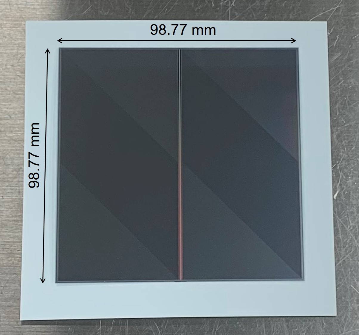
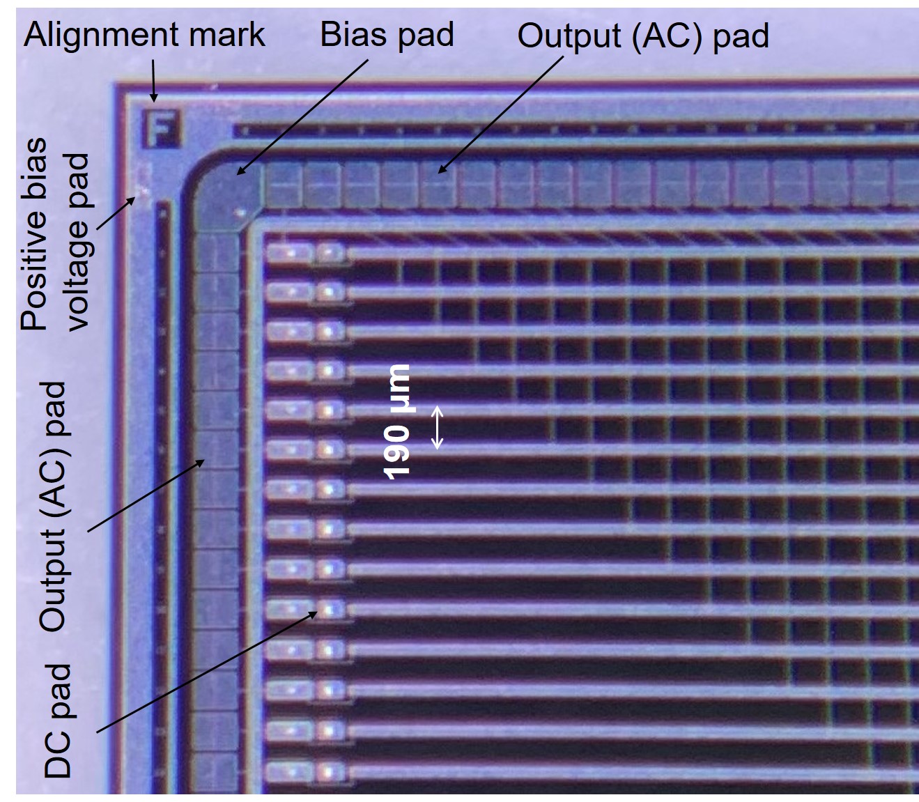
A silicon strip sensor developed for at the J-PARC muon /EDM experiment is used in this module (figure 1). The sensor is a single-sided p-on-n silicon strip sensor with a double-metal structure made by Hamamatsu Photonics K. K. and is now commercially available as a model S13804. The size of the sensor is 98.77 mm 98.77 mm with a thickness of 320 m. The active area is 97.28 mm 97.28 mm. The sensor has two columns of 512 strips with a pitch of 190 m and a length of 48.365 mm. The size of strips is determined to constrain the hit rate less than 2 MHz and the estimated maximum hit rate at the J-PARC muon /EDM experiment with this strip size is 1.4 MHz per strip. Strip sensor signals are read out from AC-coupled output pads. Coupling capacitance between a p+ strip and a read out strip is measured to be 170 pF. Because of double-metal structure, signals can be read out from the orthogonal direction as well. This enables us to use the same design of the readout system for horizontal or vertical strips since the sensor shape is square. By stacking two sensors with different strip directions, two-dimensional coordinates of charged particles passing through two sensors can be determined. To construct 40 detection planes with two-dimentional coordinates for the J-PARC muon /EDM experiment, 640 sensors are used in total.
The p+ strips are connected to a common bias ring via a polysilicon resister of the resistance of M. The bias ring is connected to ground via a bias pad on the surface. The positive bias voltage is applied from either the back plane of the sensor or pads on the surface. The full depletion voltage was measured to be from 65 V to 95 V depending on the sensor according to the measurements by the manufacturer and sensors are usually operated with the bias voltage above 120 V. The capacitance of one strip to the back plane was measured to be about 17 pF above the full depletion voltage. A typical total leakage current of the sensor is about 0.2 A with the bias voltage above the full depletion voltage at room temperature.
2.2 Front-end electronics
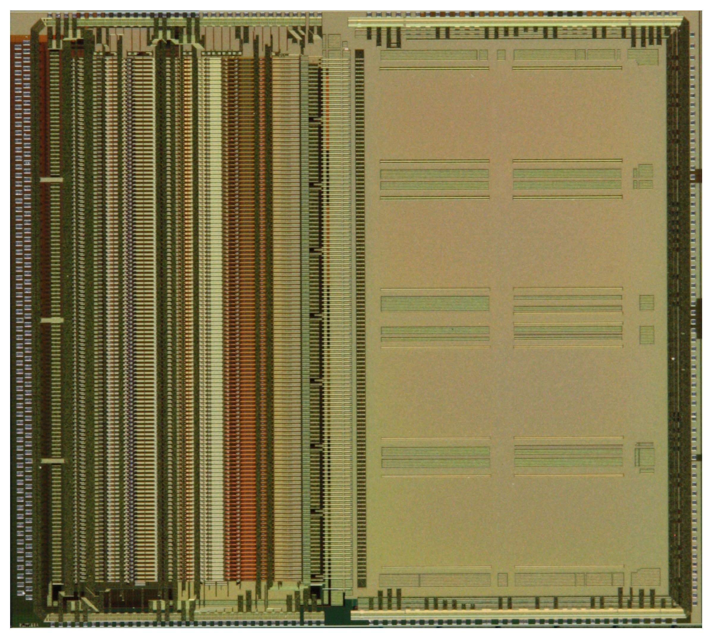
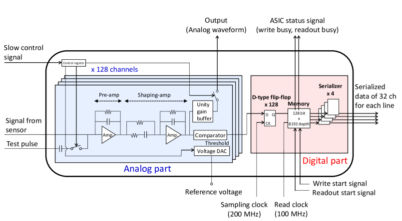
The signals from the silicon strip sensors are read out by front-end boards with application specific integrated circuits (ASICs) named “SliT128A”, which is a prototype of the front-end ASIC for the J-PARC muon /EDM experiment. The SliT128A is implemented in the Silterra 0.18-m CMOS process and has a chip size of 9.0 mm 10.0 mm with 128 readout channels as shown in figure 2. The schematic logic diagram of the SliT128A chips is shown in figure 3. Each channel has an analog part that consists of a preamplifier, a shaping amplifier, and a comparator with a reference voltage set by a 6-bit Digital-to-Analog Converter (DAC). A charge of 3.84 fC (1 MIP) is converted to a signal with a pulse width of about 180 ns by the preamplifier and the shaping amplifier. The threshold value at the comparator is adjustable channel by channel using a 6-bit DAC to compensate for channel-to-channel threshold variations. A monitor line is prepared to examine analog waveforms at the output of the shaping amplifier. The control register enables the test pulse input line and the monitor line and adjusts the threshold DAC.
A digital part consists of 128 D-type flip-flops, a buffer memory and four serializers. The binary signal from the comparator is sampled by the D-type flip-flop with 5 ns intervals provided by an external sampling clock with a frequency of 200 MHz. When the SliT128 chip receives a write start signal, the chip starts to store the sampled data into the memory buffer. For a pulsed (muon) beam, the write start signal is input to the SliT128A chip at the timing of pulsed (muon) beam coming based on a signal from an accelerator. Since the memory buffer has a width of 128 bits and a depth of 8192 points, we can store the data of 128 channels with a period of 40.96 s ( points 5 ns). A readout start signal is input after the end of the writing process is detected by the SliT128A status signal. When the SliT128A chip receives readout start signal, the data stored in the memory buffer is read out through serializers. This readout must be finished before the next beam bunch coming. To shorten read time, four serializers are located and each serializer serializes the data of 32 bits (or channels) times 8192 points based on an external read out clock with a frequency of 100 MHz.
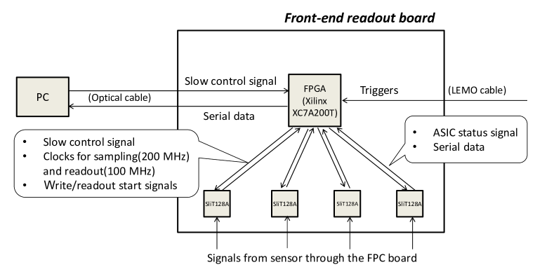
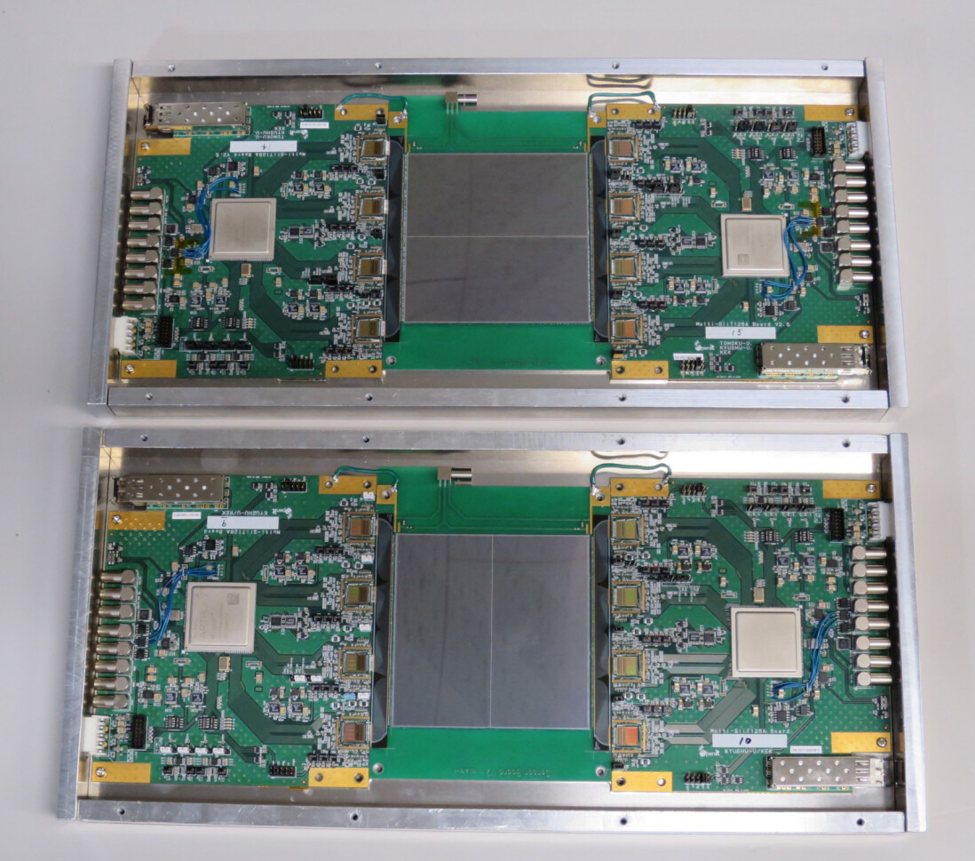
The front-end readout board consists of four SliT128A chips, a Xilinx Artix-7 XC7A200T field-programmable gate array (FPGA), and a small form-factor pluggable (SFP) optical transceiver as shown in figure 4. The data from the SliT128A chips are processed with the FPGA. The start signals for the writing and readout processes can be input to the front-end readout board through the connector with the Nuclear Instrumentation Module (NIM) standard logic. The data from four SliT128A chips are transferred to the first in, first out (FIFO) buffer implemented inside the FPGA simultaneously in parallel, when the start signal for the readout process is asserted. The data of 32 channels with a depth of 8192 points comes per one readout line. The data is saved into the FIFO with a format of 45 bits: 13 bits to represent hit timing and 32 bits to represent existence of hits for each channel. The data can be compressed by the zero suppression algorithm: if all 32 channels have no hits, the data is not stored to the FIFO to suppress the amount of the data. After completing the data transfer from the four SliT128A chips to the FIFO, the data stored in the FIFO is serially transferred to a computer via an optical cable with Ethernet and SiTCP protocols [8].
2.3 Assembly
A sensor is glued on a 1.6 mm-thick glass epoxy circuit board which has a hole in the active area of the sensor. The positive bias voltage is applied from pads on the sensor surface, which is connected to the back plane of the sensor. The bias pads are connected to ground. To suppress parasitic capacitance, the bare SliT128A chips are directly placed on the front-end readout board and are wire bonded using 25 m-diameter aluminum (99% Al with 1% Si) wires. A sensor and SliT128A chips are connected by two flexible printed circuit (FPC) boards. One FPC board connects 512 channels of a sensor to four SliT128A chips. Wire bonding is used to connect a sensor with an FPC board and SliT128A chips with an FPC board.
A glass epoxy circuit board with a sensor and two readout boards are glued on the same 3 mm-thick aluminum plate, which has a hole in the active area of the sensor. Two types of modules were constructed; one with strips in vertical and the other with strips in horizontal direction (figure 5). By stacking two types of modules successively, two-dimensional coordinates of charged particles passing through two modules can be determined.
2.4 Data acquisition system
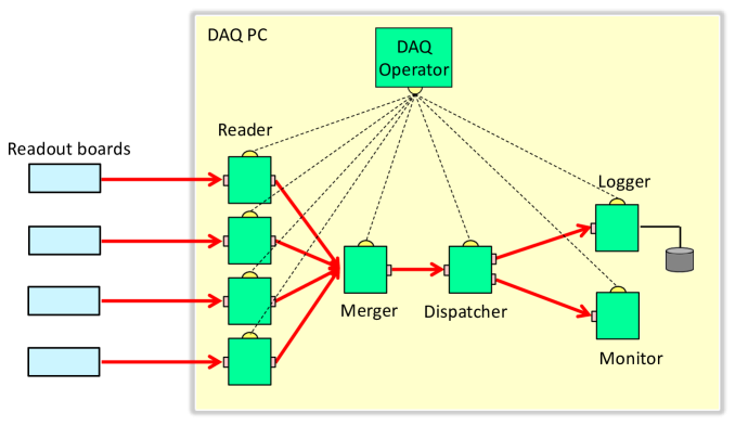
The data acquisition (DAQ) system is constructed based on DAQ-Middleware [9, 10], which is a software framework for network distributed DAQ software. The framework consists of DAQ-Components and a DAQ-Operator. The DAQ-Component is a base unit that can run fully independently of each other. Users can develop a data acquisition path by connecting DAQ-Components. The DAQ-Operator controls DAQ-Components by sending the signals to each DAQ-Component, such as a start and a stop. Figure 6 shows a structure of the DAQ system. There are five types of the DAQ-Components in the DAQ system for this module: reader, merger, dispatcher, logger, and monitor. Data from one front-end readout board is received by a reader component. The data acquisition paths for each front-end readout board are merged by the merger component and the merged path is split into two by the dispatcher component. One path is connected with the storage component and the data is saved in the hard disk drive. The other path is connected with the monitor component and a part of the data is analyzed to monitor the status of the module and the DAQ system itself. The maximum data rate from a front-end readout board is about 20 MB/s without the zero suppression algorithm. It takes about 2.6 ms for the data transfer from four SliT128A chips to the FIFOs in the FPGA and it takes about 5.3 ms per front-end readout board without the zero-suppression algorithm for the data transfer from the FIFOs in the FPGA to a personal computer. One detector module can be operated up to a repetition rate of 75 Hz without the zero-suppression algorithm and it satisfies the requirement of the muon beam rate at the J-PARC.
3 Quality control
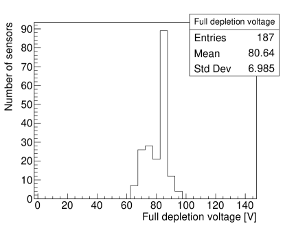
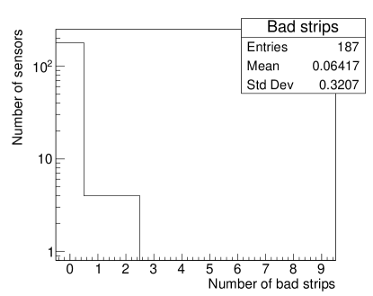
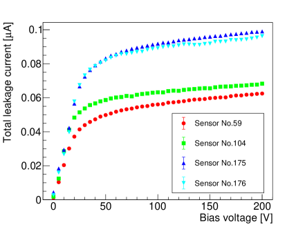
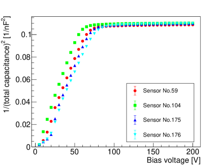
Basic performance of silicon strip sensors was measured by the manufacturer before shipment. The total leakage current and capacitance of the sensor were measured as a function of the bias voltage. Any strip defects (e.g., a shortage of AC-DC strips, or an isolation of strips) were recorded and only the sensors whose defective strip ratios were less than 5% were delivered. The full depletion voltage and the statistics of bad strips for 187 sensors measured by the manufacturer are shown in figure 7. The total leakage current and capacitance were also measured in our laboratory (figure 8) and they were consistent with the measurements by the manufacturer. The total leakage current was also measured at each step of module assembly to find any damage that appeared during assembly.
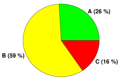
Basic performance of SliT128A chips was measured before assembly to the readout board. A probe card was used to deliver signals from a SliT128A chip and power supplies to a SliT128A chip. Quality of SliT128A chips were categorized into a rank of A, B and C. Chips without any defects are categorized as a rank A. Chips with a noise level greater than 1250 electrons on average or more than five noisy (comparator output is always high) or dead (no comparator output) channels are categorized as a rank B. Chips with severe defects such as malfunction of comparator output in more than 32 channels are categorized as a rank C. The ratio of quality of SliT128A measured for 115 chips is shown in figure 9. SliT128A chips without any defects (rank A) were used for module assembly. The same tests were performed after connecting SliT128A chips to a readout board and after connecting a sensor to SliT128A chips. The readout boards without any defective SliT128A chips were used for module assembly.
The pull test was performed on wires bonded on spare parts of detector modules prior to practical assembly. The bonding parameters were optimized to satisfy the pull strength greater than 60 mN at any bonding positions (typically, greater than 80 mN). The same bonding parameters were used at practical assembly.
4 Detector performance
4.1 Laboratory measurements
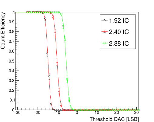
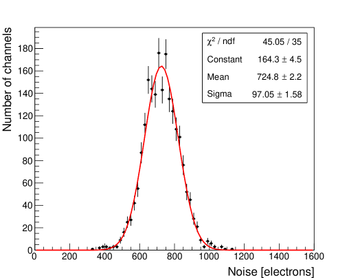
Before the test with a positron beam, the noise, the time over threshold (ToT), and the time walk of the detector module were evaluated using test pulses generated by a function generator. The noise can be evaluated from the threshold scan with different injected test pulse charges. A complementary error function is fitted to the counting efficiency as a function of the threshold voltage. The signal amplitude corresponds to the threshold at 50% efficiency and the noise level corresponds to the difference of thresholds at efficiency of 50% and 84.3%. Figure 11 shows examples of the counting efficiency curves of one readout channel. Figure 11 is the equivalent noise distribution of all readout channels in two detector modules. The mean of the equivalent noise charge (ENC) is measured to be 725 electrons with a detector capacitance of the silicon strip sensor of 17 pF. For the actual detector to be used at the J-PARC muon /EDM experiment, the detector capacitance is estimated to be about 30 pF because of a floating capacitance of long signal transport line. The dependence of the noise on the detector capacitance is evaluated to be 33 electrons/pF according to the circuit simulation. The mean of the ENC is estimated to be 1150 electrons at the detector capacitance of 30 pF.
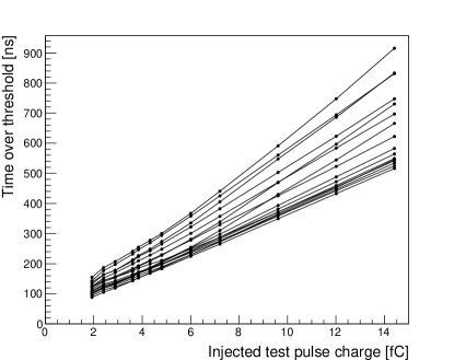
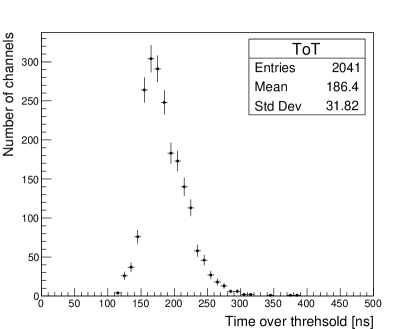
Based on the result of the threshold scan, the threshold voltage is set to match 1.15 fC which corresponds to 30% of MIP charge (3.84 fC) level in each channel. The ToT, which is the width of the comparator output, is measured as a function of the test pulse charge at this threshold. Figure 12 shows the ToT distribution with an injected test pulse charge of 3.84 fC. The mean value of the ToT is 186 ns. According to this measurement result, detectors are estimated to tolerate up to a hit rate of 5 MHz on average for a MIP charge signal.
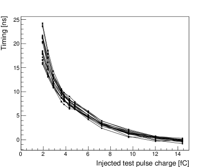
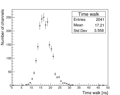
The time walk is defined as the maximum time variation in the comparator output over a signal range of 1.92-11.52 fC, with the comparator threshold set to 1.15 fC. Figure 13 shows the distribution of the time walk of two detector modules. The mean value of the time walk is 17.2 ns. This value is larger than the requirement at the J-PARC muon /EDM experiment of 1 ns. This will be solved by the next version of the front-end ASIC. Time variation due to the time walk is corrected later to improve the time resolution.
4.2 Beam test setup
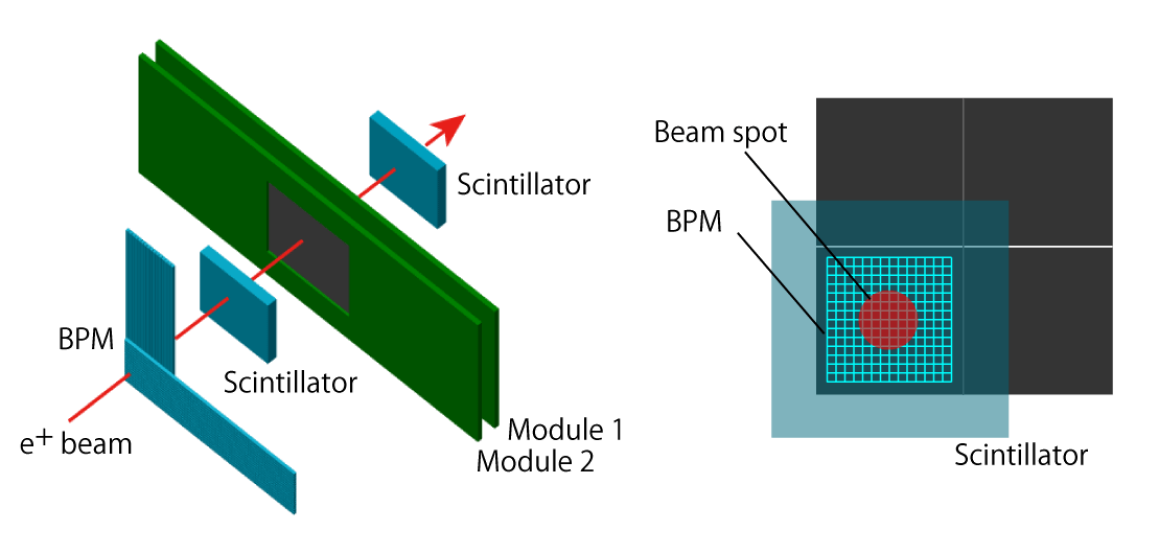
The performance of the detector modules was evaluated using a positron beam at the ELPH, Tohoku University [11]. The momentum-analyzed positron beam with the momentum of 730 MeV/ was produced from 1.3 GeV electrons by a series of reactions of Bremsstrahlung and pair production. The setup of the beam test is shown in figure 14. Two detector modules whose strip directions are orthogonal were put perpendicular to the beam axis. The module with horizontal strips (Module 1) is downstream of the beam line and the module with vertical strips (Module 2) upstream. Events were triggered by the coincidence of two scintillation detectors sandwiching the silicon strip detector modules. The size of the scintillator is 800 mm 800 mm 5 mm in width, height and thickness, respectively. The coincidence rate was about 1 kHz. For the coincidence trigger, the FPGAs on detector modules continuously send the start signals for the writing process at intervals of 50 s, which is longer than buffer length of 40.96 s. This is to avoid injecting the start signal for the writing in the state of writing process. If the FPGAs detect the coincidence trigger signal, they stop the continuous start signal for the writing process and send the start signal for the readout process. To reduce the trigger rate lower than the acceptable rate of the DAQ system, the trigger rate is prescaled to about 90 Hz. Almost only one positron hit the detector modules in one event in this condition. A beam profiling monitor (BPM) consisting of two layers of 14 scintillating fibers was installed to determine the incident position of positrons. The fiber is made from 3 mm square cross-section scintillator, and the incident position is determined with a 3 mm resolution. The center-of-the-beam position is set at the lower left of the modules as shown in figure 14 (right).
4.3 Measurement results
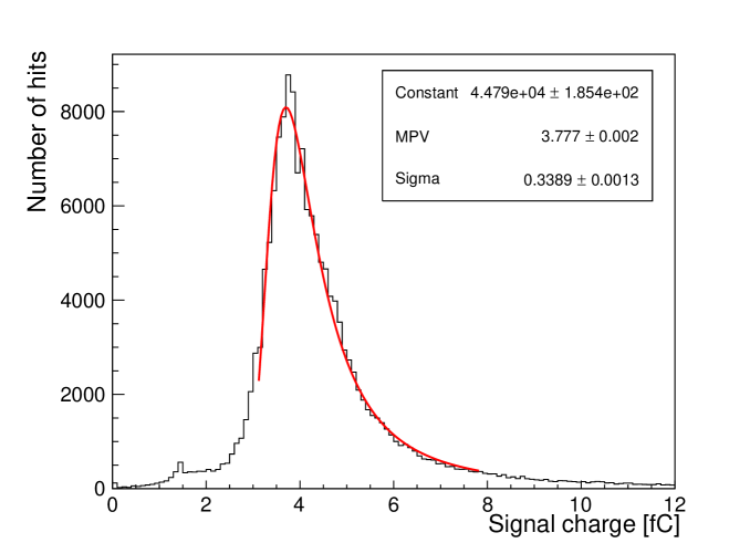
Figure 15 shows the charge distribution of the beam signal measured by two silicon strip detector modules. The most probable value (MPV) of the charge distribution is fC, which is consistent with the simulated MIP charge of 3.84 fC within an uncertainty on the charge calibration (about 2%). The signal-to-noise ratio is derived to be at the detector capacitance of 17 pF, by taking the ratio of the MPV of the charge distribution measured by the positron beam to the mean of the noise level measured by test pulses. At the detector capacitance of 30 pF, the signal-to-noise ratio is estimated to be 20.8.
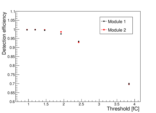
The detection efficiency is calculated by using events with hits on two layers of the BPM and no dead sensor strips or no strips connected to dead readout channels in the beam position determined by the BPM. The detection efficiency of a module is defined as the ratio of the number of events with more than one hit on two modules to the number of events with more than one hit on the other side of module. The measured detection efficiency is shown in figure 16 as a function of the threshold. The detection efficiency at a threshold of fC (about 30% of a MIP charge) is measured to be %.
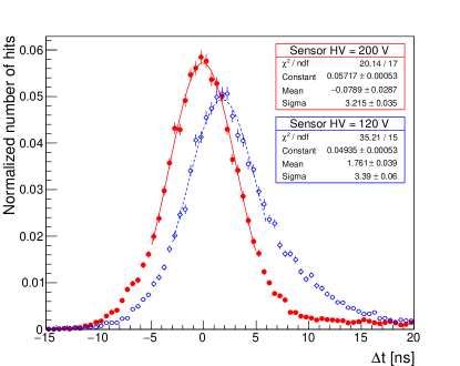
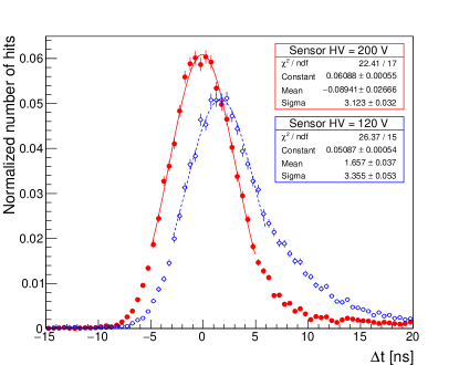
The time resolution of the detector modules is evaluated by comparing time of the signal exceeding the threshold digitized in 5 ns intervals with the trigger timing. To improve the time resolution, the timing calibration is applied based on the data with test pulses shown in figure 13. This calibration removes the time walk effect and the time difference between the channels. To study dependence of the time resolution on the bias voltage to a sensor, the detector modules are operated at the bias voltage of 120 V and 200 V. The timing distributions are shown in figure 17. The time resolution is measured to be 3.4 ns (the Module 1 and 2) as the standard deviation in the core region with a long tail distribution at the bias voltage of 120 V. At the bias voltage of 200 V, the time resolution in the core region is improved to be 3.2 ns and 3.1 ns as the standard deviation for the Module 1 and the Module 2, respectively, and there is a small distribution in the tail region.
5 Conclusions
The detector for positrons/electrons from a pulsed muon beam was developed aiming at the measurements of the muon /EDM and the muonium hyperfine structure interval at the J-PARC, and the measurement of the proton charge radius at Tohoku University. The detector is required to measure a signal charge up to four MIPs, to tolerate the hit rate of 150 kHz/mm2, to have the signal-to-noise ratio greater than 15 and time resolution much better than 2 s while it needs to store data in a period more than 10 s. The time walk over a signal range of 0.5-3 MIP charge is required to be less than 1 ns to constrain a bias on the time measurement.
The detector uses a silicon strip sensor with a 190 m strip pitch and a front-end electronics with a sampling rate of 200 MHz and a buffer memory having a depth of 8192 points. The data of one detector module in a period of 40.96 s (=8192 points 5 ns) can be read out up to a repetition frequency of 75 Hz without the zero-suppression algorithm, which is sufficient for the muon beam rate of 25 Hz at the J-PARC. Performance of fabricated detector modules was evaluated at a laboratory and a beam test using the positron beam at Tohoku University. According to the measured mean value of the ToT, detectors are estimated to tolerate up to a rate of 5 MHz for a MIP charge signal while the maximum hit rate is estimated to be 1.4 MHz for the strip size of this sensor. The signal-to-noise ratio is estimated to be 20.8 on average for a MIP charge signal at the actual detector for the J-PARC muon /EDM experiment. The detection efficiency is measured to be % at a threshold of 1.19 fC. The time resolution is measured to be 3.2 ns as the standard deviation in the core of the distribution when the bias voltage to a sensor is 200 V. These results satisfy the requirements of the detector. The time walk is measured to be 17.2 ns on average and it is larger than the requirement. This will be solved by the next version of the front-end ASIC.
Acknowledgments
The authors would like to thank the KEK and the J-PARC muon section staffs for their strong support, the Open Source Consortium of Instrumentation (Open-It) of KEK for their support on the electronics design, and Simon Eidelman at Budker Institute of Nuclear Physics and Novosibirsk State University for his diligent proofreading of this article. This work is supported by JSPS KAKENHI Grants No. JP15H05742 and JP16H06340.
References
- [1] Y. Miyake et al., Current status of the J-PARC muon facility, MUSE, J. Phys.: Conf. Ser. 551 (2014) 012061.
- [2] N. Kawamura et al., New concept for a large-acceptance general-purpose muon beamline, Prog. Thoer. Exp. Phys. 2018 (2018) 113G01.
- [3] M. Abe et al., A new approach for measuring the muon anomalous magnetic moment and electric dipole moment, Prog. Theor. Exp. Phys. 2019 (2019) 053C02.
- [4] G. W. Bennett et al. (Muon () Collaboration), Final report of the E821 muon anomalous magnetic moment measurement at BNL, Phys. Rev. D 73 (2006) 072003.
- [5] J. Grange et al. (E989 Collaboration), Muon () Technical Desgin Report, arXiv:1501.06858.
- [6] K. Shimomura, Muonium in J-PARC; from fundamental to application, Hyperfine Interact. 233 (2015) 89–95.
- [7] T. Suda et al., Measurement of Proton Charge Radius by Low-Energy Electron Scattering, J. Particle Accelerator Society of Japan 15 (2018) 52–59.
- [8] T. Uchida, Hadware-Based TCP Processor for Gibabit Ethernet, IEEE Transactions on Nuclear Science 55 (2008) 1631–1637.
- [9] Y. Yasu et al., A Data Acquisition Middleware, in 2007 15th IEEE-NPSS Real-Time Conference, (Batavia, IL, USA), pp. 1–3, 2007. DOI.
- [10] Y. Yasu et al., Development of DAQ-Middleware, J. Phys. Conf. Ser. 219 (2010) 022025.
- [11] T. Ishikawa et al., A detailed test of a BSO calorimeter with 100-800 MeV positrons, Nucl. Instrum. and Meth. A 694 (2012) 348–360.