Theory and Design of Multifunctional Space-Time Metasurfaces
Abstract
Integrating multiple functionalities into a single metasurface is becoming of great interest for future intelligent communication systems. While such devices have been extensively explored for reciprocal functionalities, in this work, we integrate a wide variety of nonreciprocal applications into a single platform. The proposed structure is based on spatiotemporally modulated impedance sheets supported by a grounded dielectric substrate. We show that, by engineering the excitation of evanescent modes, nonreciprocal interactions with impinging waves can be configured at will. We demonstrate a plethora of nonreciprocal components such as wave isolators, phase shifters, and circulators, on the same metasurface. This platform allows switching between different functionalities only by modifying the pumping signals (harmonic or non-harmonic), without changing the main body of the metasurface structure. This solution opens the door for future real-time reconfigurable and environment-adaptive nonreciprocal wave controllers.
I Introduction
The next generations of communication systems will need multifunctional devices that adapt to different usage and environment requirements, enhancing user experiences and providing better information exchange. In this emerging paradigm, due to their integration capabilities and the unprecedented opportunities for controlling waves, metasurfaces are positioned as the platform of choice to implement multifunctional responses. By varying the local properties of each composing element in space and time, one can create metasurfaces with different scattering responses. Metasurfaces can be treated as multi-port devices that are able to simultaneously control waves incoming and outgoing from/to a number of propagation directions, for example, waves coming from oppositely tilted angles [1, 2]. Following the classical notation of multi-port networks, the properties of a metasurface can be modeled by the scattering matrix, where each element represents the ratio of the flux amplitudes between the outgoing waves to -port and the incoming wave from -port. Assume that there is no frequency transformations during scattering, the functionalities of metasurfaces can be classified into two groups: reciprocal, characterized by symmetric scattering matrices , and non-reciprocal, where scattering matrices are asymmetric
Reciprocal metasurfaces have been intensively studied in the last decade. In practice, one can make use of gradient or space-modulated metasurfaces for tailoring the scattering properties between different ports and design anomalous reflectors [3, 4, 5], beam splitters, multichannel retroreflectors [1] or asymmetric absorbers [2]. Recent advances in reciprocal metasurfaces have shown that one metasurface can perform a multitude of functionalities, switching from one application to another by reconfiguring electromagnetic parameters of the individual meta-atoms. For example, in [6], independent tunability of resistance and reactance of each unit cell using embedded tunable circuits has been discussed. In this way, by locally modifying the impedance of each unit cell, the metasurface can act as a perfect absorber or anomalous reflector without changing the main body of the metasurface structure.
Reciprocity imposes certain restrictions in the design of metasurfaces, and there are practical applications where it is necessary to go beyond them. Traditionally, this goal has been achieved with magneto-optical materials, such as ferrites [7] and graphene [8, 9, 10], biased by external static or slowly-varying magnetic fields. But the use of bulky magnets makes these devices incompatible with integrated technologies. In addition, the weak magnetic response and high losses in terahertz and optical ranges further inhibit their use in future optoelectronic and nanophotonic systems. One magnetless alternative is to embed nonlinear materials in resonant cavities [11, 12, 13]. By creating spatial asymmetries in the cavity, the distribution of electromagnetic fields can be made significantly different for opposite illuminations. However, this solution is restricted to strong excitation intensities, poor isolation, and nonsimultaneous excitation from different ports [14, 15].
In recent years, dynamic modulation of material properties has attracted considerable attentions in both physics and engineering communities, due to its great potentials to induce extraordinary wave phenomena [16, 17, 18, 19, 20, 21, 22]. Time-varying materials break Lorentz reciprocity in linear and magnet-free devices. Spatiotemporal modulation can impart synthetic linear or angular momentum in the operating systems that emulate high-speed mechanical motion, and therefore produce Doppler-like nonreciprocity [23, 24, 25]. Based on this principle, many interesting phenomena have been explored [26], such as wave isolation [27, 28, 29, 30, 31, 32, 33, 34, 35] and circulation [36, 37], one-way beam splitting [38], frequency conversion [39, 40, 41], and nonreciprocal antennas [24, 42, 43, 44]. However, the nonreciprocal applications are usually fixed and unadaptable to changing environments or application requirements. While the existing works mostly focus on a specific nonreciprocal effect realized with a fixed modulation scheme, in this paper, we show that it is possible to develop robust and general means for reconfigurable nonreciprocal functionalities on a metasurface platform.
In particular, we demonstrate that by altering the space-time modulation functions it is possible to implement various canonical nonreciprocal devices on a universal platform. This multifunctional platform is based on a tunable surface impedance sheet supported by a metallized substrate. We assume that the resistance and reactance of the surface impedance can be independently and locally controlled in real time [6]. We first develop a generalized circuit theory to characterize the scattering harmonics of surface impedances modulated with arbitrary traveling waveforms (Section II). The theoretical formulation allows not only direct computations of scattering harmonics for a known modulated surface impedance, but also finding the optimal surface impedance that ensures excitation of a prescribed set of scattering harmonics. By incorporating evanescent fields into the picture, the optimized surfaces exhibit strong and controllable nonreciprocity. Based on this principle, we assign optimal modulation functions to a single metasurface with fixed dimensions and demonstrate possibilities to realize isolators, phase shifters, quasi-isolators, and circulators (Section III). In addition, we propose viable practical implementation schemes at different frequency ranges, showing realizability of the proposed multifunctional and adaptable platform (Section IV).
II Generalized Circuit Theory for Space-Time Modulated Surfaces
In this section, based on the surface impedance model, we present the theoretical formulation that describes a reconfigurable platform for nonreciprocal devices. We consider the structure shown in Fig. 1: an electrically thin sheet mounted on a grounded substrate. The main goal is to allow arbitrary reconfiguration of the nonreciprocal functionality using spatiotemporal modulations of the electric response of the sheet.
For a general impedance sheet, its electrical properties can be defined by the parallel connection of a conductance, , and an inductance, , which are periodically modulated in space and time [see Fig. 1] with spatial frequency ( is the spatial period of modulation functions) and temporal frequency ( is the temporal period of modulation functions). We assume that and are modulated with an arbitrary traveling waveform (the inverse of inductance, , is introduced in this paper for mathematical simplicity), and therefore they can be expressed as a sum of Fourier series [45, 46],
| (1) |
where denotes either or , and represents and which are the harmonic coefficients of and , respectively. It is important to notice that to ensure that both and are real-valued functions.
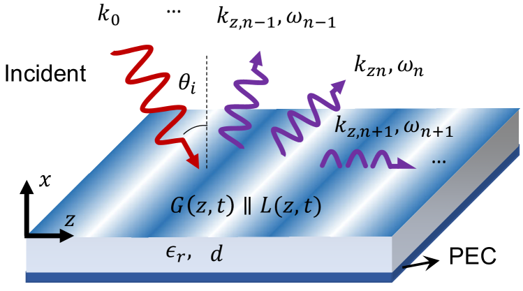
Then, if a plane wave (wavenumber and frequency ) impinges on the structure at the incidence angle , according to the Floquet-Bloch theorem, the scattered fields contain an infinite number of Floquet harmonics. The -th harmonic propagates with the transverse wavenumber and has the frequency [45]. We write the tangential components of the total electrical and magnetic fields on the surface as a sum of the incident wave and all the scattered harmonics:
| (2) |
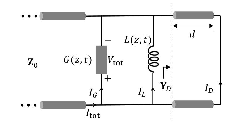
The coefficients and can be uniquely determined by enforcing the boundary conditions on all the interfaces of the structure [see Fig. 1]. However, this could be a cumbersome task, especially for structures with multiple constitutive layers. To simplify the mathematical derivations, we analyze the metasurface using the transmission-line model shown in Fig. 1. In this model, the spatiotemporally varying sheet is represented by a shunt impedance formed by a parallel connection of an inductor and a resistor. The metal-backed substrate is modeled as a section of transmission line with the length equal to the substrate thickness. The infinitely extended transmission line on the left side of Fig. 1 represents free space, and its characteristic impedance, denoted as , is the characteristic impedance of plane waves in free space. It should be noted that the effect of periodic modulation results in the matrix representation of all circuit components (explained in the following text). The tangential components of the total electric and magnetic fields on the surface are analogous to the total voltage and current in the circuit ( and ). From (2) we see that the voltage is composed of infinitely many harmonics:
| (3) |
The total current is a superposition of all currents flowing in the conductance, inductance, and the shorted transmission line: . The partial current in each circuit component is also a sum of an infinite number of Floquet harmonics,
| (4) |
Unlike the stationary scenario (without spatiotemporal modulation), in space-time modulated systems, and cannot be simply related by a scalar impedance or admittance. Instead, one must consider all the harmonics from to . Practically, we only take a finite number of harmonics from to into consideration ( is large enough to ensure the convergence of harmonics). The voltage and current at each element can be written as dimensional vectors: and . These voltage and current vectors can be related by an admittance matrix
| (5) |
Next, using the linear relations between voltage and current vectors, we find the admittance matrix for each lumped component in the circuit. The current flowing in the conductance reads
| (6) |
After substituting Eqs. (1), (3), and (4) into Eq. (6), we have
| (7) |
Using the change of variable , the -th current harmonic can be written as
| (8) |
We can see that the current harmonics are not only induced by the -th voltage harmonic, but also contributed by coupling with other harmonics. Equation (8) must be satisfied for all harmonics, generating a system of equations formed by linear equations (). The equations can be written in the matrix form , which can be expanded as
| (9) |
Here, is called admittance matrix. It should be noted that is a Toeplitz matrix with elements , where are the row and column indexes of the matrix, respectively.
Following a similar approach, we derive the admittance matrix for the space-time modulated inductance. The time-domain relation between the current and voltage across a time-varying inductor reads
| (10) |
After substituting Eq. (1) and Eq. (4) into Eq. (10) and using the same mathematical treatments in Eq. (7), we can find the admittance matrix of inductance, which is filled by matrix element [45].
Finally, we need to calculate the admittance matrix of the shorted transmission line, . One must notice that different Floquet modes have different frequencies and propagation constants in the substrate. Since the substrate is not modulated, there are no coupling elements in . Therefore, is a diagonal matrix with elements , where is the input admittance of shorted transmission line for -th harmonic. Following the derivation in the textbook [47, § 2.7], we can obtain the expression of [45],
| (11) |
where is the normal component of the wavenumber in the dielectric substrate and is the TM-wave impedance of dielectric substrate.
After the admittance matrices for all the circuit components are determined, the total admittance is defined as . This matrix relates the total current and voltage (summation of the incident and reflected harmonics) of the circuit:
| (12) |
where the superscripts ‘in’ and ‘re’ stay for the incident and reflected harmonics, respectively. The tangential electrical and magnetic fields of the incident and scattered harmonics are related by the characteristic impedance matrix of free space . For TM incidence, the impedance is a diagonal matrix filled with , where is the vertical wavevector of -th harmonic. Therefore, we have
| (13) |
Substituting (13) into (12), we can find . The parameter is called the reflection matrix and is given by
| (14) |
where is the unity matrix. The source vector is defined as . We can see that the -th reflected harmonic is equal to the matrix element located at the -th row and -th column of the reflection matrix , .
If the surface conductance and inductance in Fig. 1 and the substrate properties are known, for a specific plane wave excitation the scattering harmonics are uniquely determined by Eq. (14). Alternatively, for desired scattering responses, it is also possible to find properly modulated conductance and inductance that correspond to the generation of the desired scattering harmonics by the metasurface. However, there is no simple analytical formulation that could directly determine the modulation functions for a set of desired scattering harmonics. For this reason, we mathematically optimize the Fourier coefficients of the modulation functions and until they generate the wanted harmonics for two opposite incident directions ( and ), realizing desired nonreciprocal effects.
III Engineering Nonreciprocity of Space-Time Modulated Metasurfaces
In this section, we show that the generalized circuit model developed in Section II can be used to realize different nonreciprocal devices engineering modulation functions. As examples, we design isolators, nonreciprocal phase shifters, quasi-isolators, and circulators on a physically rigid platform, only by modifying the modulation functions.
III.1 Metasurface Isolators
An isolator is a lossy, passive, and matched two-port device that allows unidirectional wave transmission [47]. For a perfect isolator, waves incident on one port are fully dissipated while the waves incident on the second port are fully transmitted without frequency conversion. The scattering matrix of an ideal isolator is defined as
| (15) |
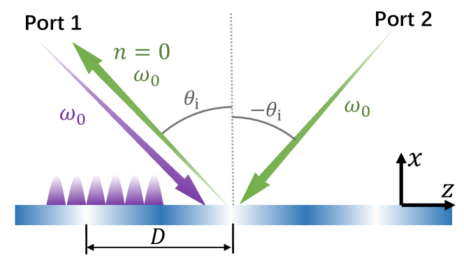
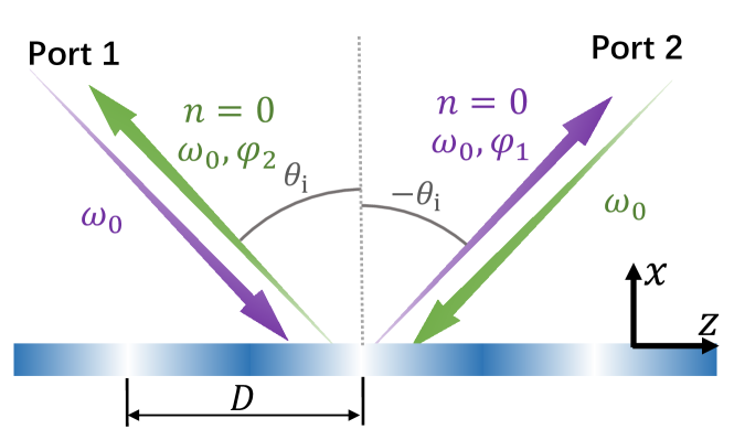
Figure 2 shows the design principle of the metasurface isolator. Plane waves incident at (Port 1) are completely absorbed, while waves incident at (Port 2) all are specularly reflected into Port 1 (). It is important to notice that, according to this definition, there is no frequency conversion between ports.
Wave isolation realized with space-time modulated media has been demonstrated in a few papers [48, 32, 36, 30], where the classical scattering matrix [see Eq. (15)] is not suitable to describe those systems. In those works, the incident wave from the attenuation port is not absorbed due to material losses but converted to higher-order harmonics and transmitted, requiring absorptive filters to remove the generated harmonics. In another work [35], although there is no frequency conversion of the scattered propagating waves, the waves incident from the attenuation port are not actually absorbed but leak away through other ports (transmission side). Here, we propose a solution based on a lossy gradient surface impedance that allows us to design isolators according to the classical definition shown in Eq. (15). The design methodology consists of three steps.
Step 1: Making use of the multi-channel metasurface concept, the first step in the design is to find the period of the metasurface space modulation that allows the required propagating channels. In this case, the two-port system will be implemented in the metasurface platform by the incident direction and the specular reflection, as it is shown in Fig. 2. This condition can be fulfilled by restricting the spatial period as [45]. In addition, this periodicity ensures that both and are zero (no retroreflection or other higher order diffraction modes).
Step 2: Once the spatial period of the metasurface has been chosen, the second step is to find a proper traveling-wave modulation profile that can realize perfect absorption for plane-wave incident from (Port 1). We define the frequency of incidence as , and the modulation frequency is . For total absorption at Port 1, the scattered field should have no specular reflection which means
| (16) |
should be satisfied for incidence of . Next, we ensure strong evanescent fields are excited simultaneously, which is the key point of this design method. The reason for the excitation of evanescent fields includes: (1) the wavelength of these fields are much smaller than the spatial modulation periodicity, and they are generated in order to locally satisfy the gradient impedance boundary condition. Therefore, they tend to be sensitive to the surface boundary perturbation, as well as the incident angles; (2) the amplitudes of evanescent fields can control the resonance strength. To warrant the excitation of evanescent fields, we impose,
| (17) |
Notice that we only need to ensure the desired amplitude of the first-order evanescent mode (). Eq. 16 and Eq. 17 are called objective functions that guarantee evanescent fields induced absorption at Port 1.
Next we aim to find the optimal surface impedance that can satisfy these two objectives. From the results of Section II we know that are determined by the Fourier coefficients of and . In order to find and that satisfy the objectives, we can introduce unlimited numbers of and in Eq. (1). However, we assume that only three Fourier terms are enough to adequately describe each component [ for and for ]. Without loosing generality, we also assume that and (this assumption always holds in the following text), such that the Fourier terms are real numbers and both and are even functions with respect to the -axis. Under these assumptions, the Fourier series for and in Eq. (1) are reduced to
| (18) |
and
| (19) |
At this point, in order to preserve the physical meaning of the model, one must ensure that the conductance and inductance are always positive along the -axis. To do that, two additional constraints are introduced, and .
In total, there are two objective equations and two linear constraints to be considered with four unknown Fourier coefficients. To solve this optimization problem, we use MATLAB Optimization Toolbox to find the solutions of (16) and (17), using the optimization function (optimization code is available in [45]). Table 1 shows the optimized and for different evanescent mode amplitudes.
| Evanescent field | (dB) | (dB) | ||||
| 208.15 | -38.1 | 43.36 | -11.42 | -21.6 | -83 | |
| 26.17 | -5.50 | 36.03 | -3.46 | -5.37 | -64 | |
| 2.29 | -0.67 | 35.25 | -1.03 | -0.08 | -43.7 |
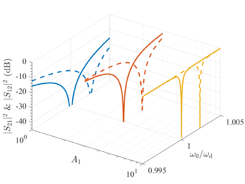
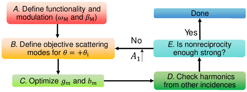
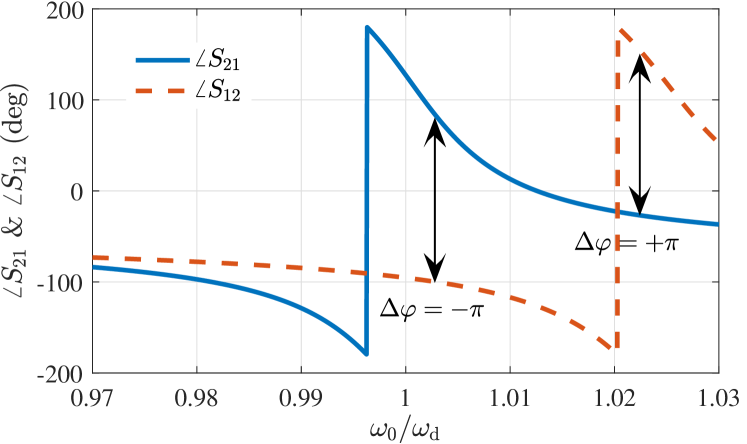
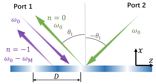
Step 3: Once the surface impedance satisfying the objective functions at has been optimized, we examine its scattering fields for using the mode matching method presented in Section II. For incidence from Port 2, the resonance shifts to higher frequency (dashed line in Fig. 3). The space-time modulated surface emulates a moving slab with velocity of along the direction. Effective motion of the metasurface compromises the established phase matching of the incident plane wave and one of the surface modes (as deigned at Step 2). For incidence from Port 2, the phase matching condition holds at lower frequencies. This effect is similar to the phenomenon in [35], based on asymmetric distortion of the dispersion diagram under travelling-wave modulation. For the case of , although nonreciprocity is achieved, the isolation performance at the defined frequency is not good, since the wave incident from port 2 is almost absorbed ( dB). To obtain near perfect isolation, the amplitude of evanescent field should be further improved. We see that as increases, the resonance become stronger. When (yellow curves), near-perfect isolation is achieved at . In this case, wave incident from Port 1 is completely absorbed while from Port 2 it is fully delivered to Port 1 (the efficiencies of both absorption and transmission are above 99 %). The above design procedures are summarized in Fig. 4: we first optimize the modulation functions that ensure the desired propagation modes as well as the evanescent modes for the forward direction (Steps A-C). Then, we examine the scattered harmonics for the backward direction and check the achieved level of nonreciprocity (Step D). If the nonreciprocity is not strong, we further enhance the amplitude of evanescent mode defined in Step B and optimize the modulation function until it satisfies the desired nonreciprocal functionality. In the next subsections, based on this design procedure, we realize and engineer other nonreciprocal functionalities on the same physical platform.
III.2 Metasurface Nonreciprocal Phase Shifters
In lossless nonreciprocal phase shifters, the phase shifts for waves traveling between their two ports in opposite directions differ by a specific phase difference . The scattering matrix of a lossless and matched phase shifter can be generally represented as
| (20) |
The schematic of the proposed nonreciprocal metasurface phase shifter is shown in Fig. 5. Light incident from (Port 1) is fully reflected (that is, transmitted into Port 2) with the transmission phase , while from the opposite direction (Port 2), the transmission phase is .
As far as we know, space-time metasurfaces providing nonreciprocal phase shifts for free space propagation have not yet been reported. Here, we demonstrate that engineering induced evanescent fields it is possible to create metasurface phase shifters with controllable differential phases. The proposed design methodology consists of the following steps.
Step 1: Similarly to the design of metasurface isolators, the period of the metasurface phase shifter is selected within the range to allow only specular reflection. This condition will warrant .
Step 2: Next, we ensure proper excitation of resonant evanescent fields for incidence of . As we know from the design principle of the metasurface isolator (Section III.1), such resonance is very sensitive to the transverse unidirectional modulation momentum and the resonance frequency is expected to shift at the opposite incidence (). Following this idea, we introduce one objective function at , which guarantees that the first order evanescent field is excited with amplitude . Since the system is required to be lossless, the surface conductance is removed (), and only the inductance is subject to modulation. We assume a simple harmonic modulation waveform on
| (21) |
where . Notice that the constraint should be imposed to warrant that the inductance values remain positive. Using optimization, a proper set of and can be found to make sure that (as an example). We can see from Fig. 6 (blue solid line) that the transmission phase has an abrupt change around the defined resonant frequency .
Step 3: After obtaining the optimal surface impedance, we investigate its transmission phase for the opposite incidence. Similar to the case of metasurface isolators (see Section III.1), sharp resonance in the phase spectrum shifts to higher frequency, creating a large phase difference at a fixed frequency. For example, at and , the devices exhibits and phase shifts for waves traveling in the opposite directions, which can be practically used as a gyrator. The phase shift is continuously tunable by increasing or decreasing the modulation frequency, which adjusts spectral distances of the two resonances. The frequency bandwidth of such phase shifters depends on the quality factor of the resonance which is determined by . Decreasing and increasing the modulation frequency we can obtain a more flat phase curve which effectively expands the frequency bandwidth.
III.3 Metasurface Quasi-Isolators
In Section III.1, we have shown how one can realize wave isolators using lossy modulated impedance sheets and demonstrated near perfect isolation without the need of frequency filters. Here, we show that wave isolation can be realized also in lossless two-port systems, as schematized in Fig. 7. Instead of being absorbed, as in usual isolators, the energy from Port 1 is fully reflected black (retro-reflection) with a frequency conversion , while the energy from Port 2 is fully delivered to Port 1 (specular reflection) without frequecny conversion . It is important to notice that, although frequency conversion occurs when the system is illuminated from Port 1 , this higher-order harmonic is not delivered to Port 2 and, for this reason, frequency filters are still not necessary. These devices provide the same functionality as ideal isolators if one considers the signal frequency, and therefore we call them as quasi-isolators. Note that ideal lossless isolators without frequency conversion or conversion to some other mode or channel are forbidden by energy conservation. The design of these devices has two steps.
Step 1: The first step is to define the spatial period of the metasurface that allows not only specular reflection but also retro-reflection. This requirement can be satisfied choosing . In this case, we still create a two-port system, but the incident waves are allowed to reflect back into the same port (retro-reflection). Notice that the difference with the lossy isolator where the condition was automatically fulfilled by choosing the period which does not allow propagation of any diffracted mode, including the retro-reflected one.
Step 2: The second step is to realize perfect retro-reflection for incidence from Port 1 () at the target frequency . Notice that in the case of ideal retro-reflection the energy transmitted to Port 2 is zero due to energy conservation. In addition, the evanescent fields should be specified to control the -factor of the system. Taking these factors into considerations, we define two objectives for incidence from :
| (22) |
Combining these objectives with the linear condition that warrants only positive values of the inductance, , one can see that at least three degrees of freedom are required for specifying the system. For this reason, three unknowns (, , and ) are introduced to synthesize . We can write the expression for as
| (23) |
where modulation frequency is assumed in this example. Using optimization tools, we find the Fourier coefficients for three different values of , shown in Table 2.
| Evanescent field | (dB) | (dB) | |||
| 229.83 | 30.19 | -37.70 | -15.73 | -81.87 | |
| 192.52 | 12.34 | -13.86 | -2.41 | -46.02 | |
| 187.79 | -6.30 | 6.13 | -0.04 | -42.42 |
Figure 8 presents the scattered harmonics at two opposite incidence for two optimal surfaces. The first panel shows the results for . We can see that the harmonics excited by plane waves at Ports 1 and 2 (incidence angles and ) are almost identical, meaning that if the amplitude of the first-order evanescent harmonic is so small, there is no significant phase mismatch for excitation from the other port. Therefore, waves incident on both ports are reflected back into the same port. However, as increases, the enhanced resonance of evanescent fields becomes more sensitive to the angle of illumination. For the case when , the excited evanescent modes are completely different for illuminations from the opposite angles, which leads to enhanced transmission from Port 2 to Port 1 and realization of the quasi-isolator regime. These results again show that we can impose strong evanescent fields (improve -factor) to achieve evident efficiency of the nonreciprocal devices.
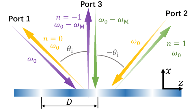
III.4 Metasurface Circulators
With the proper choice of spatial period and using more complex time-modulation function, it is possible to control nonreciprocal wave propagation between more ports. As a particular example, we use the design method explained above to realize three-ports metasurface circulators. Figure 9 shows the schematics of the proposed metasurface circulator, where the incident wave travels unidirectionally between three ports: 1 3, 3 2, and 2 1. It is important to note that the device introduces frequency down-conversion () for propagation from 1 3, and up-conversion () for propagation from 3 2. A similar functionality has been realized in a recent work [36] exciting two independent optical modes with transition momentum (, ) in the dispersion diagrams and creating a high-quality resonator system. However, the known design method needs careful numerical optimizations of the band structures to ensure proper support of multiple optical modes. In addition, these optical modes should be tailored to be strongly resonant (high ), to spectrally resolve them.
Here, we show that using the mode-matching method and mathematical optimization one can easily find surface impedances that realize perfect wave circulation, thus avoiding complicated band structure engineering. The design methodology for metasurface circulators consists of two steps.
Step 1: First, we increase the spatial period of the metasurface to . This periodicity allows propagation of two additional diffracted modes for the incidence angle of (wave from Port 1 can be retro-reflected or delivered to Port 3), so that the metasurface can be viewed as a three-port system (see Figure 9).
Step 2: The second step is to find the modulation functions for the metasurface circulator design. Enforcing that waves incident from Port 1 are fully directed to Port 3 and considering that the system is space-time modulated (), the amplitude of the diffraction mode should be due to the energy conservation principle [4]. This condition automatically ensures photonic transition between two different optical modes as [36] aims to achieve. Then we prescribe the amplitude of the first-order evanescent field harmonic as , to control the quality factor of the system.
In the system optimization we define two objectives corresponding to the above requirements for harmonics. However, we should notice that, as the number of ports increases, the positive-inductance condition is more difficult to satisfy if we only introduce a few Fourier terms in the modulation function. For this reason, more Fourier harmonics are included in to provide more freedoms in the construction of a purely inductive modulated sheet impedance. In particular, we introduce five unknowns in :
| (24) |
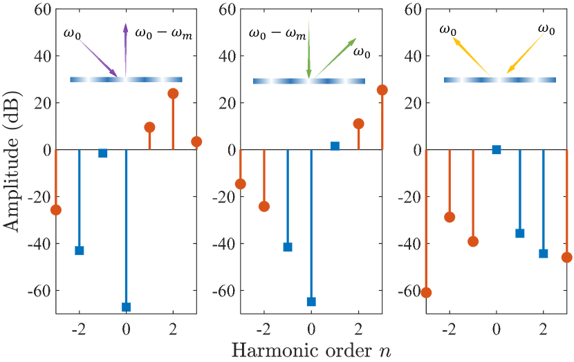
Next, the Fourier harmonics of are optimized, and the resulting values for the harmonics are summarized in the caption of Fig. 10.
Now, we examine the scattering harmonics when the circulator is illuminated from each of the three ports. The results are shown in Fig. 10. In the first scenario (left panel in Fig. 10), the wave incident from is fully delivered to the normal direction (Port 3) with strong evanescent fields excited on the surface. In the second scenario (middle panel in Fig. 10), the wave incident from Port 3 goes to Port 2 and excites the same sets of evanescent fields with scenario 1. This behavior is ensured by the phase matching condition established for scenario 1. Finally, for the wave incident from (Port 3), the incident wave propagates in the opposite direction with the modulation wave. Due to the strong phase mismatch, the resonance disappears and the device behaves as a normal mirror with full transmission to Port 1.
As the number of channels increases, more Fourier harmonics should be incorporated in the design of the modulation function, which opens up the possibility to realize wave circulation between five or more ports.
IV Possible Implementations in microwave and terahertz ranges
In Section III we have demonstrated that various nonreciprocal functionalities can be realized within the proposed space-time modulated surface impedance platform. Surface impedance is one of the most commonly used models for the design of metasurfaces, see e.g. [49, § 2.4.3]. Required surface impedance can be implemented by structuring a metallic layer into periodic patterns [50, 2]. Dynamical modulation of surface impedance can be realized by embedding tunable elements or materials in meta-atoms (unit cells of the metasurface), e.g. [51]. In microwave and millimeter-wave bands, surface impedance of meta-atom arrays can be controlled by varactors and varistors. This method has been experimentally demonstrated in the design of tunable reciprocal metasurfaces [52, 53, 54], as well as nonreciprocal space-time devices by modulating varactors in a travelling-wave form [24, 44, 33]. In the terahertz range, tunable lumped components are not practical to use due to the reduced footprint. Graphene, a two-dimensional material with gate-controlled surface impedance, can be used for realization of spatiotemporal surface impedances due to its gate-controlled sheet impedance. In this section, we discuss implementation possibilities of the proposed multifunctional platform, based on tunable lumped components in the microwave band and graphene in the terahertz band.
IV.1 Implementation Based on Reconfigurable Intelligent Surfaces
With modern integrated-circuit technology, both varactors and varistors can be packaged inside a single chip and their values can be independently controlled by external signals [55]. The control chip is then connected to each meta-atom to dynamically modify the local surface resistance and reactance of metasurfaces. The schematic of a suitable hardware platform has been proposed in [56, 57]. Meta-atoms are formed by four patches and each of them is pinned to the other side of metasurfaces and connected to controller chips (see Fig. 1 in [56]). The ground plane is positioned between the patch layer and the chip layer, which reduces interactions between electromagnetic waves and control circuitry. The chips are connected with each other by signal lines. With proper dictations from the computer, the meta-atoms are properly modulated [58], to control the effective surface impedance of each element. Such modulation platform has been utilized to achieve reconfigurability of reciprocal metasurfaces [6] where the electrical properties of the surface is modulated in space. By applying a time-varying control signal upon each chip, the surface impedance of the metasurface can be spatiotemporally modulated and the modulation function can change in time to provide multiple nonreciprocal functionalities as required.
It is worth to mention that in the theoretical model presented here we assume the modulation of inductance, but in practical implementation it is usually easier to realize temporal modulation of capacitance than inductance. The design equations for capacitive reactance can be derived in the same way as shown above for inductive sheets. Alternatively, it may be reasonable to mimic time-varying inductance using a large fixed inductance in series with a time-modulated capacitance of the control chip. In this way, the total reactance is inductive and modulated in time, producing the same effect as a time-varying inductance.
IV.2 Implementations Based on Graphene Platform
In the terahertz and mid-infrared band, graphene is a good candidate to implement the tunable component of space-time modulated metasurfaces due to its tunable electrical conductivity and the compatibility with the advanced nanofabrication technologies [39, 30, 31, 43, 40]. Considering that graphene is a lossy material, in this section we show how one can use space-time modulated graphene sheets to create tunable wave isolators in the terahertz range.
It is known that the sheet conductivity of graphene can be effectively modified via electrical bias or optical pumping. This provides the possibility of synthesizing space-time modulated surface impedances by locally varying the bias voltage applied on graphene. The sheet conductivity of graphene in the low terahertz range can be modeled as
| (25) |
where
| (26) |
is the DC conductivity, is the electron scattering time, is the electron charge, and is the Fermi level of graphene which can be controlled by the external voltage. As can be seen from Eqs. (25) and (26), graphene is naturally resistive and inductive in the terahertz range, and its sheet impedance can be expressed as . If spatiotemporally varying gate voltage is exerted on a graphene strip, both of its sheet resistance () and inductance () can be harmonically modulated with the same pumping scheme.
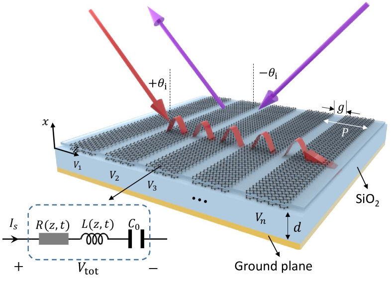
Figure 11 shows the schematic representation of the proposed design where graphene strips are periodically positioned on top of a metallized substrate. For the convenience of gating, a pair of graphene strips are separated by a thin dielectric film (e.g., ) to form a self capacitor [30]. Due to the stacked structure, the effective sheet impedance of graphene is reduced to half of the single-layer graphene impedance. Under TM polarized incidence, the electrical response of graphene patterns can be described as a series of resistance, inductance and capacitance (all of them are effective values). The static resistance and inductance of graphene without modulation are
| (27) |
where is the period of the graphene strip array, is the distance between two adjacent graphene strips, and is the structural factor which takes into account the enlargement of resistance and inductance due to the patterning of graphene [50]. The capacitance is contributed by capacitive coupling of the adjacent strips [59],
| (28) |
with the effective permittivity . Notice that Eq. (28) becomes invalid for very thin substrates (), because in this case the near-field coupling between graphene strips and the ground plane should be also considered [60]. In the present design (), Eq. (28) is valid and the capacitance is determined only by the structuring of graphene and the substrate permittivity, therefore it does not change during the modulation. A pump voltage is exerted on graphene, and the resistance and inductance of graphene are modulated around their static values. We assume the modulation function in form
| (29) |
with . Thus, the space-time lumped values are and .
The current and voltage of the series circuit are related as
| (30) |
Following the same mathematical treatment as in Section II, we obtain the coupling equation
| (31) |
where and are the th harmonic components of and , respectively. The voltage and current vectors are related by the impedance matrix, . is a matrix filled with elements
| (32) |
where is the Dirac delta function. After is known, the admittance matrix is found by inversion: . For a given grounded substrate, we can obtain its admittance matrix and further the total admittance , as explained in Section II. Finally, the scattering harmonics can be calculated from (14).
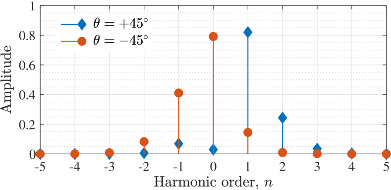
The above theory can be used for the design of wave isolators following the ideas presented in Section III.1. With a proper modulation function applied on graphene array, the incident wave can be fully converted into evanescent modes for waves from , while for the opposite tilted angle it is mostly reflected in the specular direction. To find such modulation function, we assume two unknown Fourier terms in (29), and . For a fixed modulation frequency ( GHz) and incident angle (), a set of , and (which determines the static resistance and inductance) can be optimized to fully suppress the specular harmonic and convert the incident wave into evanescent modes. Figure 12 shows that, at THz, the wave incident from is indeed transformed into the first-order evanescent harmonic with a strong amplitude of . Swapping the incident direction invalidates the phase matching condition, and, as a consequence, the evanescent amplitudes become weak. Therefore, most of the incident energy is reflected via the specular channel.
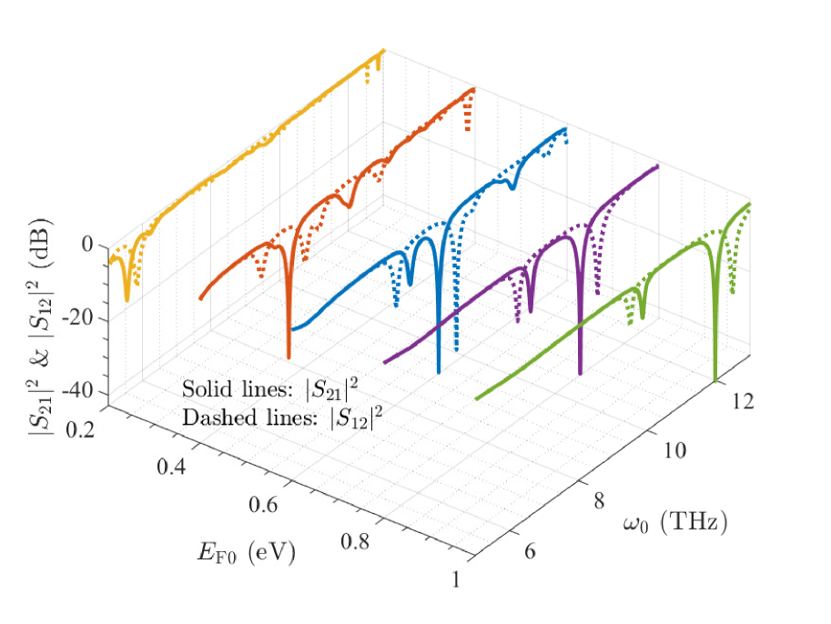
Interestingly, at other frequencies, we can always find an optimal sets of , and to reconstruct the isolation functionality. Figure 13 shows that the absorption frequency (from ) decreases as we lower the medium Fermi level of graphene . In addition, in order to achieve good isolation performance, the modulation function should be re-optimized to maximize the absorption level. Due to the modifications of the modulation function, the isolator can operate over a wide band from 5.5 THz to 12 THz without sacrificing the isolation performance.
The isolation is determined by forward attenuation as well as by reversed insertion loss. After perfect absorption is ensured in the forward direction (), the transmission for the opposite incidence is affected by the modulation speed as well as the resonance strength of the system which in fact determine the spectral distance between the two transmission minima. The resonance of the structure can be enhanced by using low resistive (high mobility) graphene. Simultaneously, reducing the resistance of graphene also helps to relax limitations on the modulation speed since the maximum modulation frequency is determined by the intrinsic time constant of graphene capacitors (, where and is the effective resistance and capacitance of the graphene gating) [61]. Theoretical estimations have shown that with high quality graphene layers, the modulation speed can reach several hundred gigahertz [62, 63]. However, in standard fabrication technology, graphene mobility significantly decreases during the fabrication process due to unavoidable impurities and contaminations from environment [64, § 1.3]. In consequence, with conventional graphene fabrication techniques, it is still a challenge to reach the modulation speed assumed in this example. On the other hand, recent advances have shown that using atomic-flat substrate (e.g., h-BN) [65], post-annealing, and improved transfer techniques [66], it is possible to obtain a high-quality graphene. In addition, the present electrical modulation might be replaced by an optical modulation scheme with significantly improved modulation speed [67, 68].
V Conclusions
In this paper, we have introduced a general approach to realize nonreciprocal metasurface devices to control waves in single or multiple scattering channels in free space. Importantly, we have shown that a variety functionalities can be realized using the same physical platform by adjusting the space-time modulation of the single tunable element: an impedance sheet. As examples, the proposed technique has been applied to design nonreciprocal metasurfaces which act as isolators, nonreciprocal phase shifters, quasi-isolators, and circulators. In addition, a graphene-based modulation platform has been proposed, where the isolation frequency can be dynamically tuned in a wide frequency range by changing the modulation function. We expect that the introduced technique can be useful in the developments of future computer-controlled intelligent nonreciprocal metasufaces for various applications.
VI Acknowledgments
This work received funding from the Foundation for Aalto University Science and Technology, the Academy of Finland (project 309421), the European Union’s Horizon 2020 research and innovation programme – Future Emerging Topics (FETOPEN) under grant agreement No 736876, and the U.S. Air Force Office of Scientific Research. The authors would thank Dr. Viktar Asadchy, Dr. Dimitrios Sounas, Dr. Fu Liu, and Dr. Beibei Kong for helpful discussions.
References
- Asadchy et al. [2017] V. Asadchy, A. Díaz-Rubio, S. Tcvetkova, D.-H. Kwon, A. Elsakka, M. Albooyeh, and S. Tretyakov, Flat engineered multichannel reflectors, Physical Review X 7, 031046 (2017).
- Wang et al. [2018a] X. Wang, A. Díaz-Rubio, V. S. Asadchy, G. Ptitcyn, A. A. Generalov, J. Ala-Laurinaho, and S. A. Tretyakov, Extreme asymmetry in metasurfaces via evanescent fields engineering: Angular-asymmetric absorption, Physical Review Letters 121, 256802 (2018a).
- Díaz-Rubio et al. [2017] A. Díaz-Rubio, V. S. Asadchy, A. Elsakka, and S. A. Tretyakov, From the generalized reflection law to the realization of perfect anomalous reflectors, Science Advances 3, e1602714 (2017).
- Asadchy et al. [2016] V. S. Asadchy, M. Albooyeh, S. N. Tcvetkova, A. Díaz-Rubio, Y. Ra’di, and S. Tretyakov, Perfect control of reflection and refraction using spatially dispersive metasurfaces, Physical Review B 94, 075142 (2016).
- Ra’di et al. [2017] Y. Ra’di, D. L. Sounas, and A. Alù, Metagratings: beyond the limits of graded metasurfaces for wave front control, Physical Review Letters 119, 067404 (2017).
- Liu et al. [2019a] F. Liu, O. Tsilipakos, A. Pitilakis, A. C. Tasolamprou, M. S. Mirmoosa, N. V. Kantartzis, D.-H. Kwon, M. Kafesaki, C. M. Soukoulis, and S. A. Tretyakov, Intelligent metasurfaces with continuously tunable local surface impedance for multiple reconfigurable functions, Physical Review Applied 11, 044024 (2019a).
- Adam et al. [2002] J. D. Adam, L. E. Davis, G. F. Dionne, E. F. Schloemann, and S. N. Stitzer, Ferrite devices and materials, IEEE Transactions on Microwave Theory and Techniques 50, 721 (2002).
- Tamagnone et al. [2016] M. Tamagnone, C. Moldovan, J.-M. Poumirol, A. B. Kuzmenko, A. M. Ionescu, J. R. Mosig, and J. Perruisseau-Carrier, Near optimal graphene terahertz non-reciprocal isolator, Nature Communications 7, 11216 (2016).
- Crassee et al. [2011] I. Crassee, J. Levallois, A. L. Walter, M. Ostler, A. Bostwick, E. Rotenberg, T. Seyller, D. Van Der Marel, and A. B. Kuzmenko, Giant faraday rotation in single-and multilayer graphene, Nature Physics 7, 48 (2011).
- Sounas and Caloz [2012] D. L. Sounas and C. Caloz, Gyrotropy and nonreciprocity of graphene for microwave applications, IEEE Transactions on Microwave Theory and Techniques 60, 901 (2012).
- Sounas et al. [2018] D. L. Sounas, J. Soric, and A. Alù, Broadband passive isolators based on coupled nonlinear resonances, Nature Electronics 1, 113 (2018).
- Mahmoud et al. [2015] A. M. Mahmoud, A. R. Davoyan, and N. Engheta, All-passive nonreciprocal metastructure, Nature Communications 6, 8359 (2015).
- D’Aguanno et al. [2019] G. D’Aguanno, D. L. Sounas, H. M. Saied, and A. Alù, Nonlinearity-based circulator, Applied Physics Letters 114, 181102 (2019).
- Shi et al. [2015] Y. Shi, Z. Yu, and S. Fan, Limitations of nonlinear optical isolators due to dynamic reciprocity, Nature photonics 9, 388 (2015).
- Sounas and Alù [2018] D. L. Sounas and A. Alù, Fundamental bounds on the operation of fano nonlinear isolators, Physical Review B 97, 115431 (2018).
- Ptitcyn et al. [2019] G. Ptitcyn, M. Mirmoosa, and S. Tretyakov, Time-modulated meta-atoms, Physical Review Research 1, 023014 (2019).
- Mirmoosa et al. [2019] M. Mirmoosa, G. Ptitcyn, V. Asadchy, and S. Tretyakov, Time-varying reactive elements for extreme accumulation of electromagnetic energy, Physical Review Applied 11, 014024 (2019).
- Sounas and Alù [2017] D. L. Sounas and A. Alù, Non-reciprocal photonics based on time modulation, Nature Photonics 11, 774 (2017).
- Yuan and Fan [2015] L. Yuan and S. Fan, Three-dimensional dynamic localization of light from a time-dependent effective gauge field for photons, Physical Review Letters 114, 243901 (2015).
- Buddhiraju et al. [2020] S. Buddhiraju, W. Li, and S. Fan, Photonic refrigeration from time-modulated thermal emission, Physical Review Letters 124, 077402 (2020).
- Koutserimpas and Fleury [2018] T. T. Koutserimpas and R. Fleury, Nonreciprocal gain in non-Hermitian time-Floquet systems, Physical Review Letters 120, 087401 (2018).
- Liu et al. [2018] M. Liu, D. A. Powell, Y. Zarate, and I. V. Shadrivov, Huygens’ metadevices for parametric waves, Physical Review X 8, 031077 (2018).
- Mock et al. [2019] A. Mock, D. Sounas, and A. Alù, Magnet-free circulator based on spatiotemporal modulation of photonic crystal defect cavities, ACS Photonics 6, 2056 (2019).
- Hadad et al. [2016] Y. Hadad, J. C. Soric, and A. Alù, Breaking temporal symmetries for emission and absorption, Proceedings of the National Academy of Sciences 113, 3471 (2016).
- Taravati and Kishk [2020] S. Taravati and A. A. Kishk, Space-time modulation: Principles and applications, IEEE Microwave Magazine 21, 30 (2020).
- Shaltout et al. [2019] A. M. Shaltout, V. M. Shalaev, and M. L. Brongersma, Spatiotemporal light control with active metasurfaces, Science 364, eaat3100 (2019).
- Yu and Fan [2009a] Z. Yu and S. Fan, Complete optical isolation created by indirect interband photonic transitions, Nature Photonics 3, 91 (2009a).
- Lira et al. [2012] H. Lira, Z. Yu, S. Fan, and M. Lipson, Electrically driven nonreciprocity induced by interband photonic transition on a silicon chip, Physical Review Letters 109, 033901 (2012).
- Yu and Fan [2009b] Z. Yu and S. Fan, Integrated nonmagnetic optical isolators based on photonic transitions, IEEE Journal of Selected Topics in Quantum Electronics 16, 459 (2009b).
- Correas-Serrano et al. [2018] D. Correas-Serrano, A. Alù, and J. Gomez-Diaz, Magnetic-free nonreciprocal photonic platform based on time-modulated graphene capacitors, Physical Review B 98, 165428 (2018).
- Qin et al. [2016] C. Qin, B. Wang, H. Long, K. Wang, and P. Lu, Nonreciprocal phase shift and mode modulation in dynamic graphene waveguides, Journal of Lightwave Technology 34, 3877 (2016).
- Chamanara et al. [2017] N. Chamanara, S. Taravati, Z.-L. Deck-Léger, and C. Caloz, Optical isolation based on space-time engineered asymmetric photonic band gaps, Physical Review B 96, 155409 (2017).
- Taravati et al. [2017] S. Taravati, N. Chamanara, and C. Caloz, Nonreciprocal electromagnetic scattering from a periodically space-time modulated slab and application to a quasisonic isolator, Physical Review B 96, 165144 (2017).
- Taravati [2017] S. Taravati, Self-biased broadband magnet-free linear isolator based on one-way space-time coherency, Physical Review B 96, 235150 (2017).
- Hadad et al. [2015] Y. Hadad, D. Sounas, and A. Alù, Space-time gradient metasurfaces, Physical Review B 92, 100304 (2015).
- Shi et al. [2017] Y. Shi, S. Han, and S. Fan, Optical circulation and isolation based on indirect photonic transitions of guided resonance modes, ACS Photonics 4, 1639 (2017).
- Estep et al. [2016] N. A. Estep, D. L. Sounas, and A. Alù, Magnetless microwave circulators based on spatiotemporally modulated rings of coupled resonators, IEEE Transactions on Microwave Theory and Techniques 64, 502 (2016).
- Taravati and Kishk [2019] S. Taravati and A. A. Kishk, Dynamic modulation yields one-way beam splitting, Physical Review B 99, 075101 (2019).
- Salary et al. [2018a] M. M. Salary, S. Jafar-Zanjani, and H. Mosallaei, Time-varying metamaterials based on graphene-wrapped microwires: Modeling and potential applications, Physical Review B 97, 115421 (2018a).
- Salary et al. [2018b] M. M. Salary, S. Jafar-Zanjani, and H. Mosallaei, Electrically tunable harmonics in time-modulated metasurfaces for wavefront engineering, New Journal of Physics 20, 123023 (2018b).
- Hadad and Sounas [2019] Y. Hadad and D. Sounas, Space-time modulated loaded-wire metagratings for magnetless nonreciprocity and near-complete frequency conversion, arXiv preprint arXiv:1906.00215 (2019).
- Taravati and Caloz [2017] S. Taravati and C. Caloz, Mixer-duplexer-antenna leaky-wave system based on periodic space-time modulation, IEEE Transactions on Antennas and Propagation 65, 442 (2017).
- Correas-Serrano et al. [2016] D. Correas-Serrano, J. Gomez-Diaz, D. Sounas, Y. Hadad, A. Alvarez-Melcon, and A. Alù, Nonreciprocal graphene devices and antennas based on spatiotemporal modulation, IEEE Antennas and Wireless Propagation Letters 15, 1529 (2016).
- Zang et al. [2019] J. Zang, D. Correas-Serrano, J. Do, X. Liu, A. Alvarez-Melcon, and J. Gomez-Diaz, Nonreciprocal wavefront engineering with time-modulated gradient metasurfaces, Physical Review Applied 11, 054054 (2019).
- [45] See Supplemental Material at [URL will be inserted by publisher] for additional information on derivation of Equation 1, derivation of harmonic frequency and wavenumber, derivation of admittance matrix of space-time modulated inductance, derivation of Equation 11, derivation of diffraction limit, and optimization code.
- Elnaggar and Milford [2019] S. Y. Elnaggar and G. N. Milford, Generalized space-time periodic circuits for arbitrary structures, arXiv preprint arXiv:1901.08698 (2019).
- Pozar [2009] D. M. Pozar, Microwave engineering (John Wiley & Sons, 2009).
- Shaltout et al. [2015] A. Shaltout, A. Kildishev, and V. Shalaev, Time-varying metasurfaces and lorentz non-reciprocity, Optical Materials Express 5, 2459 (2015).
- Yang and Rahmat-Samii [2019] F. Yang and Y. Rahmat-Samii, eds., Surface Electromagnetics: With Applications in Antenna, Microwave, and Optical Engineering (Cambridge University Press, 2019).
- Wang et al. [2018b] X. Wang, A. Díaz-Rubio, A. Sneck, A. Alastalo, T. Mäkelä, J. Ala-Laurinaho, J.-F. Zheng, A. V. Räisänen, and S. A. Tretyakov, Systematic design of printable metasurfaces: Validation through reverse-offset printed millimeter-wave absorbers, IEEE Transactions on Antennas and Propagation 66, 1340 (2018b).
- Li et al. [2018] A. Li, S. Singh, and D. Sievenpiper, Metasurfaces and their applications, Nanophotonics 7, 989 (2018).
- Chicherin et al. [2006] D. Chicherin, S. Dudorov, D. Lioubtchenko, V. Ovchinnikov, S. Tretyakov, and A. V. Räisänen, Mems-based high-impedance surfaces for millimeter and submillimeter wave applications, Microwave and Optical Technology Letters 48, 2570 (2006).
- Sievenpiper et al. [2003] D. F. Sievenpiper, J. H. Schaffner, H. J. Song, R. Y. Loo, and G. Tangonan, Two-dimensional beam steering using an electrically tunable impedance surface, IEEE Transactions on Antennas and Propagation 51, 2713 (2003).
- Sievenpiper and Schaffner [2002] D. Sievenpiper and J. Schaffner, Beam steering microwave reflector based on electrically tunable impedance surface, Electronics Letters 38, 1237 (2002).
- Liu et al. [2019b] F. Liu, O. Tsilipakos, X. Wang, A. Pitilakis, A. C. Tasolamprou, M. S. Mirmoosa, D.-H. Kwon, K. Kossifos, J. Georgiou, M. Kafesaki, et al., Electromagnetic aspects of practical approaches to realization of intelligent metasurfaces, in 2018 12th International Congress on Artificial Materials for Novel Wave Phenomena (Metamaterials) (IEEE, 2019) pp. 260–262.
- Pitilakis et al. [2018] A. Pitilakis, A. C. Tasolamprou, C. Liaskos, F. Liu, O. Tsilipakos, X. Wang, M. S. Mirmoosa, K. Kossifos, J. Georgiou, A. Pitsilides, et al., Software-defined metasurface paradigm: Concept, challenges, prospects, in 2018 12th International Congress on Artificial Materials for Novel Wave Phenomena (Metamaterials) (IEEE, 2018) pp. 483–485.
- Tasolamprou et al. [2019] A. C. Tasolamprou, A. Pitilakis, S. Abadal, O. Tsilipakos, X. Timoneda, H. Taghvaee, M. S. Mirmoosa, F. Liu, C. Liaskos, A. Tsioliaridou, et al., Exploration of intercell wireless millimeter-wave communication in the landscape of intelligent metasurfaces, IEEE Access 7, 122931 (2019).
- Petrou et al. [2018] L. Petrou, P. Karousios, and J. Georgiou, Asynchronous circuits as an enabler of scalable and programmable metasurfaces, in 2018 IEEE International Symposium on Circuits and Systems (ISCAS) (IEEE, 2018) pp. 1–5.
- Luukkonen et al. [2008] O. Luukkonen, C. Simovski, G. Granet, G. Goussetis, D. Lioubtchenko, A. V. Raisanen, and S. A. Tretyakov, Simple and accurate analytical model of planar grids and high-impedance surfaces comprising metal strips or patches, IEEE Transactions on Antennas and Propagation 56, 1624 (2008).
- Tretyakov and Simovski [2003] S. Tretyakov and C. Simovski, Dynamic model of artificial reactive impedance surfaces, Journal of Electromagnetic Waves and Applications 17, 131 (2003).
- Sun et al. [2016] Z. Sun, A. Martinez, and F. Wang, Optical modulators with 2d layered materials, Nature Photonics 10, 227 (2016).
- Gosciniak and Tan [2013] J. Gosciniak and D. T. Tan, Theoretical investigation of graphene-based photonic modulators, Scientific Reports 3, 1 (2013).
- Koester and Li [2012] S. J. Koester and M. Li, High-speed waveguide-coupled graphene-on-graphene optical modulators, Applied Physics Letters 100, 171107 (2012).
- Wang [2014] L. Wang, High Quality Graphene Devices in Graphene-Boron Nitride Systems, Ph.D. thesis, Columbia University (2014).
- Dean et al. [2010] C. R. Dean, A. F. Young, I. Meric, C. Lee, L. Wang, S. Sorgenfrei, K. Watanabe, T. Taniguchi, P. Kim, K. L. Shepard, et al., Boron nitride substrates for high-quality graphene electronics, Nature Nanotechnology 5, 722 (2010).
- Banszerus et al. [2015] L. Banszerus, M. Schmitz, S. Engels, J. Dauber, M. Oellers, F. Haupt, K. Watanabe, T. Taniguchi, B. Beschoten, and C. Stampfer, Ultrahigh-mobility graphene devices from chemical vapor deposition on reusable copper, Science Advances 1, e1500222 (2015).
- Li et al. [2014] W. Li, B. Chen, C. Meng, W. Fang, Y. Xiao, X. Li, Z. Hu, Y. Xu, L. Tong, H. Wang, et al., Ultrafast all-optical graphene modulator, Nano Letters 14, 955 (2014).
- Duggan et al. [2019] R. Duggan, D. Sounas, and A. Alù, Optically driven effective faraday effect in instantaneous nonlinear media, Optica 6, 1152 (2019).