Electrical Characterization of ATLASPix2 HV-CMOS Monolithic Prototypes for the High-Luminosity LHC
Abstract
We report on the experimental study made on a successive prototype of High-Voltage Complementary Metal-Oxide-Semiconductor ATLASPix2 sensor for the tracking detector application, developed with 180 nm feature size. These sensors are to qualify mainly the peripheral data processing blocks (e.g. Command Decoder, Trigger Buffer, etc.). Over a decade, the monolithic pixelated sensors for a foreseen application to the ATLAS High-Luminosity LHC upgrade are being investigated as a viable option and a significant R&D progress made. It is a smaller version of pixelated sensor in comparison to the earlier generation of ATLASPix1 fabricated in both ams AG, Austria, and TSI Semiconductors, USA. While ams produced ATLASPix2 showed breakdown voltage 50 V in nonirradiated condition as it was seen on its predecessors ATLASpix1, TSI produced prototypes reported breakdown voltage greater than 100 V. The chosen wafer of MCz 20 P-type substrate resistivity can deplete a few tenths of , where the process-driven surface damage can have a greater impact on device operating conditions before and after irradiation. In an aim to understand device intrinsic performance at the irradiated case, a dedicated neutron irradiation campaign has been made at Jožef Stefan Institute in Slovenia for different fluences. Characterizations have been performed at different temperatures after irradiation to analyze the leakage current and breakdown voltage before and after irradiation. TSI prototypes showed a breakdown voltage decrease () due to impact ionization and enhanced effective doping concentration. Results demonstrated for the neutron-irradiated devices up to the fluence of can still safely be operated at a voltage high enough to allow for high efficiency. Accelerated annealing steps were also made on selective irradiated ATLASPix2 samples, equivalent to more than two years of room-temperature annealing (at ), and they showed the reassuring expected breakdown voltage increase and damage constant rate (geometry dependent) decrease, driven by the beneficial annealing.
1 Introduction
The ATLAS experiment will perform a major detector upgrade for the High-Luminosity LHC (HL-LHC), where protons will collide at a center of mass energy of and the instantaneous luminosity will reach . The new ATLAS Inner Tracker (ITk) will be an all-silicon tracker composed of pixel detectors in the innermost layers and of silicon micro-strip modules at outer radii. ITk will provide excellent tracking capabilities in a very dense particle environment with up to inelastic proton-proton collisions per bunch-crossing [1]. The pixel detectors for ITk will need to withstand an extreme radiation environment, with expected fluences ranging from at the outermost pixel layer ( ) up to at the innermost radius (), including a safety factor of 1.5 [2]. High-Voltage Complementary Metal-Oxide-Semiconductor (HV-CMOS) sensors have been considered as a viable option for the outermost pixel layer because this technology offers interesting features such as high-granularity, low-power consumption, low system-level cost and high radiation tolerance. In this context, we have developed the ATLASPix2 chip, a fully monolithic HV-CMOS chip produced in at two different foundries, ams AG [3] and TSI Semiconductors [4]. Both productions were received at the last quarter of 2018, and some chips were subsequently irradiated with neutrons in march 2019 to fluences up to .
In this paper, we report on the electrical characteristics of both non-irradiated and irradiated ATLASPix2 prototype chips. The paper is organized as follows. In section 2 the ATLASPix2 chip is introduced. The small design differences between the ams AG and the TSI samples are described. The neutron irradiation campaign performed at the Jožef Stefan Institute (JSI) TRIGA reactor is explained in section 3. Then the experimental setup used for the electrical characterization of the samples is described in section 4. Electrical results obtained before and after neutron irradiation are shown in section 5. Results on a systematic accelerated annealing study are also presented. Finally, conclusions are given in section 6.
2 The ATLASPix2 HV-CMOS monolithic chip
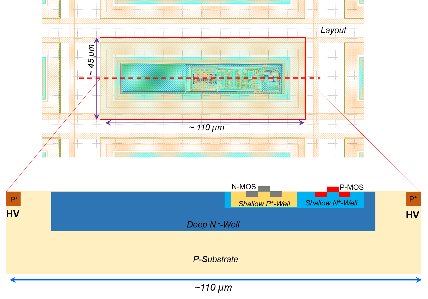
The ATLASPix2 is a fully monolithic HV-CMOS chip. Its design is similar to that of its predecessor, the ATLASPix1 chip [5, 6], with main differences being a smaller pixel matrix of pixels, several improved peripheral blocks (e.g. command decoder) and a single triggered readout scheme. Figure 1 shows the top layout and the schematic cross-section of a single ATLASPix2 pixel. The pixel active area is . A deep -well acts both as the charge collection electrode and as the substrate for PMOS transistors. Shallow and -wells, embedded in the deep -well, hold the analog electronics (charge amplifier and discriminator). A High-Voltage -implant placed outside the deep -well is used to deplete the -Substrate. The distance between the -well and the -implant has been carefully chosen using numerical TCAD simulations to achieve a breakdown greater than for non-irradiated devices [6]. The ATLASPix2 holds a single -implant guard-ring around the pixel matrix. The dicing edge to the guard-ring has been kept larger than .
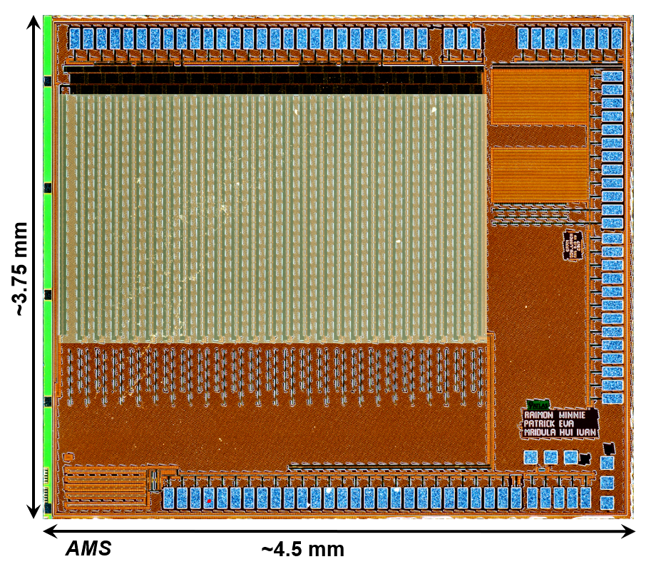
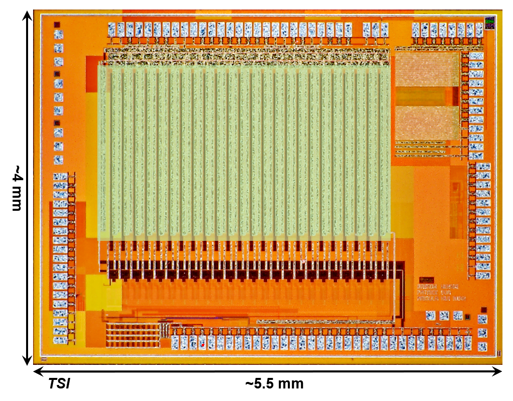
ATLASPix2 prototype chips have been fabricated at two different foundries, ams AG [3] and TSI Semiconductors [4]. Both batches were produced with P-type silicon substrate from the ingot TOPSIL [7]. In both cases, the wafers were of Magnetic Czochralski (MCz) crystal orientation, in diameter and standard substrate resistivity of 10-20 . No higher substrate resistivity has been explored. Figure 2 shows the micrograph of the two ATLASPix2 prototype chips. The diced reticle of the TSI prototype is slightly larger in size () in comparison to the ams one (). The 180 nm HV-CMOS process from TSI allows for one additional metal-layer in comparison to the ams technology, and therefore a few additional signal-pads for testing purposes have been integrated in the TSI chip. No differences in the electrical characteristics of the chips produced from the two foundries are expected from the inclusion of these additional test pads. After production, the wafers from ams AG (TSI) were thinned down to () by a Dicing Before Grinding (DBG) process.
3 Irradiation
Several ATLASPix2 chips (viz. Table 1) have been irradiated at the Jožef Stefan Institute (JSI) Neutron Irradiation facility at the TRIGA Mark II reactor [8]. In terms of neutron spectra and total flux values, the JSI TRIGA reactor has become a reference center for neutron irradiation of particle detectors. The pool-type reactor core has an annular configuration with a diameter of , 91 in-core positions for fuel elements and numerous irradiation positions. The samples were irradiated unbiased at the full reactor power () with a uniform neutron flux of , with an uncertainty of 10%. To reach the target cumulated fluences of , and , irradiation steps spanned few tens of minutes (e.g. 10.84 minutes for ). As soon as the extreme activation dropped to acceptable levels (typically 10 mins after irradiation), samples were stored in a fridge to avoid any annealing effect. While the ambient temperature at the reactor pool remained at , the temperature of the irradiated samples increased up to due to the high radiation backgrounds [9].
| Sensor ID | Foundry | Fluence |
| [] | ||
| AP2-AMS-08 | ams AG | |
| AP2-AMS-09 | ams AG | |
| AP2-TSI-05 | TSI | |
| AP2-TSI-11 | TSI | |
| AP2-TSI-06 | TSI | |
| AP2-TSI-24 | TSI | |
| AP2-TSI-08 | TSI | |
| AP2-TSI-17 | TSI |
4 Electrical characterization
4.1 Experimental setup
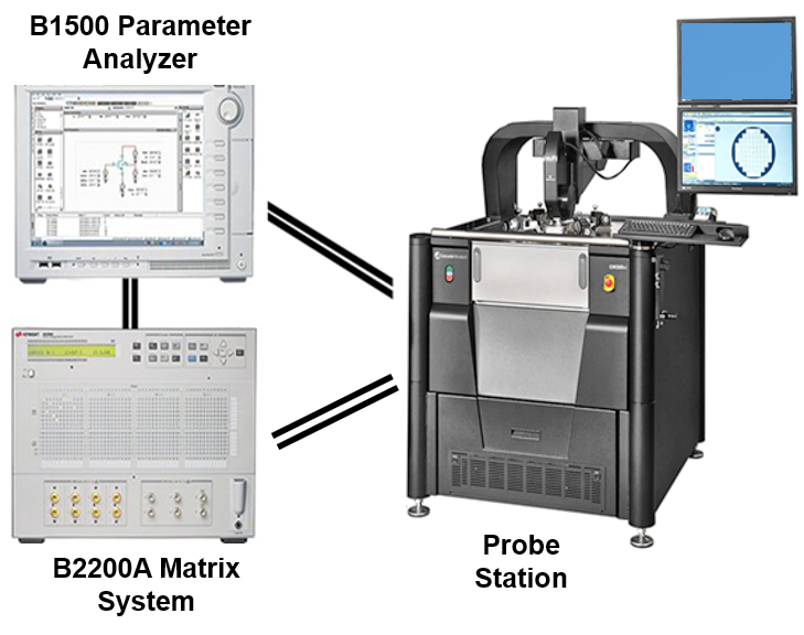
The electrical characterization of the different samples has been performed in the clean-room of the Department of Particle and Nuclear Physics (DPNC) of the University of Geneva with a Cascade Microtech CM300 semi-automatic probe station [10]. This system provides high attenuation ( dB) for precise low leakage current measurements and allows temperature probing in the range between and . The chuck used to hold the dies is a Nickel-coated Aluminum plate with a planarity of . Figure 3a shows the main components of the setup. In addition to the probe-station itself, a parametric analyzer (model Keysight B1500) and a logical switching matrix (model Keysight B2200A) are used. The Keysight B1500 can provide four Source Measure Unit (SMU) channels with an accuracy of each. For the I-V measurements, a Keysight B1510A High Power Unit provides a bias voltage accuracy of on the applied voltage range (). The accuracy of the current measurement depends on both the range of the current and of the applied voltage, but the uncertainity of measured data is only for a nonirradiated device. For the results presented in this paper, the reverse bias voltage was typically swept between 0 and 120 V.
The Capacitance-Voltage (C-V) measurements have been performed using a Multi-Frequency Capacitance Measurement Unit (MFCMU). Since the MFCMU has a DC bias range limited to , a separate SMU was used for higher-range voltage sweeps with additional decoupling capacitors. All C-V data have been acquired at with a input AC-signal. The total uncertainty of the C-V measurements includes the measuring instrument uncertainty, the discrete component’s tolerances (used in the decoupling box) and the fitting errors to the C-V curves. This total uncertainty is estimated to be of the reported values.
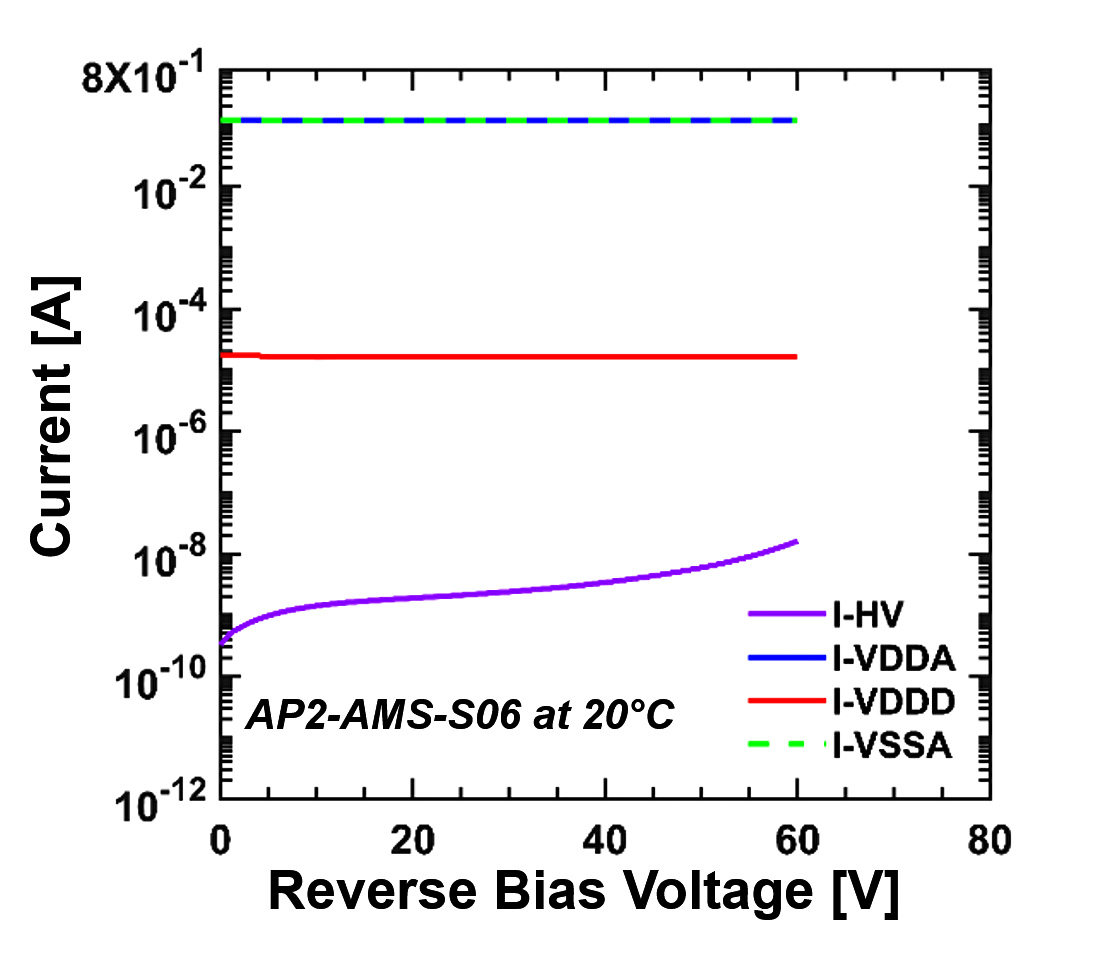
During the I-V measurements, all power lines of the readout electronics have been kept at their nominal values: for the digital (VDDD) and analog (VDDA) voltage supply, and for the analog front-end ground (VSSA). Figure 3b shows all different measured currents for a qualified ATLASPix2 prototype.
4.2 Definition of breakdown voltage
From the I-V characteristics, the breakdown voltage is determined as the maximum bias voltage for which , with the adimensional function being defined as
| (4.1) |
where is the sensor reverse current, is the applied bias voltage and is the slope of the measured I–V curve. This definition is independent of the depletion voltage and especially suitable for cases, where the leakage current shows a smooth and continuous rise due to defects existing in the original wafer or introduced in the silicon lattice after irradiation [11]. A -value less than 1 corresponds to the ohmic state of the sensor before breakdown. The case represents a real avalanche characteristics. In this paper, a -value equal to 4 has been chosen for the breakdown [12]. The error associated to the resulting breakdown voltage () is determined from the accuracy of the applied voltage and of the current sensing. Given the very high accuracy of current measurements in the range of interest, uncertainties in the breakdown voltage were mainly driven by the step chosen for the voltage ramp, which goes up to 2 V. The worst-case value () has been taken as an upper limit of for all measurements.
5 Results
5.1 Results before irradiation
As previously reported in [6], at near room temperature, the breakdown voltage for the ams ATLASPix2 was found to be , and for the TSI ATLASPix2 version. The ATLASPix2 version produced by TSI shows a breakdown voltage in good agreement with the numerical TCAD simulation, estimated to be . Selected samples of table 1 were probed by varying the chuck temperature between and with a step of and between to with a step of . The acquired leakage current data at different temperatures were then compared with the Shockley Read-Hall (SRH) model prediction at a reference temperature, using formula 5.1,
| (5.1) |
where is the reference leakage at as in [6], the Si band gap () [13] and the Boltzmann constant. The SRH model is the simplest approach to the modeling of the device leakage current as function of temperature, considering only the bulk generated current from carrier generation and recombination. Any disagreement between the measurements and the SRH prediction hints that leakage current from other sources than the bulk, such as surface leakage from the oxide-silicon interface due to stress, are present in the device.
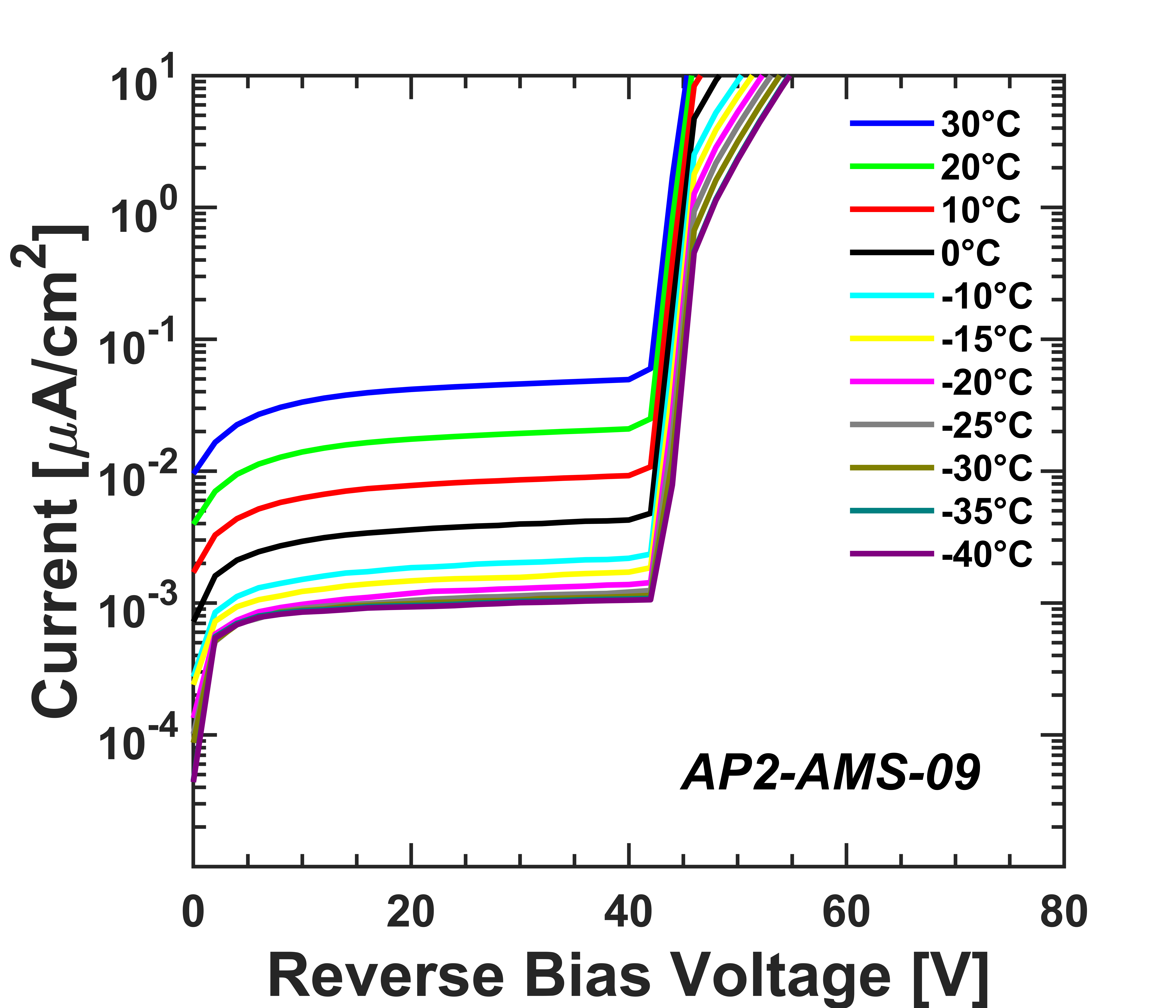
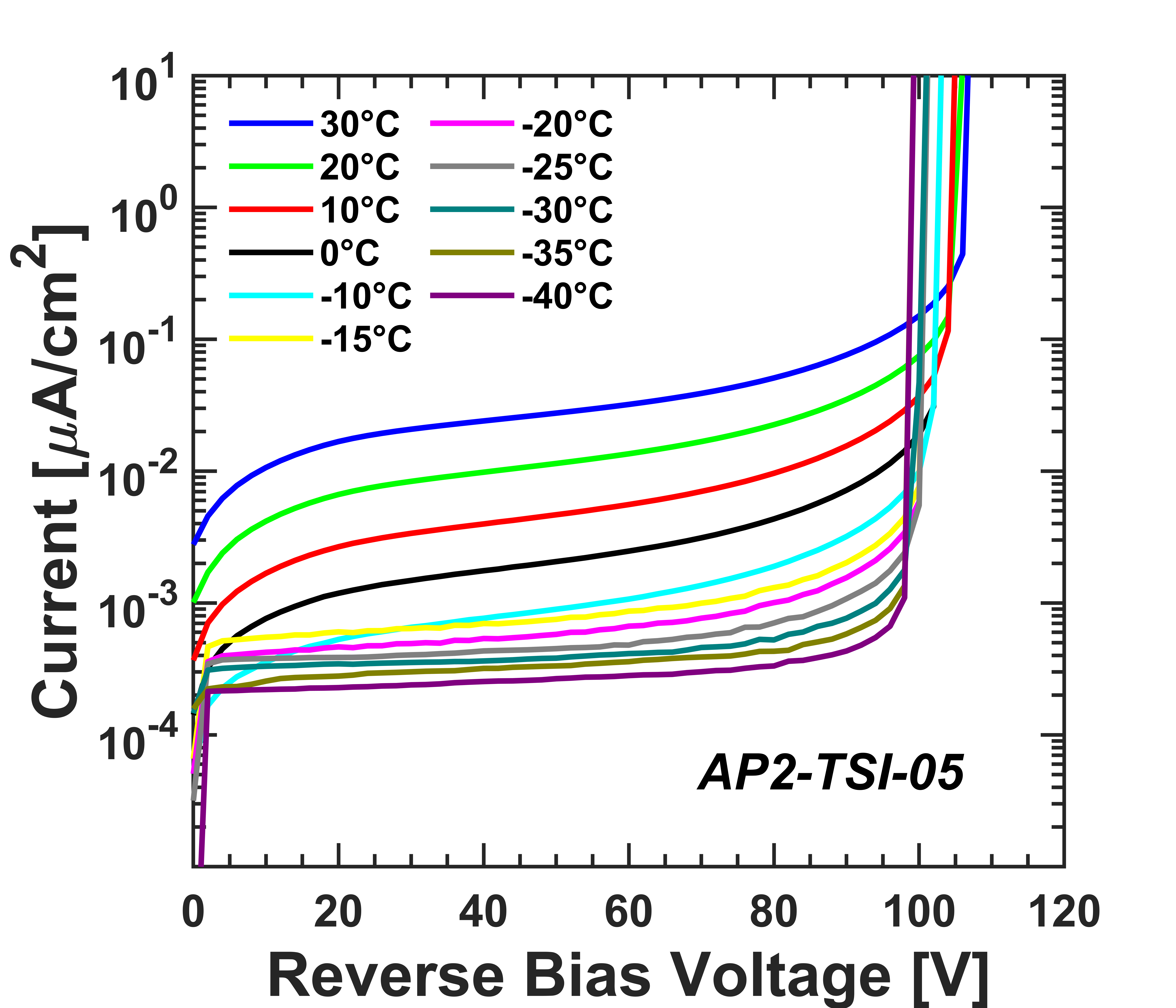
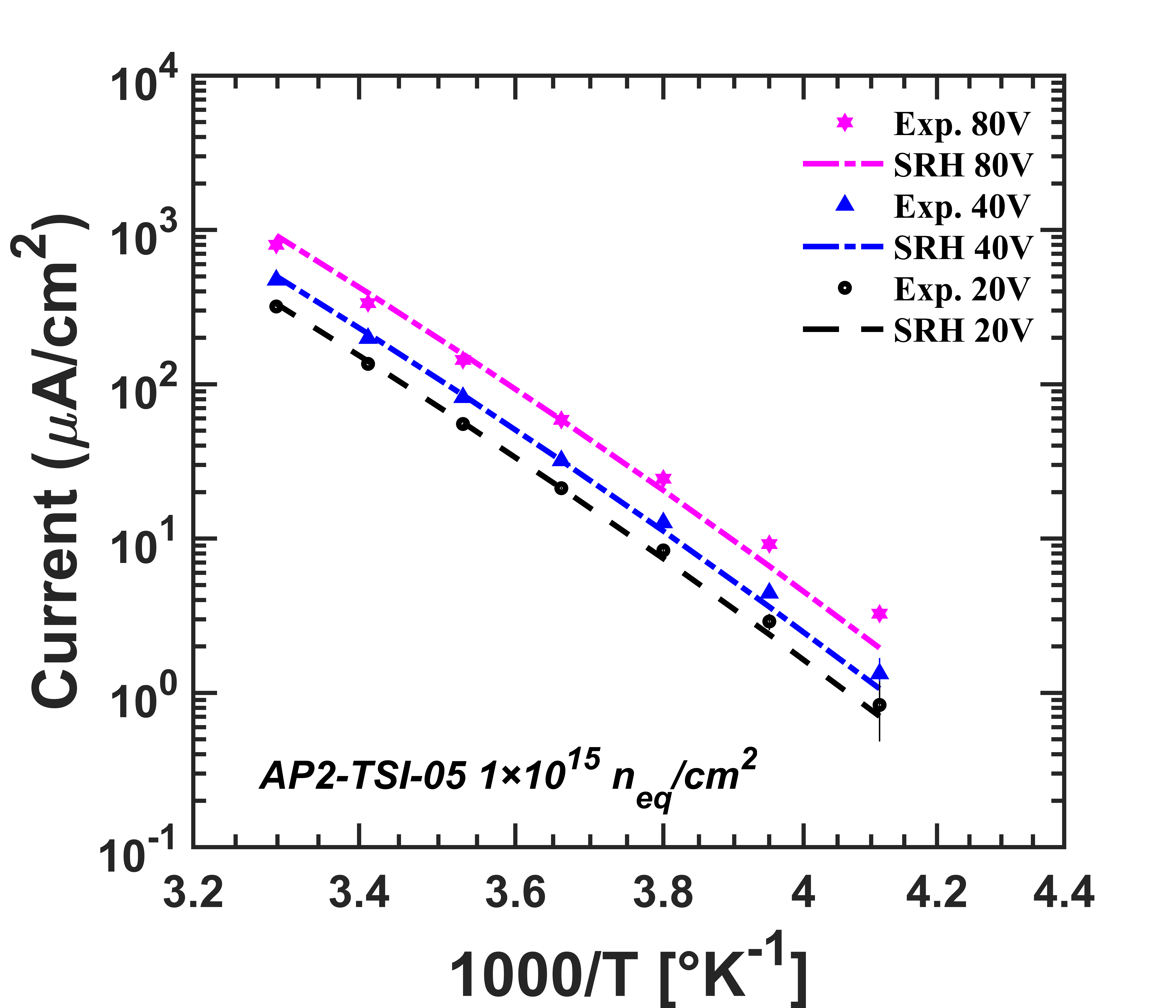
Figure 4 shows the I-V curves measured for both ams ATLASPix2 and TSI ATLASPix2. As expected, the leakage current decreases with a lower temperature. ATLASPix2 chips from ams production show a breakdown voltage of , similar to the earlier of HV-CMOS sensors, the ams ATLASPix1. Such an early breakdown in comparison to TCAD results could be the result of a large process-induced surface damage present only in the ams chip. Measured data have been fitted with the SRH model, using the reference temperature (equation 5.1). Careful observation in figure 4c shows little deviation from the SRH prediction at higher temperatures, and supports the hypothesis that for the ams sample, surface damage is adding an extra leakage current contribution. Figure 4b shows the current-voltage (I-V) characteristics of TSI processed samples. While the leakage followed the decreasing trend with lower temperature, the sensor breakdown voltage remained at around 100 V, as it was seen in [6]. It is worth noting that the breakdown voltage is reduced at lower temperature due to an increased ionization rate [14].
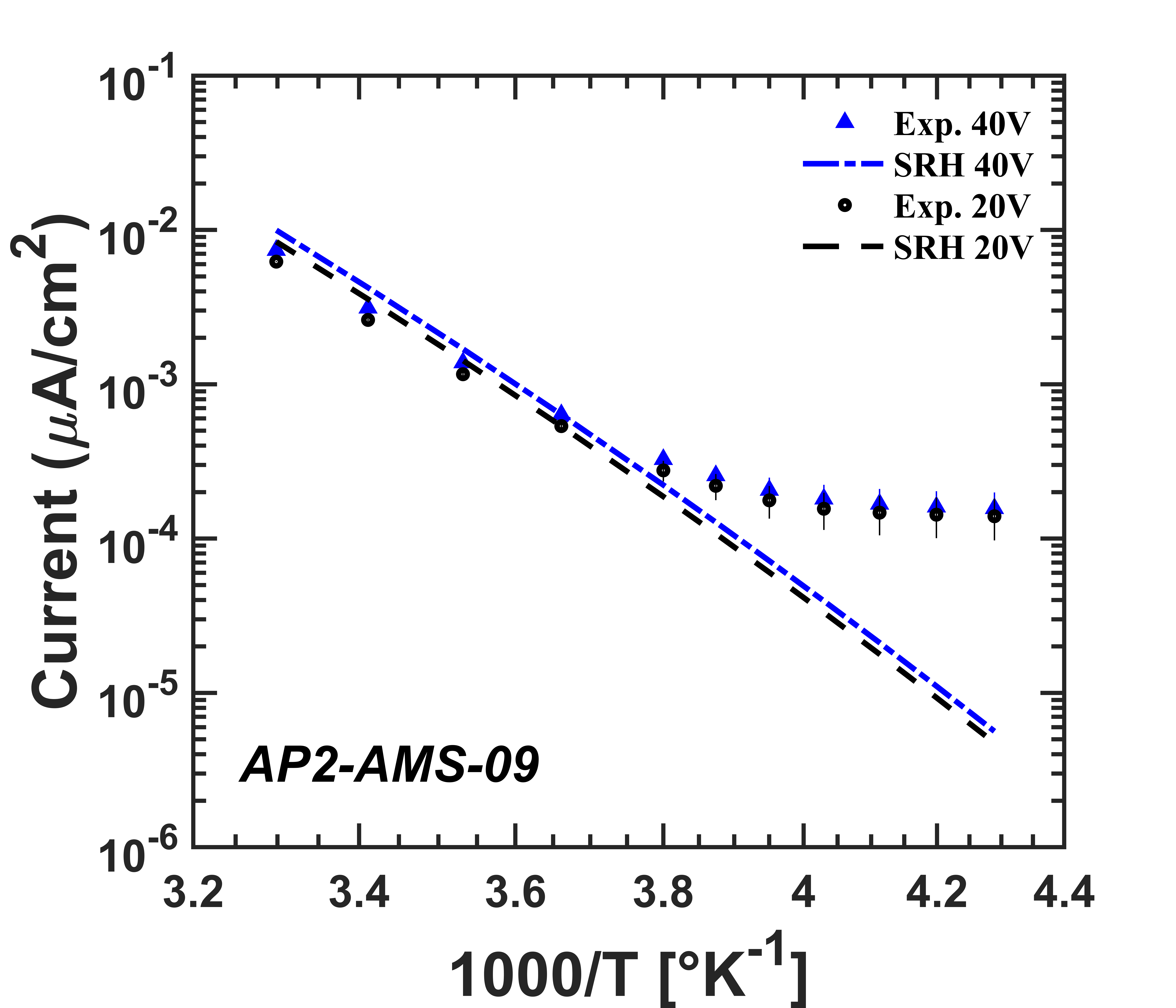
The leakage current of the TSI samples was found to be 6-7 times smaller than for the ams ATLASPix2. Arrhenius plot of the TSI sample (as found in figure 4d) shows a better agreement between measured leakage current and the SRH prediction even for a bias voltage reference a few volts before breakdown until . At temperatures lower than , the measured data clearly deviated from the SRH predictions, and the same phenomenon is also observed for the ams samples. At lower ambient condition, the mean free path of charge carriers increases and triggers earlier the impact ionization process. Therefore, there has been an early avalanche-introduced breakdown voltage for TSI ATLASPix2 prototypes at lower temperatures.
5.2 Results after irradiation
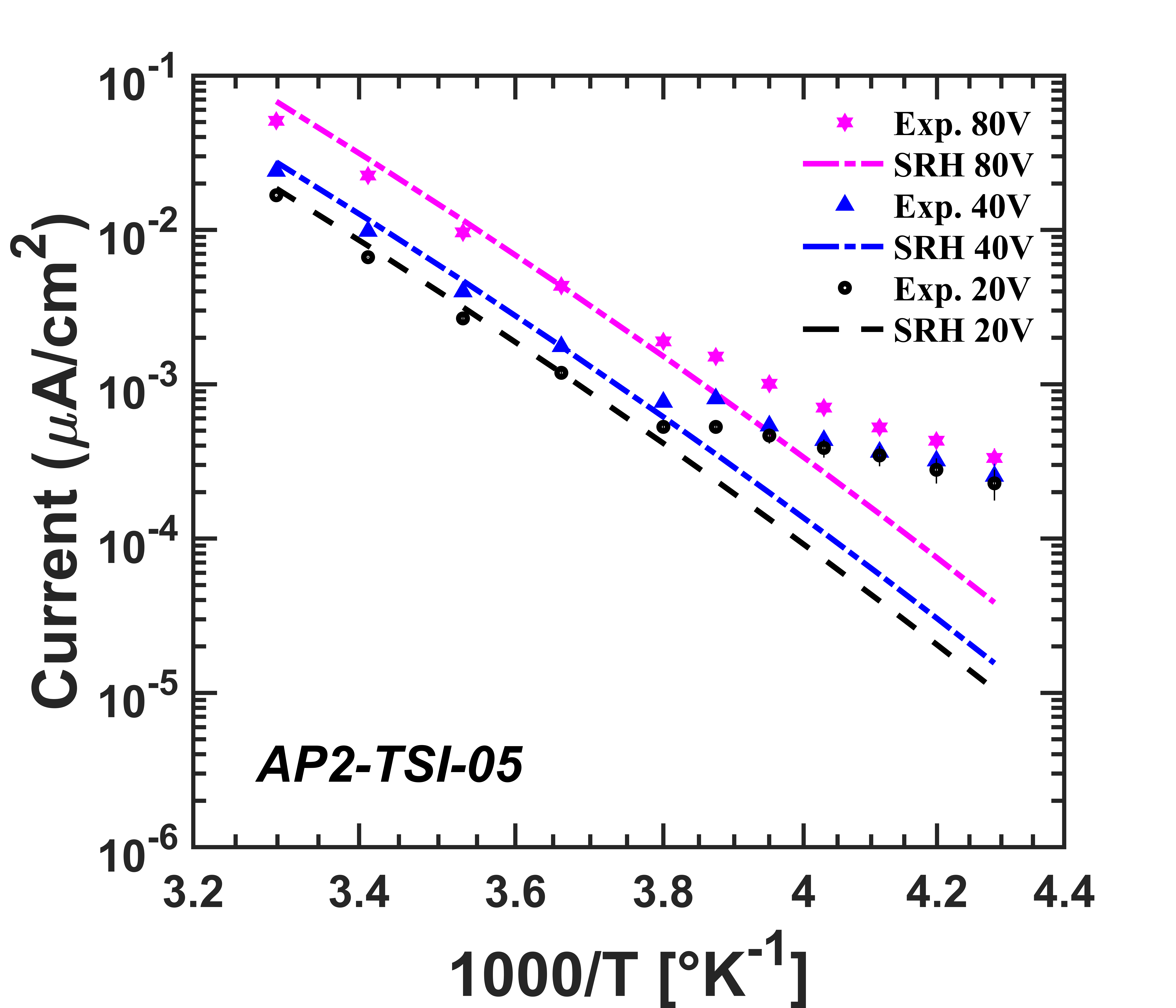
All eight ATLASPix2 samples from table 1 were sent for neutron irradiation to JSI and were then measured in the clean room facility of the DPNC - University of Geneva under controlled ambient conditions. As an example, figure 5 shows I-V curves for two prototypes of ATLASPix2 fabricated in ams (AP2-AMS-09), and TSI (AP2-TSI-05), and irradiated to . In both cases, the leakage increased by four orders of magnitude with respect to the data before irradiation. It can be explained by the introduction of electrically active traps, generated by crystalline defects produced by neutrons [12, 18, 15] and the surface damage increase due to background -rays, present at the JSI beam-line [8]. For irradiated ams chips, a breakdown voltage beyond is observed, slightly higher in comparison to the non-irradiated case. This can be explained by interface states (introduced by irradiation) fill up with carriers, where an additional reverse bias voltage is required to de-trap them before reaching the surface condition similar to a non-irradiated chip and triggering a delayed avalanche breakdown. On the contrary, the breakdown voltage of the TSI samples is measured to be , lower than a non-irradiated case. Before irradiation the TSI chip has already shown a comparatively smaller leakage current than an ams prototype, hinting to fewer surface interface traps from the production phase (a better surface condition). Despite the irradiation-related uncertainties (fluence, self-heating), it is expected that the TSI samples would still have a lower number of interface states in comparison to the ams samples after irradiation. These comparatively fewer active interface-states would have led TSI chips to experience a lesser fill-up of carriers. Thus, a larger peripheral and bulk charge-carriers may cause an earlier avalanche breakdown, where they drive into a device high electric field area near deep -well and P-substrate (viz. figure 1).
After irradiation, the predictions from the Arrhenius model have been compared again with the measured leakage current of both irradiated ams and TSI samples (figure 5c and 5d). Interestingly, samples from both foundries show a good agreement for all measured temperatures, meaning the leakage current increase after irradiation is mostly driven by thermionic emission process in the bulk of the sensors.
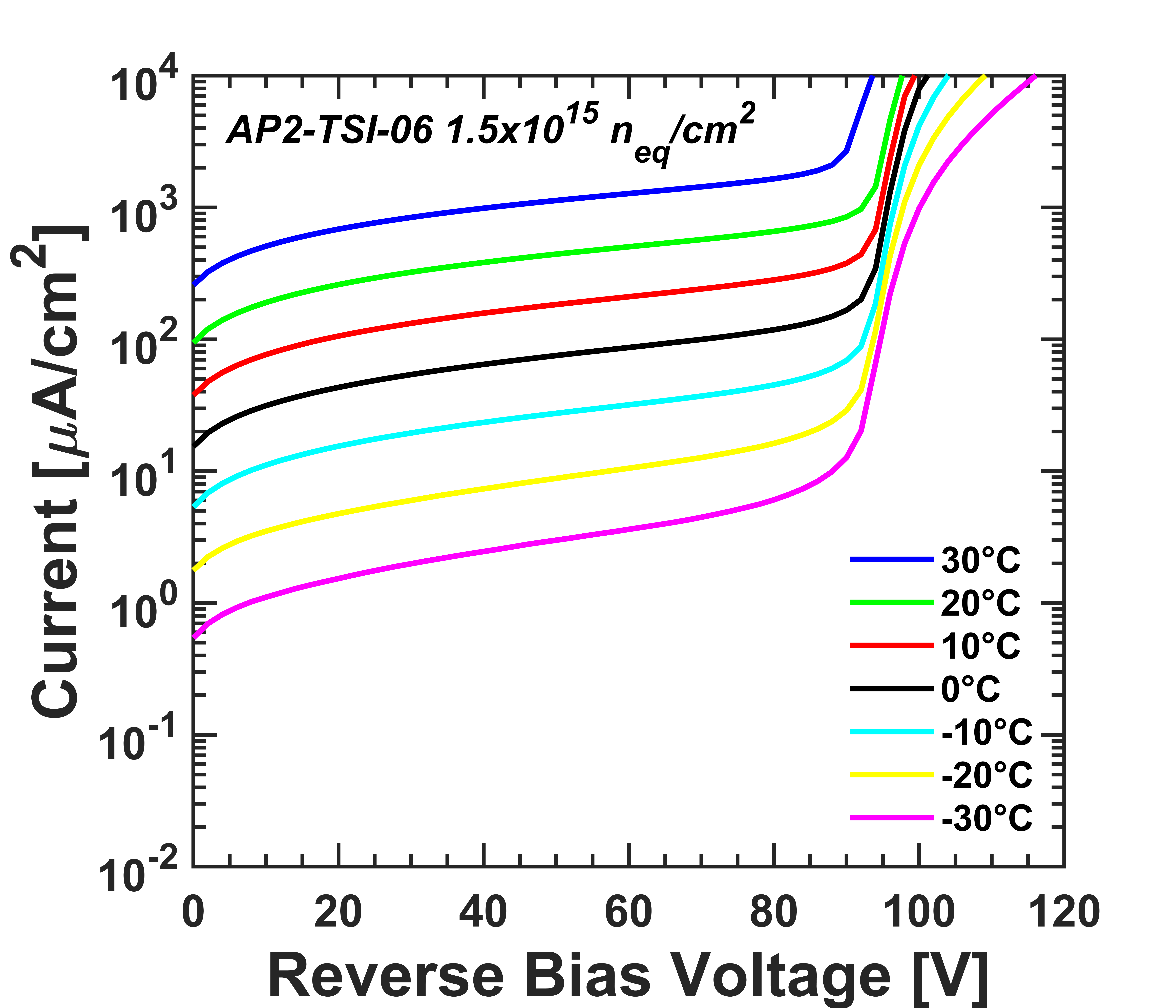
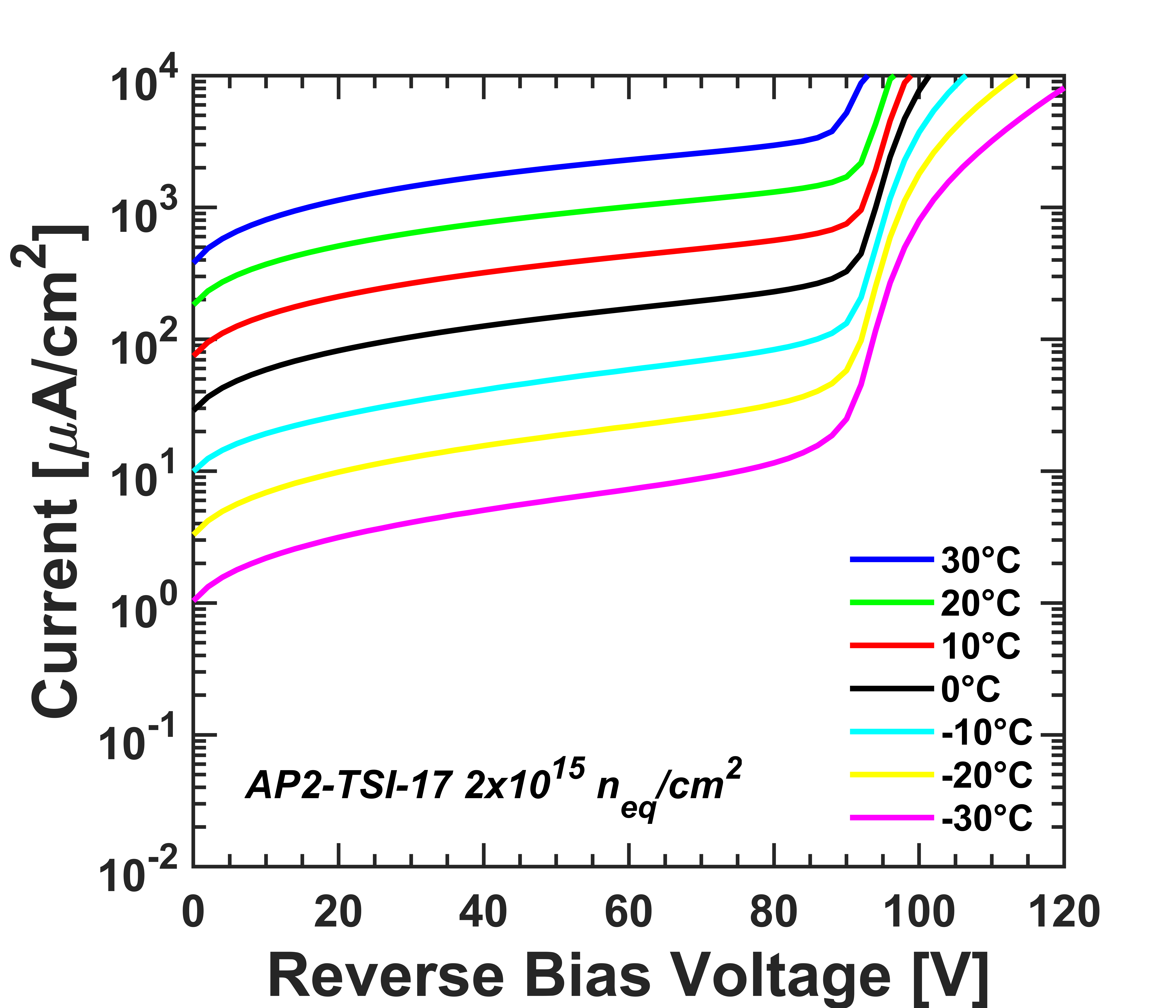
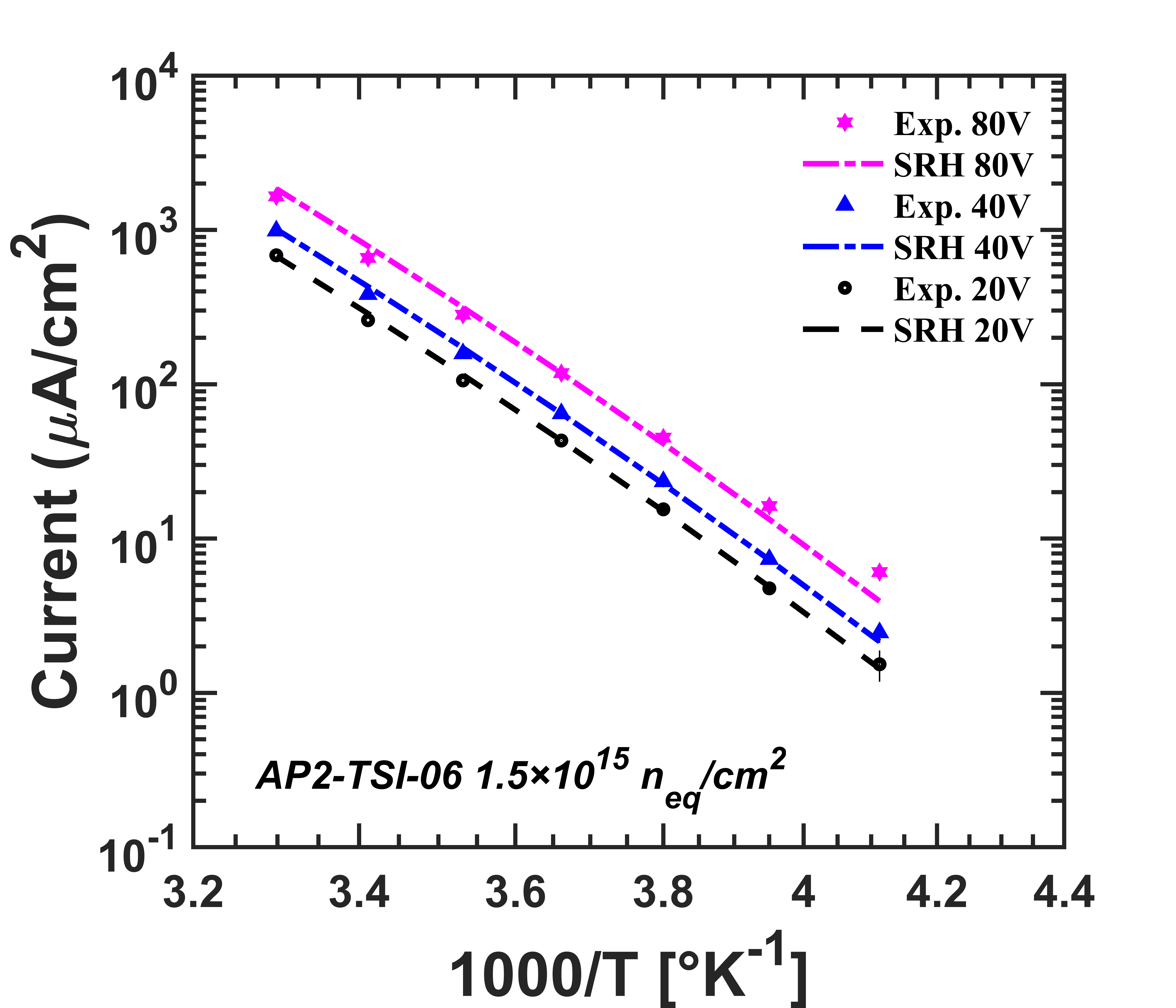
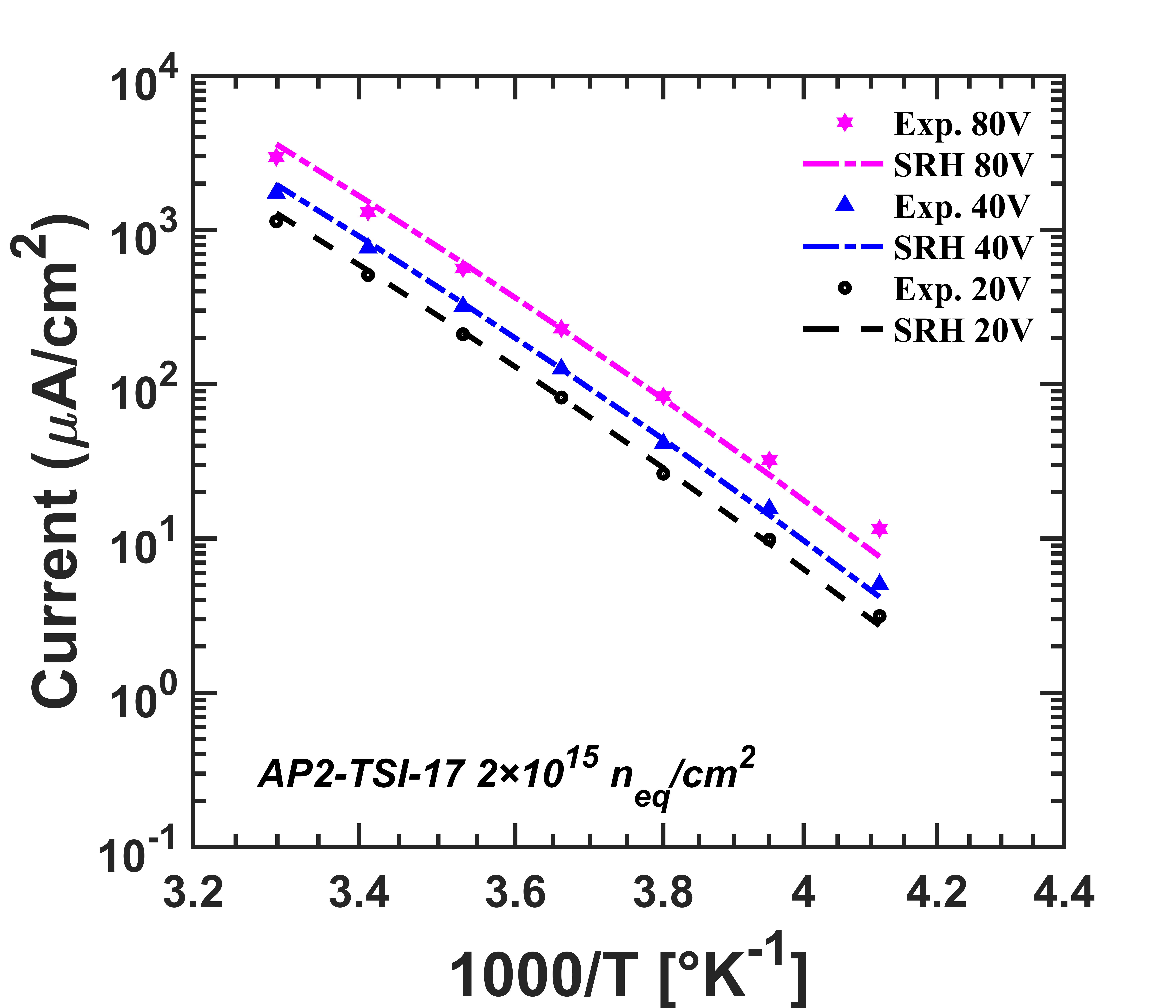
Figure 6a and 6b show the I-V measurements of the TSI processed samples irradiated to and neutrons at JSI. The breakdown voltage is reduced by a few volts () with regard to the TSI samples irradiated to neutrons. More interface states are formed with higher irradiation fluences (by -rays) and therefore leads to an early avalanche breakdown. The leakage current of the TSI sample increases by a factor of and respectively, regarding the non-irradiated case compared to the irradiated cases with and neutrons. A clear agreement between the Arrhenius model and the measured leakage data at different temperatures (as seen in figure 6c and 6d) is observed, again showing the bulk generated current remain dominant after irradiation.
| Fluence | TID | Device ID | |||
| [Mrad] | [] | [V] | |||
| 1.1 | AP2-AMS-08 | @64 V | @50V | ||
| AP2-AMS-09 | @66 V | @50V | |||
| AP2-TSI-05 | @88 V | @80V | |||
| AP2-TSI-11 | @88 V | @80V | |||
| 1.65 | AP2-TSI-06 | @86 V | @80V | ||
| AP2-TSI-24 | @88 V | @80V | |||
| 2.2 | AP2-TSI-08 | @86 V | @80V | ||
| AP2-TSI-17 | @86 V | @80V |
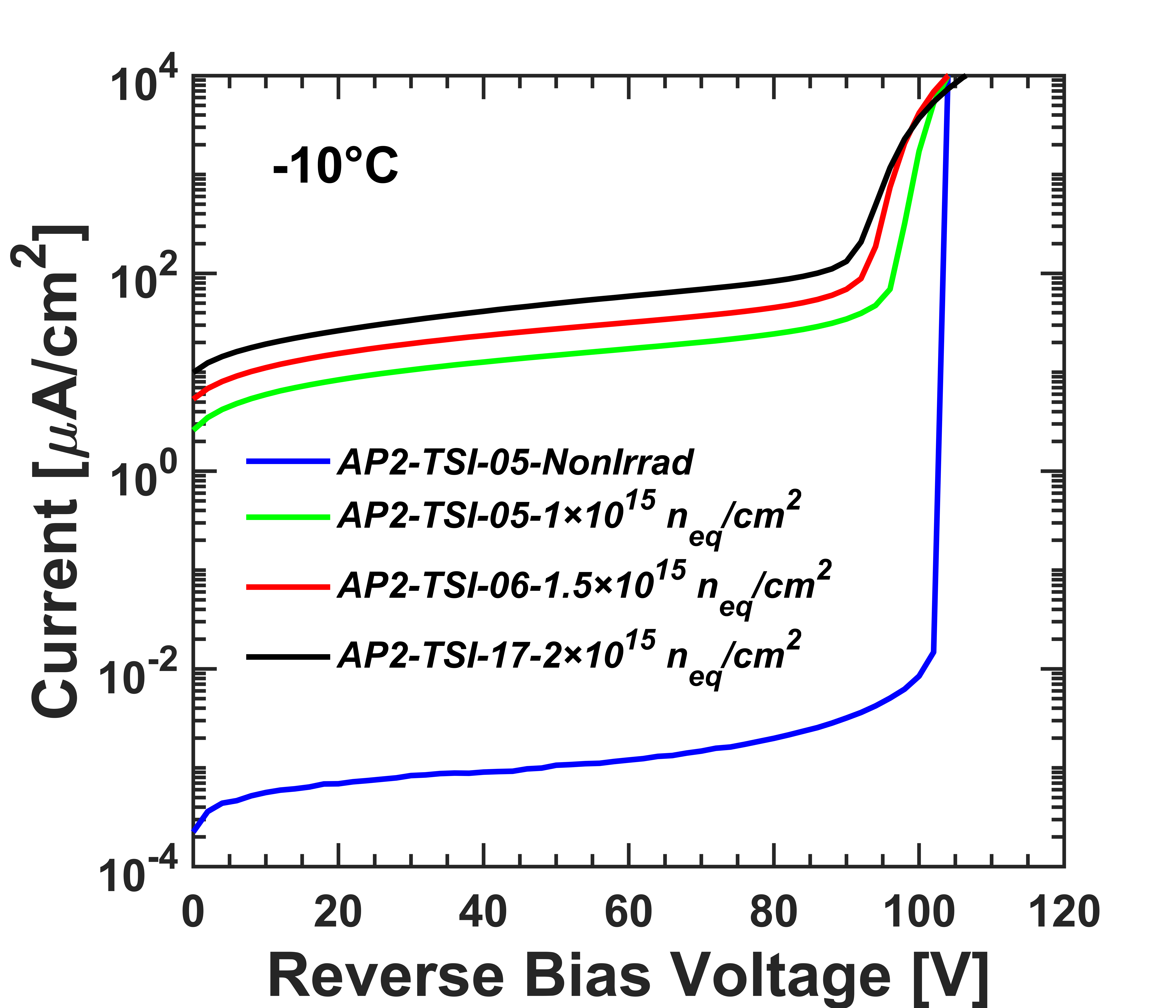
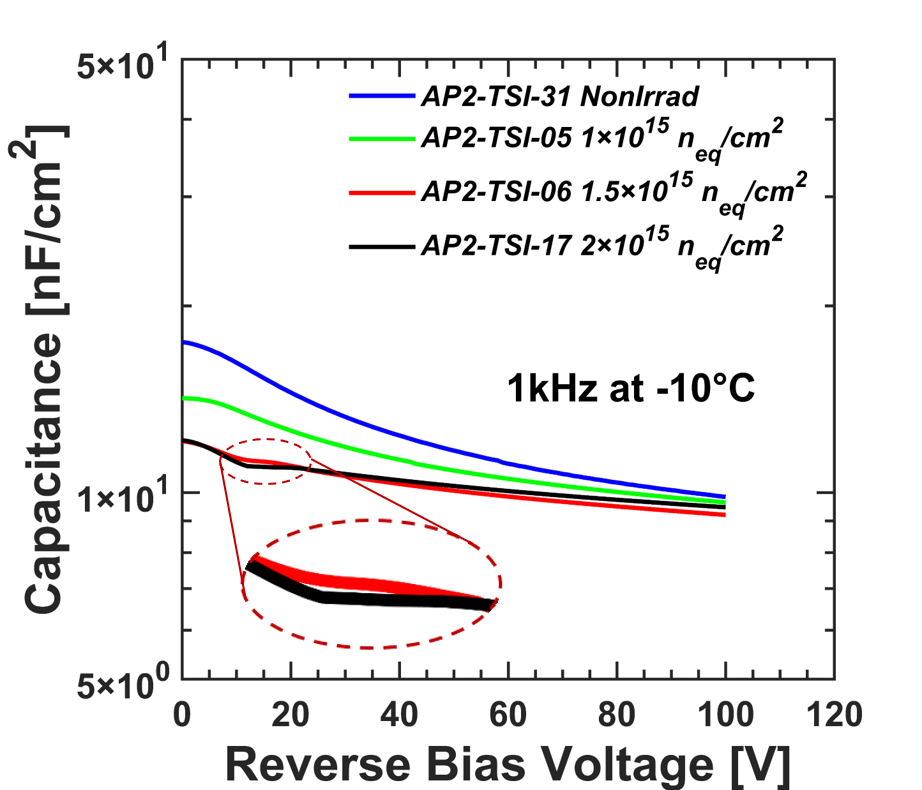
Table 2 summarizes the electrical characterization data of all irradiated samples. While the leakage current density () includes contributions from both the bulk and the peripheral current, the damage constant provides information about the irradiation effects in the active pixel volume. The damage constant , as defined in [20] to deal with highly irradiated sensors where full depletion cannot be achieved, is just dependent on the chip thickness. In our case the usage of is considered to be more appropriate than due to the absence of dedicated edge-TCT measurements for the estimation of the depletion depth (needed for the calculation of ). The values shown in Table 2 are in reasonable agreement with those observed in other irradiated devices not subject to a high temperature annealing process [20, 15].
Figure 7a shows the comparative I-V plots of the TSI ATLASPix2 sensors, irradiated at different accumulated fluences and measured in - steps. The leakage current increased with a higher fluence received. Again, the -rays present at JSI neutron beam increase the density of interface states. Bulk trap-density also increases with exposure to neutrons and modifies the effective doping concentrations. Consequently, as previously explained, a smaller avalanche-driven breakdown voltage was observed for samples exposed to higher fluences.
The introduction rate of traps is proportional to the received fluence and affects the substrate effective doping concentration and therefore the electric field distribution under bias, thus affecting the depletion voltage. In this context, C-V measurements were made for different TSI ATLASPix2 samples. Figure 7b comprises the measured C-V data for TSI samples, irradiated with different fluences. Because of the larger sensor thickness () in comparison to the expected depletion depths of tens of microns [6] for our samples, no plateau after full depletion can be observed. For higher neutron fluences ( and ), a sort of plateau observed in the reverse bias range that perhaps denotes the lateral depletion (figure 7b). Per-pixel capacitance is found to be approximately .
5.3 Annealing
It is foreseen that the installed detectors at the HL-LHC will experience annealing during the required periodic shutdowns. To understand the annealing-driven effects on these sensors, a systematic study by accelerated annealing was performed. From irradiation, interstitial and vacancy defects are typically formed within the sensor. During the annealing process, several kinds of recombination happen: Frenkel pair recombination, multi vacancy and multi interstitial combination and combination of more complex defects [15]. The first two types are typically very mobile and can be cured at room temperature in a short period. The recombination of complex defect rather requires a longer time and affects adversely the sensor’s leakage current, the depletion voltage, and Charge Collection Efficiency (CCE). The accelerated annealing process at an elevated temperature helps to mitigate vacancies and defects, acts as the beneficial annealing initially by reducing the leakage current and the depletion voltage. However, acceptor removal is also dependent on annealing time and temperature and may trigger the reverse effects, as detailed in [16, 17]. The damage constant rate, , can be corrected for room temperature annealing from accelerated annealing using the model proposed in [15],
| (5.2) |
where is evaluated at a time and annealing temperature , and is the initial annealing period, fixed to . The model consists of an exponential term related to bulk effect and a logarithmic term related to surface effects. The correction factor is used to quantify the damage constant rate below , and is computed from the following equation:
| (5.3) |
| [min] | ||||
|---|---|---|---|---|
| 21 | 1.23 | 7.07 | 3.29 | |
| 60 | 1.26 | 94 | 4.87 | 3.16 |
| 80 | 1.13 | 9 | 4.23 | 2.83 |
| Annealing stage | Temperature | Duration | Equivalent annealing at |
|---|---|---|---|
| 1st stage | 80 min | 18 days | |
| 2nd stage | 30 min | 53 days | |
| 3rd stage | 120 min | 288 days | |
| 4th stage | 300 min | 634 days |
An effective activation energy of for irradiated Si was used, following [13]. The temperature steps for the study were carefully chosen since it has been observed that MCz P-type substrate (used in our prototypes) experiences reverse annealing for an annealing treatment beyond [18]. The first annealing step was made at for for all irradiated samples of table 1 and in later steps, selected irradiated samples from the 1st stage annealing were further treated with accelerated annealing process at for , and successively. All necessary values of , , and time constant, for equation 5.2 were taken for the corresponding annealing temperature, as can be found in table 3. These values were selected because of a better agreement with years-long annealing data of silicon sensors at the LHC [19] than the recommended values proposed in [15]. The equivalent annealing time at near room temperature () from the applied accelerated annealing has been shown in table 4 by numerically solving the equations 5.2 and 5.3.
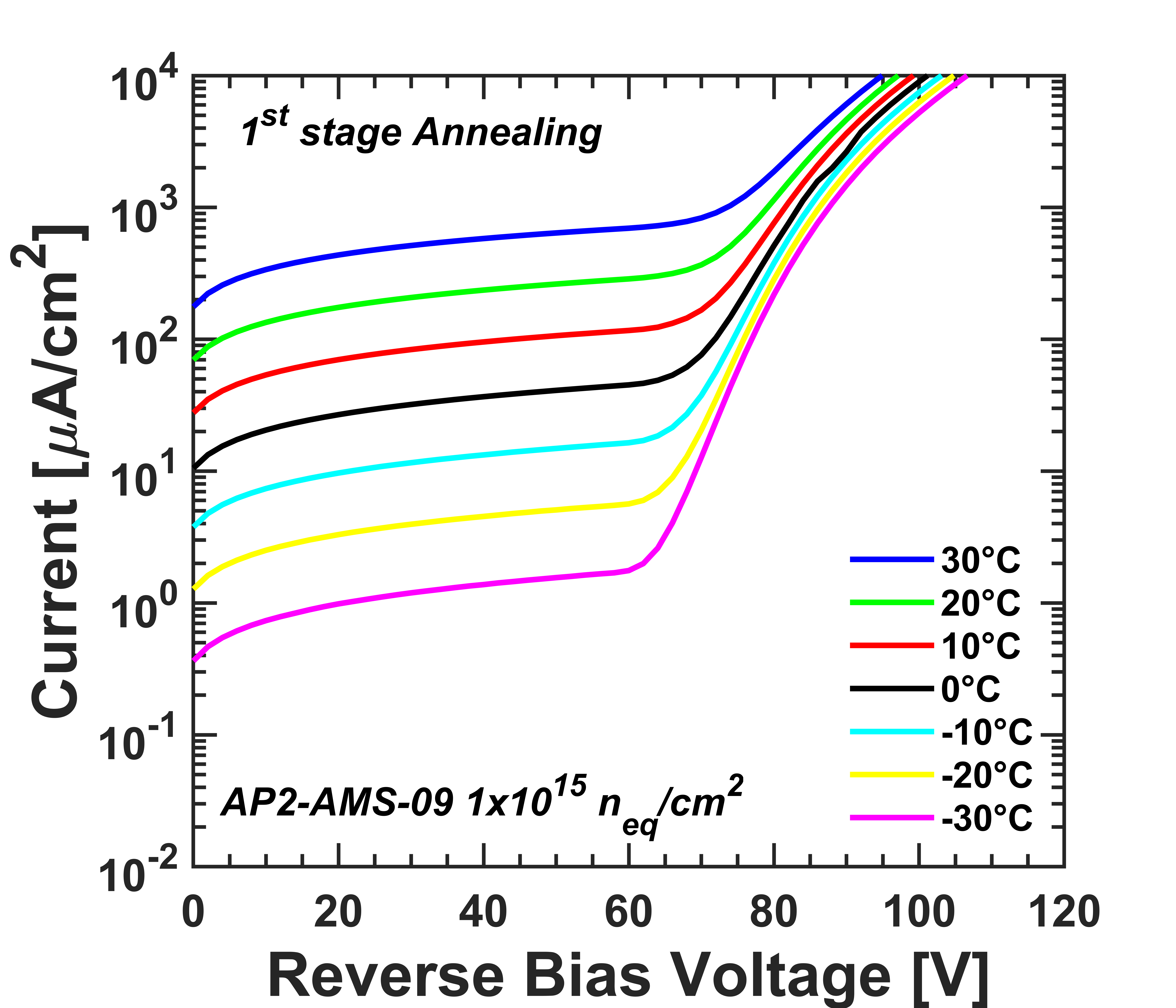
5.3.1 First stage annealing ( for 80 min)
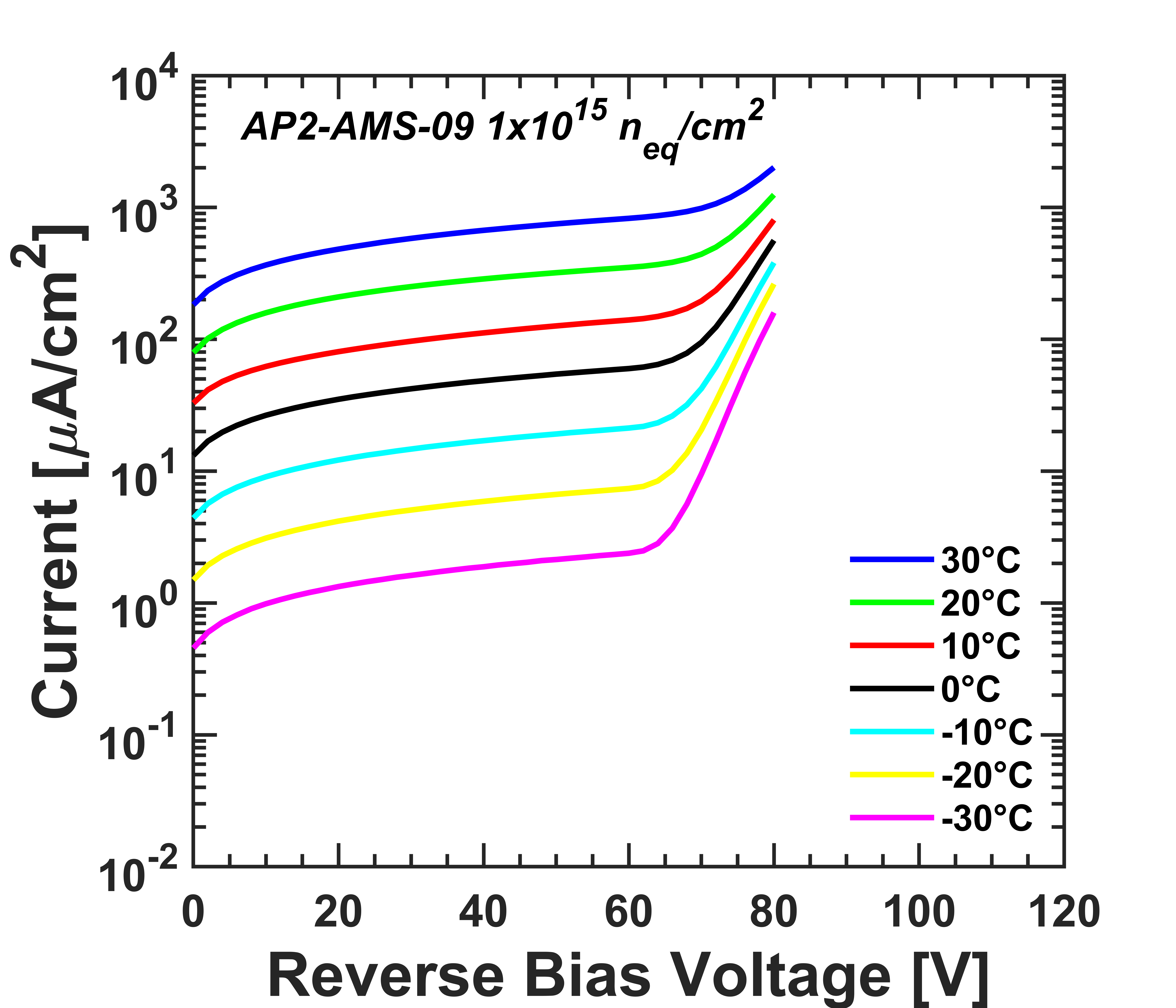
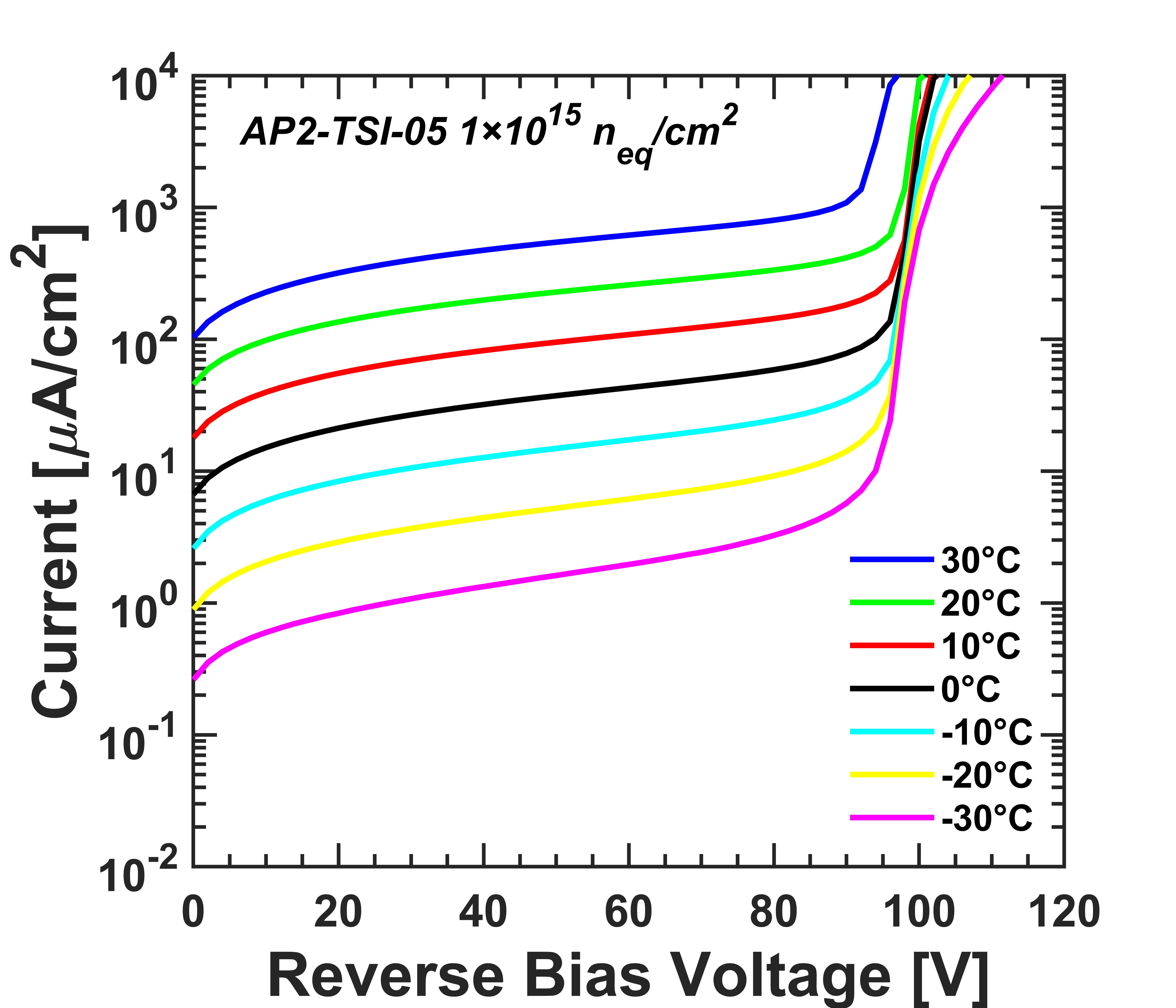
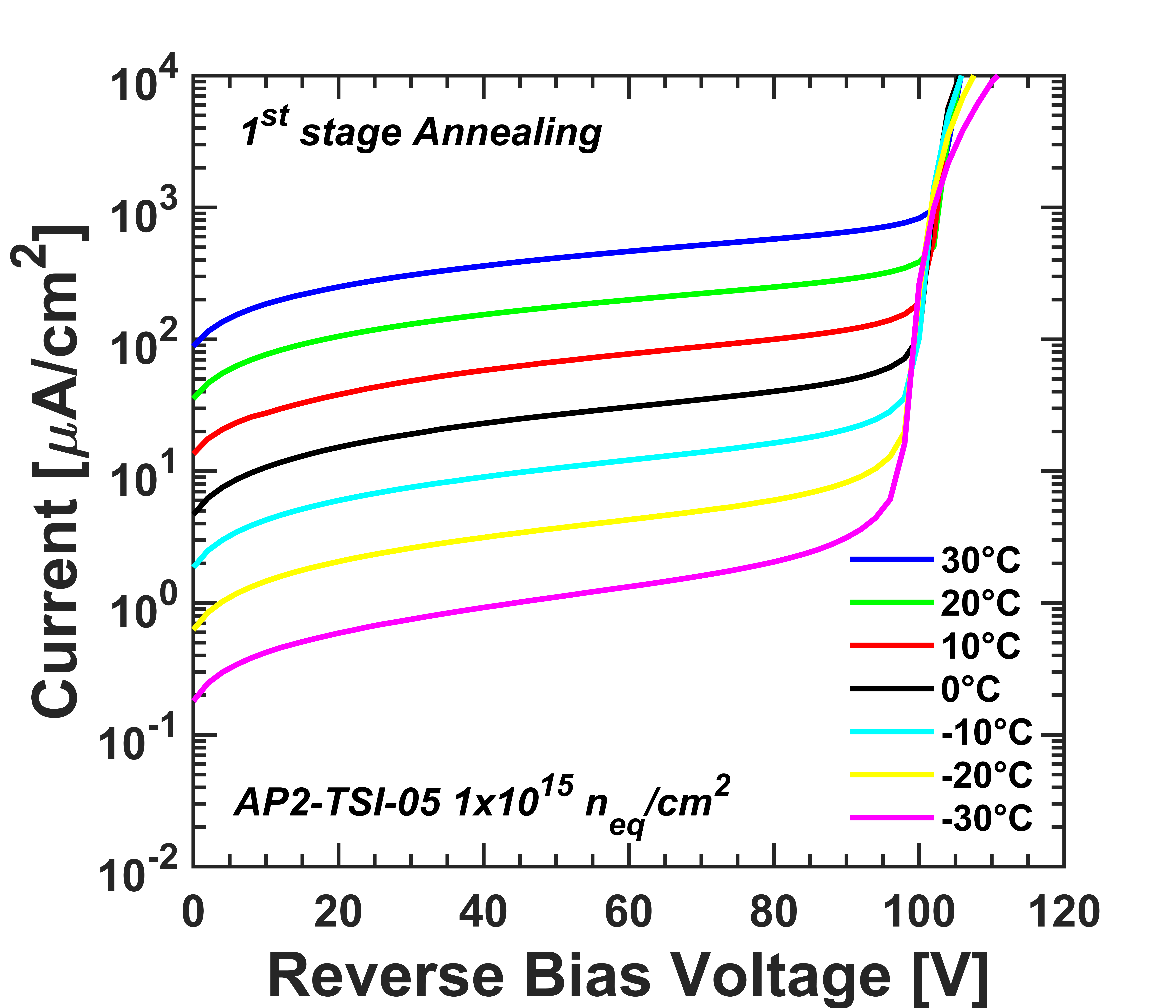
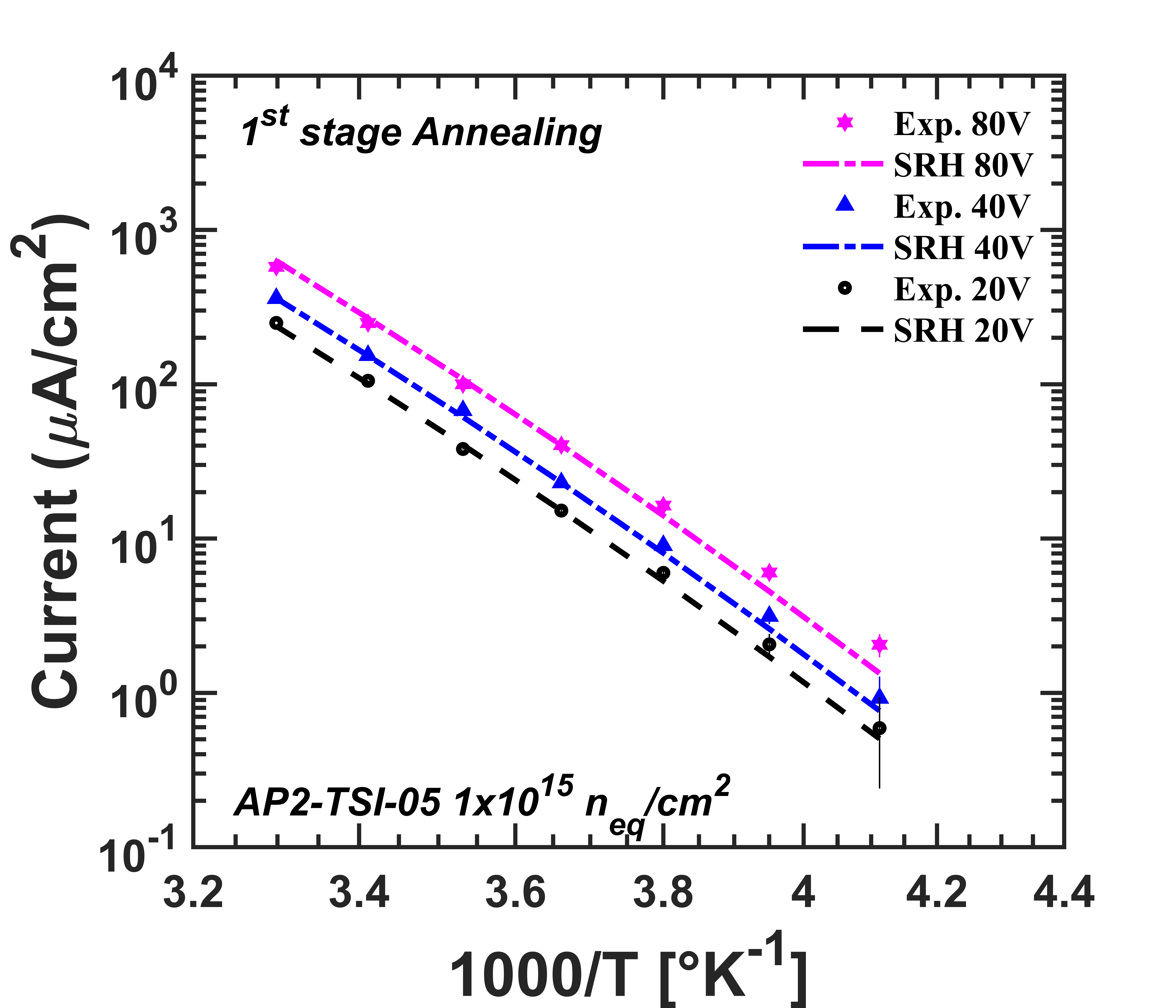
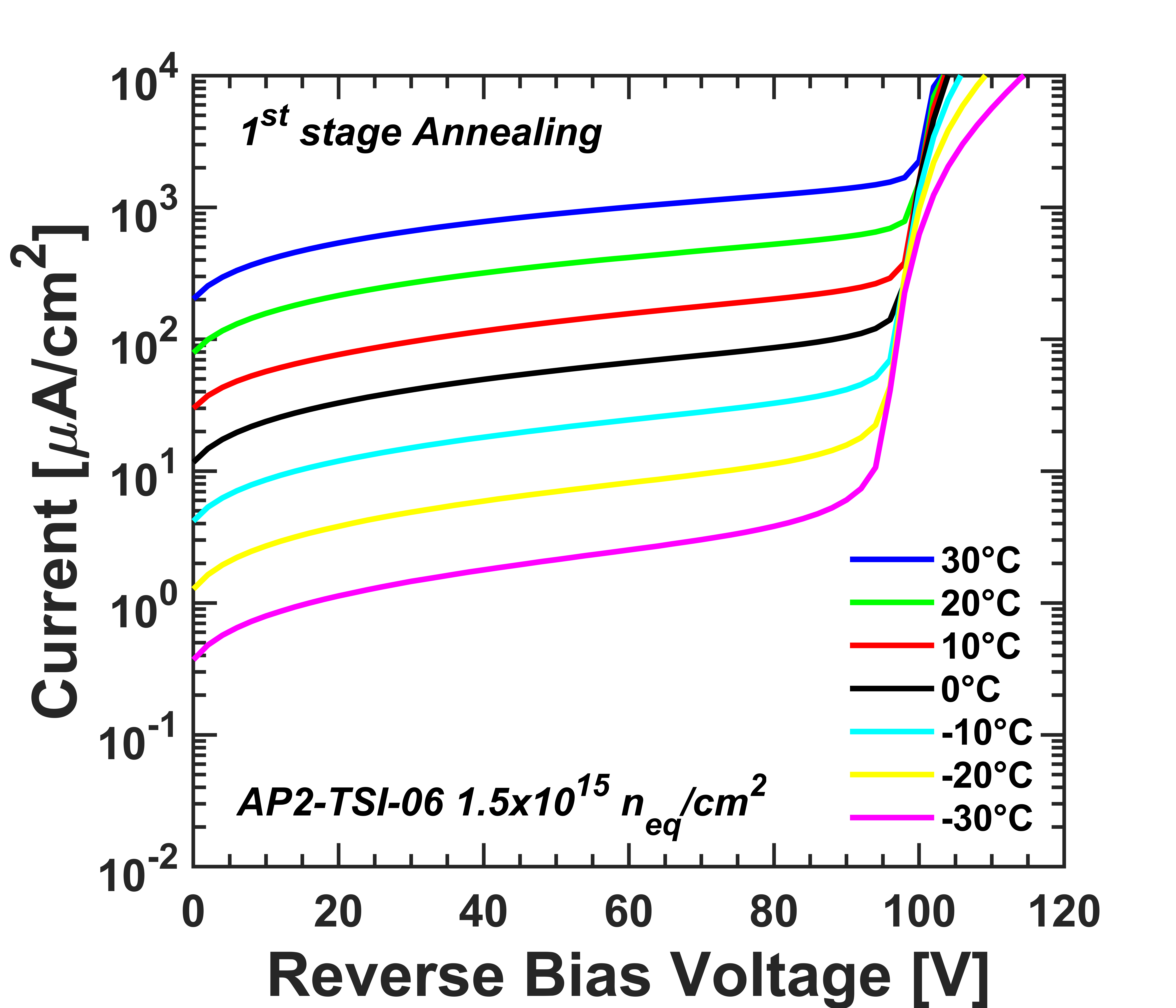
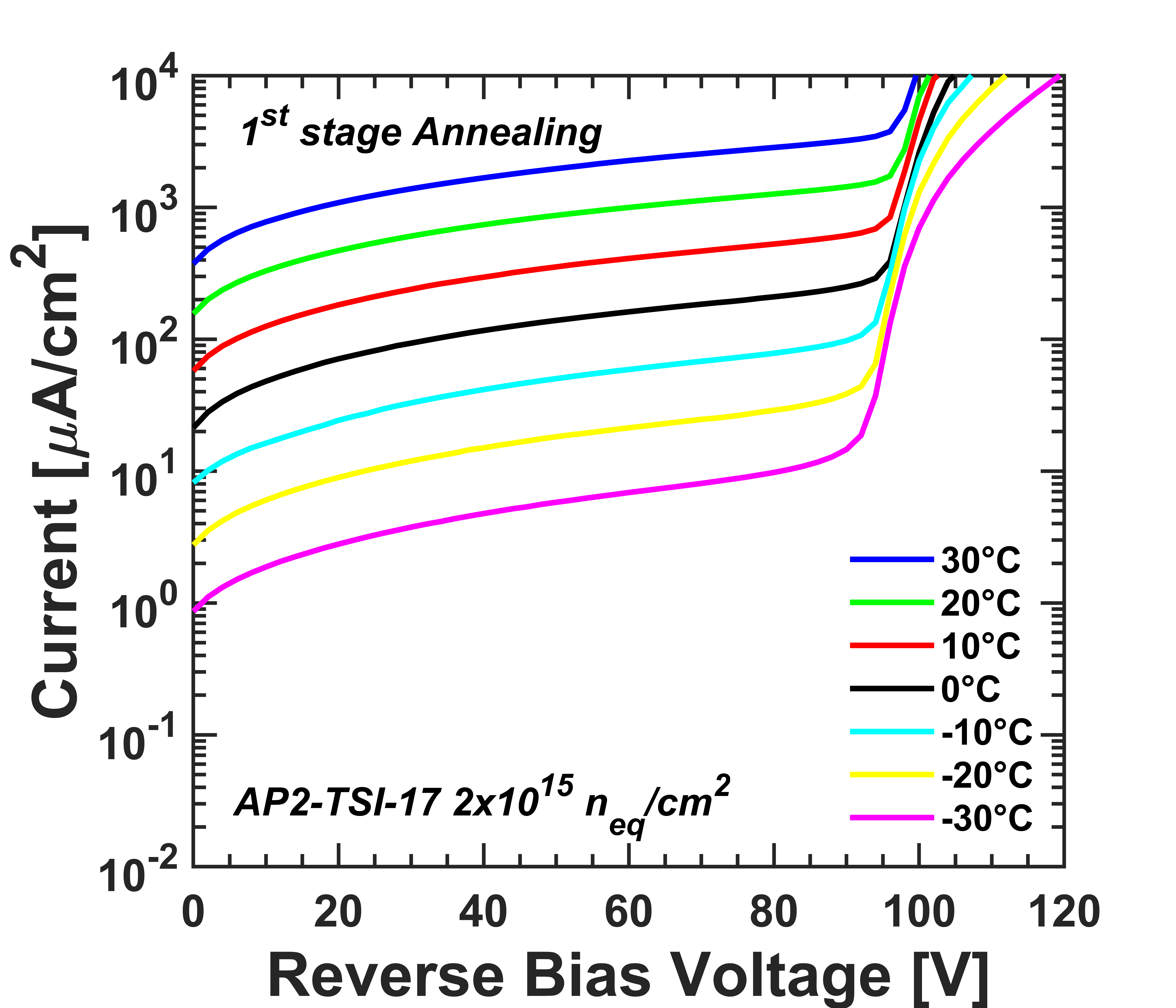
All the neutron-irradiated samples were annealed on the thermal chuck of CM300 at for 80 min in the first stage. Table 5 summarizes the data obtained from the I-V characterizations after annealing. Figure 8 shows the I-V behavior of ams (AP2-AMS-09) and TSI (AP2-TSI-05) prototypes irradiated up to neutrons and treated with first stage accelerated annealing. Interface states and traps recovery by accelerated annealing led to a leakage current decrease and a lower value of the damage constant rate is obtained. The interface states recovery and the effective doping concentration reduction by the first stage of accelerated annealing possibly helped to delay the avalanche process for TSI sample and improve the breakdown voltage by a few volts.
| Fluence | Device ID | Equiv. cum. | |||
| [] | [V] | ann. at | |||
| AP2-AMS-08 | @62 V | @50V | 18 days | ||
| AP2-AMS-09 | @64 V | @80V | |||
| AP2-TSI-05 | @92 V | @80V | |||
| AP2-TSI-11 | @92 V | @80V | |||
| AP2-TSI-06 | @92 V | @80V | |||
| AP2-TSI-24 | @92 V | @80V | |||
| AP2-TSI-08 | @92 V | @80V | |||
| AP2-TSI-17 | @90 V | @80V |
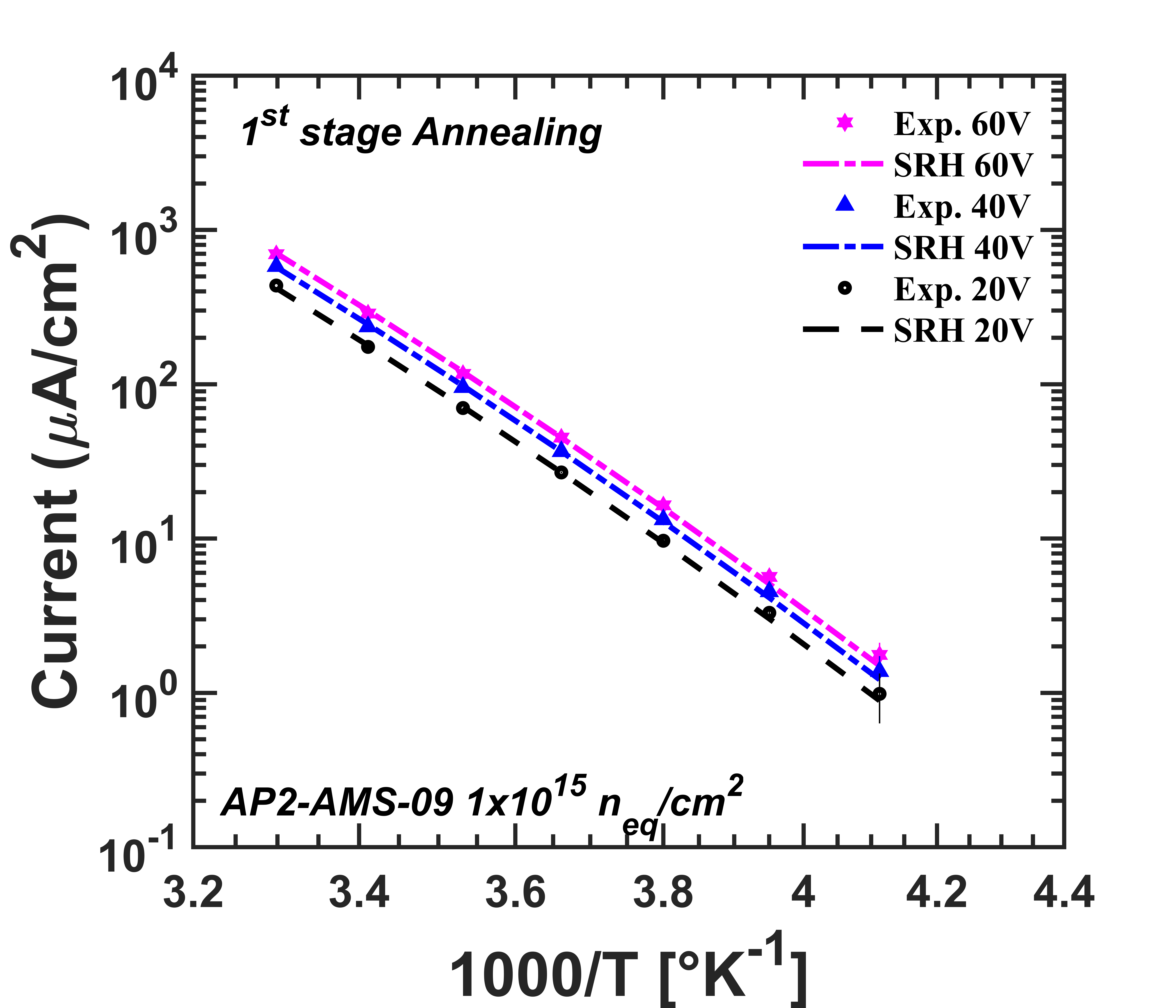
In contrast, the annealing treatment of the ams prototype enhanced the already present surface leakage by recovering the interface states. These carriers were triggering the ionization process at a relatively low reverse bias and so, the breakdown voltage of ams candidate is reduced by a few volts in comparison to data reported before annealing. The good agreement of measured data for annealed samples to the Arrhenius predictions is visible though in figure 8c and 8d.
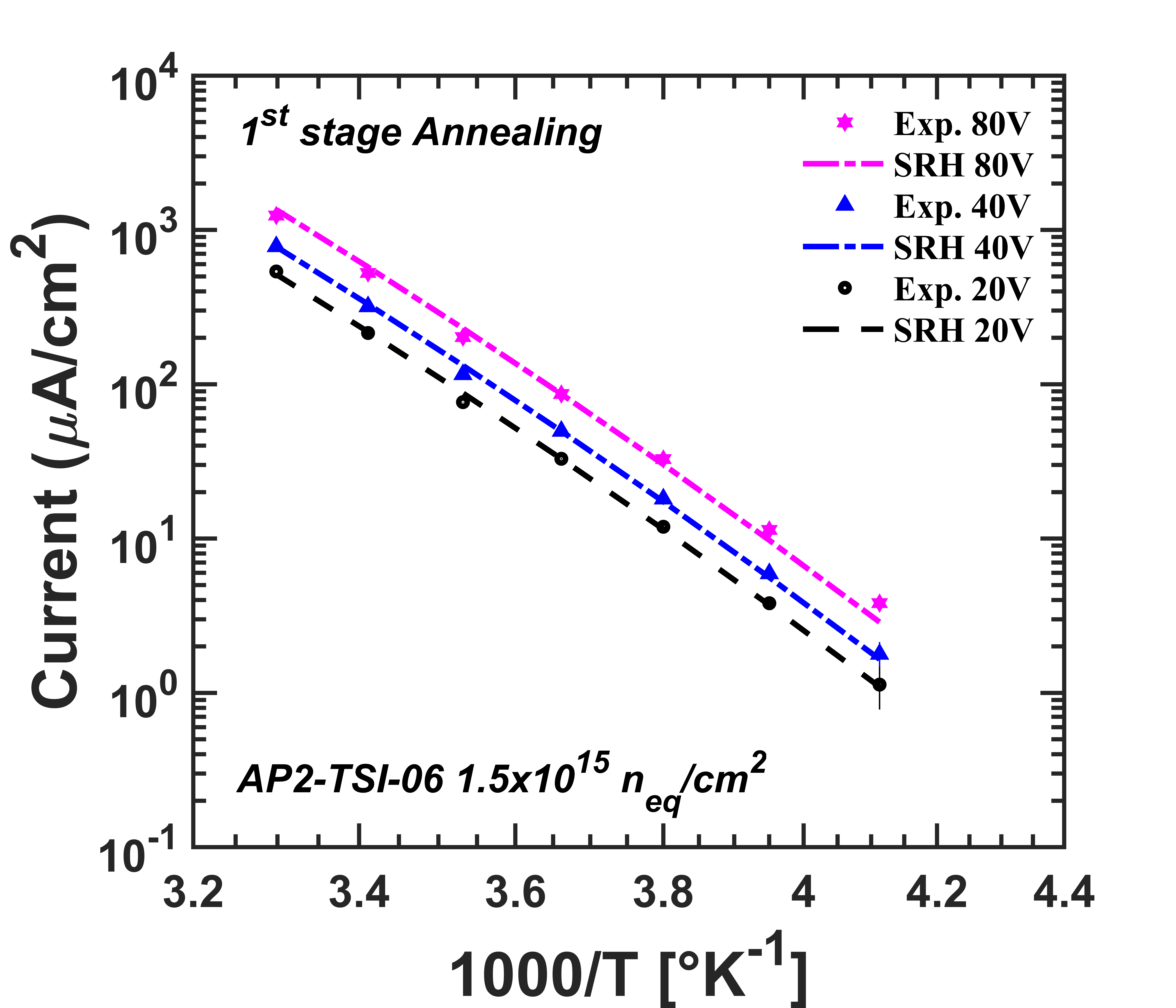
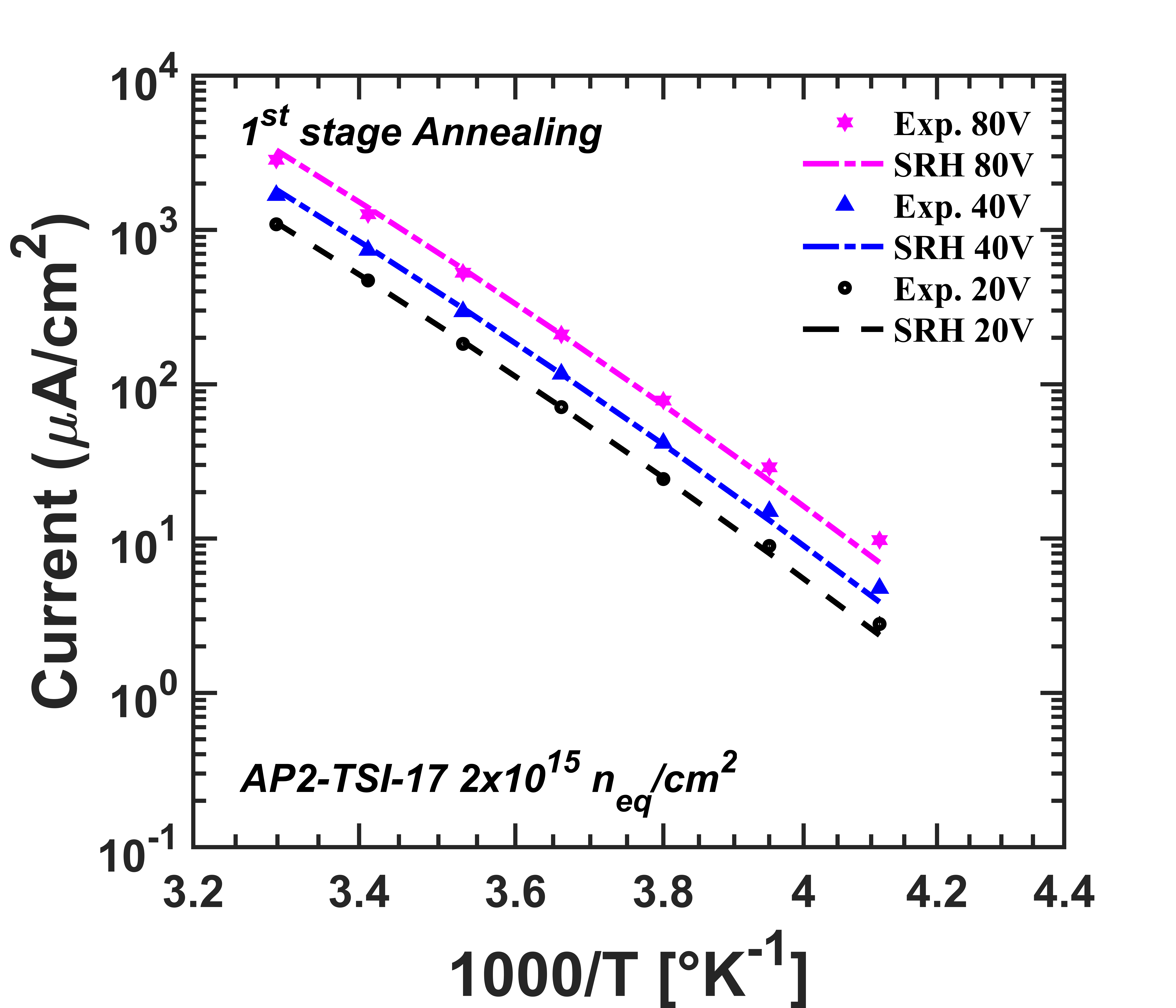
I-V curves of TSI samples (AP2-TSI-06 and AP2-TSI-17, irradiated with and JSI neutrons respectively) after the 1st stage annealing treatment are shown in figure 9a and 9b. The leakage current has been improved by 5 to 10% after the first stage annealing treatment and thus, lower values for are reported (table 5). The breakdown voltage has also been improved by a few volts for these samples. In reference to the section 5.2, the Arrhenius predictions have already been in good agreement with the measurements just after irradiation (before annealing) because the peripheral current becomes negligible in comparison with the increased bulk current. The expected recovery of some radiation-induced defects (both surface and bulk-damage) from the accelerated annealing leads to an improved agreement between the Arrhenius predictions and the measured data, as seen in figure 9c and 9d.
5.3.2 Second stage annealing ( for 30 min)
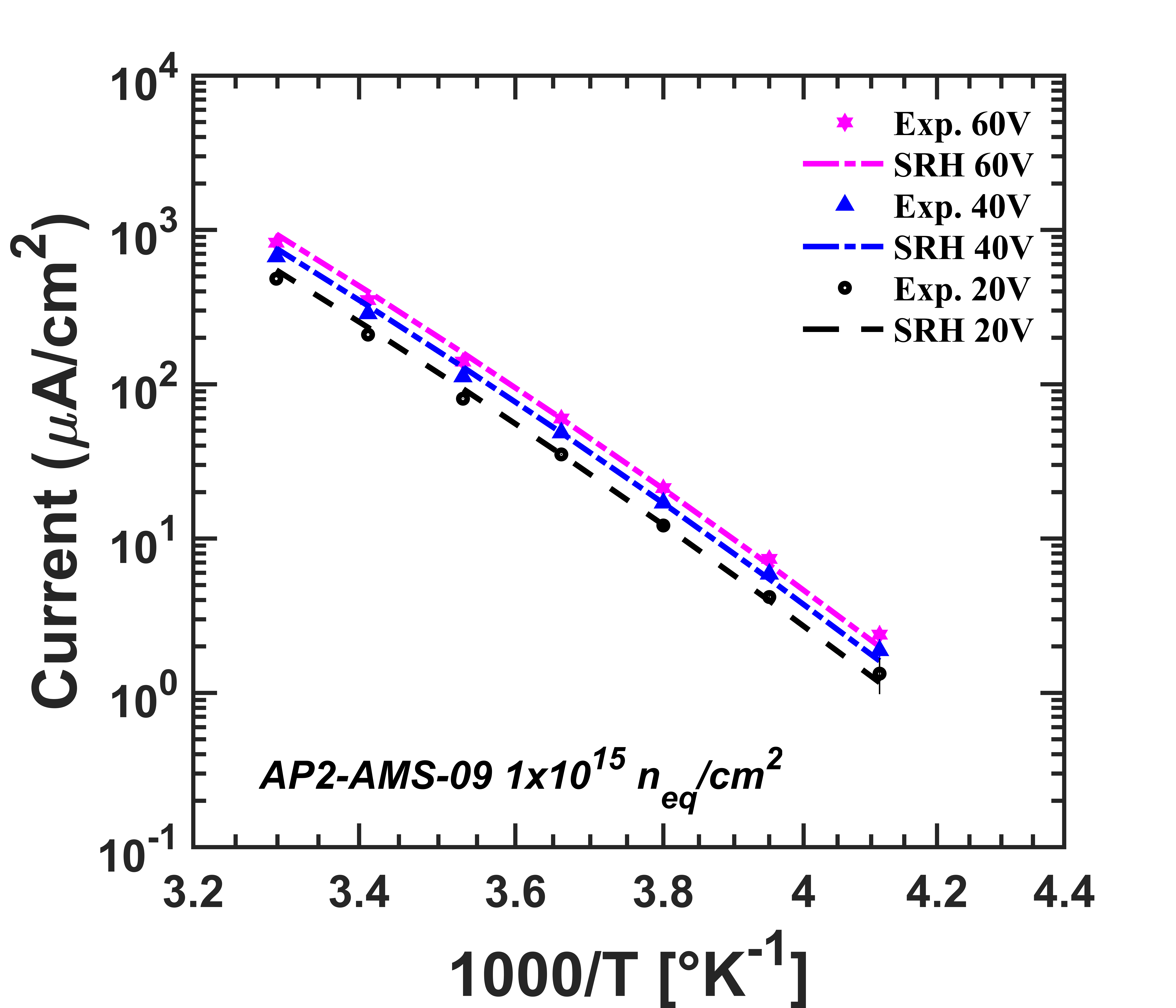
The second stage accelerated annealing was performed on selected candidates from the samples of first stage annealing. Candidates were chosen by cumulative fluence and processing foundry (ams and TSI). Samples were treated for at in the second stage, and a summary of the I-V characteristics can be found in table 6. The leakage current improved by 30% at this stage with respect to the first stage accelerated annealing.
| Fluence | Device ID | Equiv. cum. | |||
| [] | [V] | ann. at | |||
| AP2-AMS-09 | @60 V | @50 V | 71 days | ||
| AP2-TSI-05 | @94 V | @80 V | |||
| AP2-TSI-06 | @92 V | @80 V | |||
| AP2-TSI-17 | @94 V | @80 V |
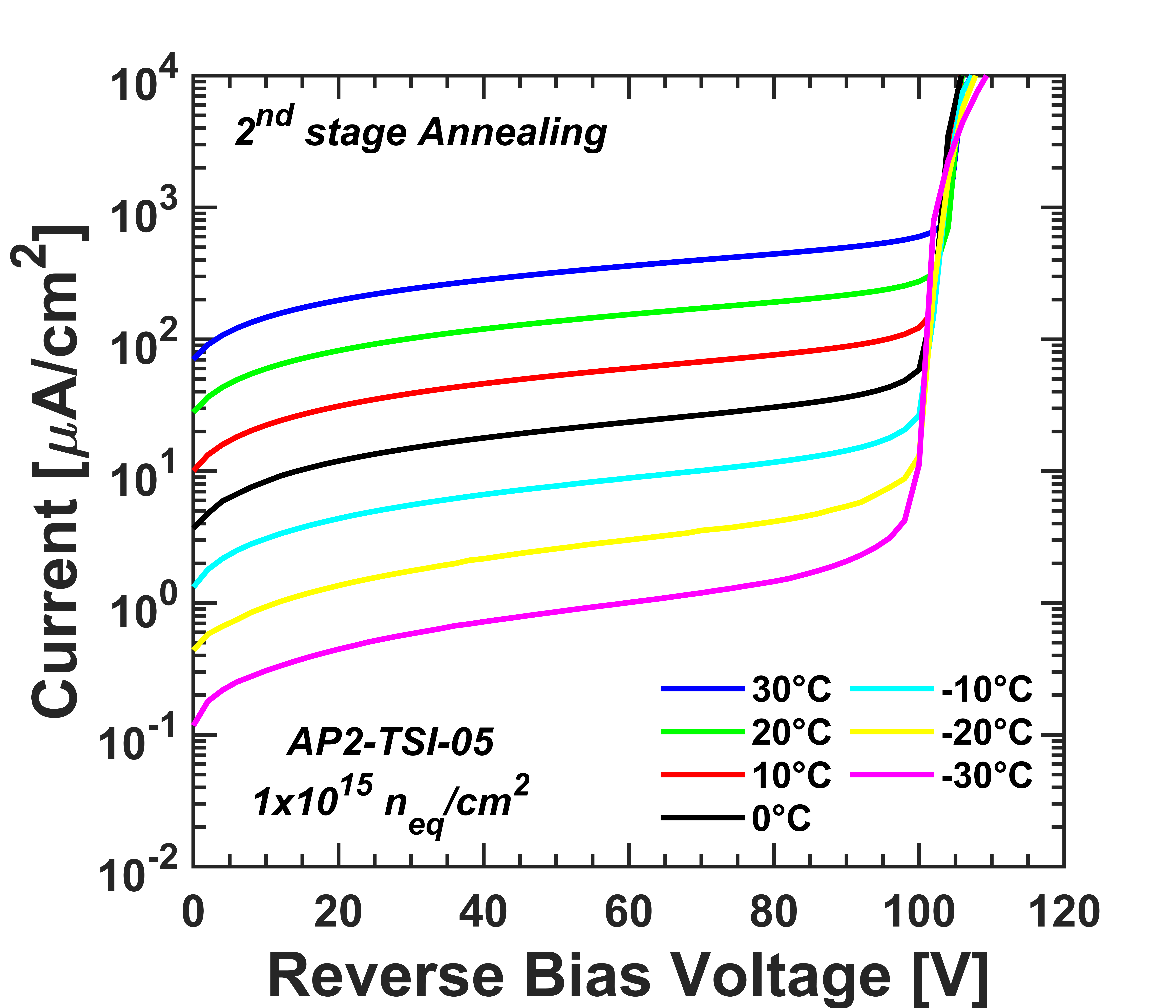
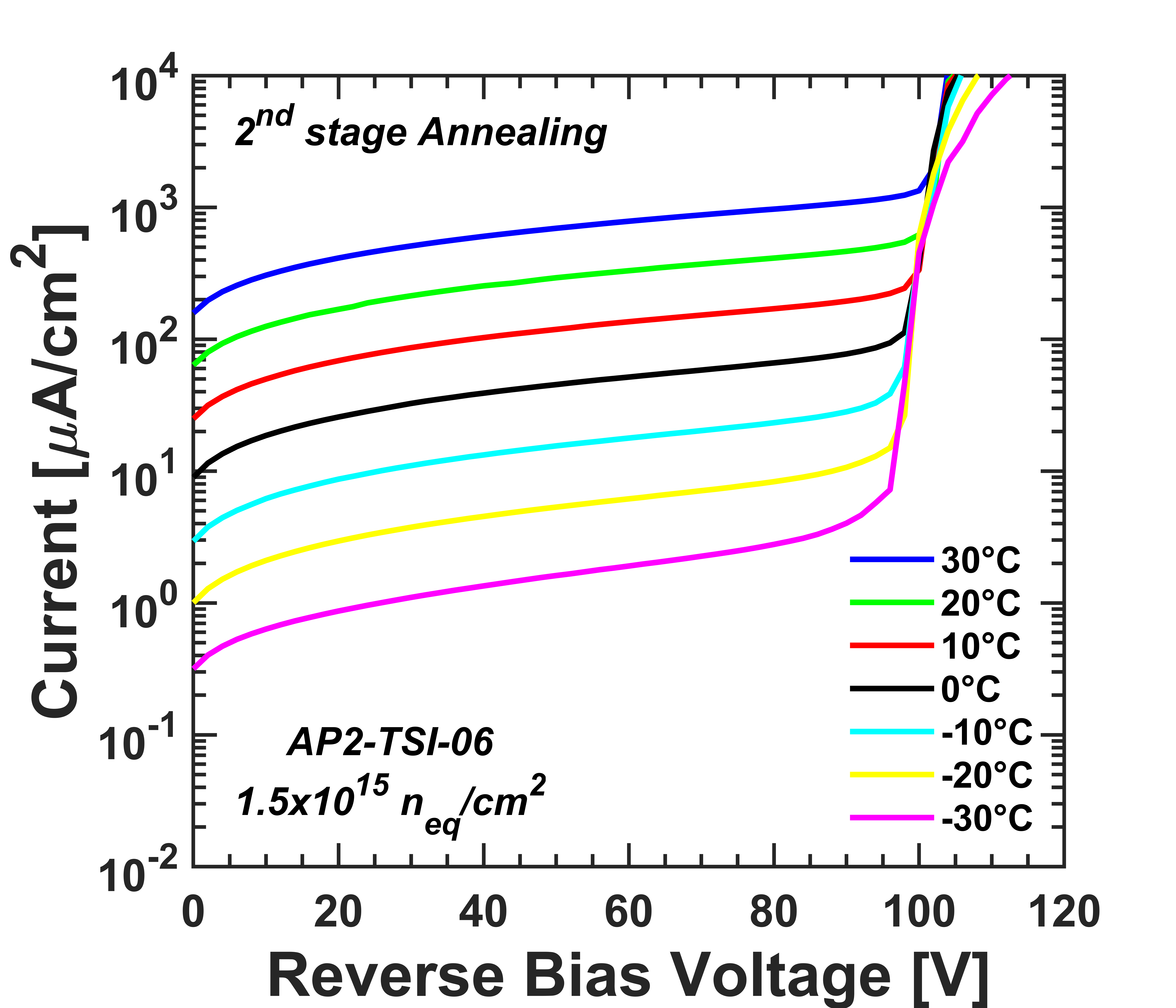
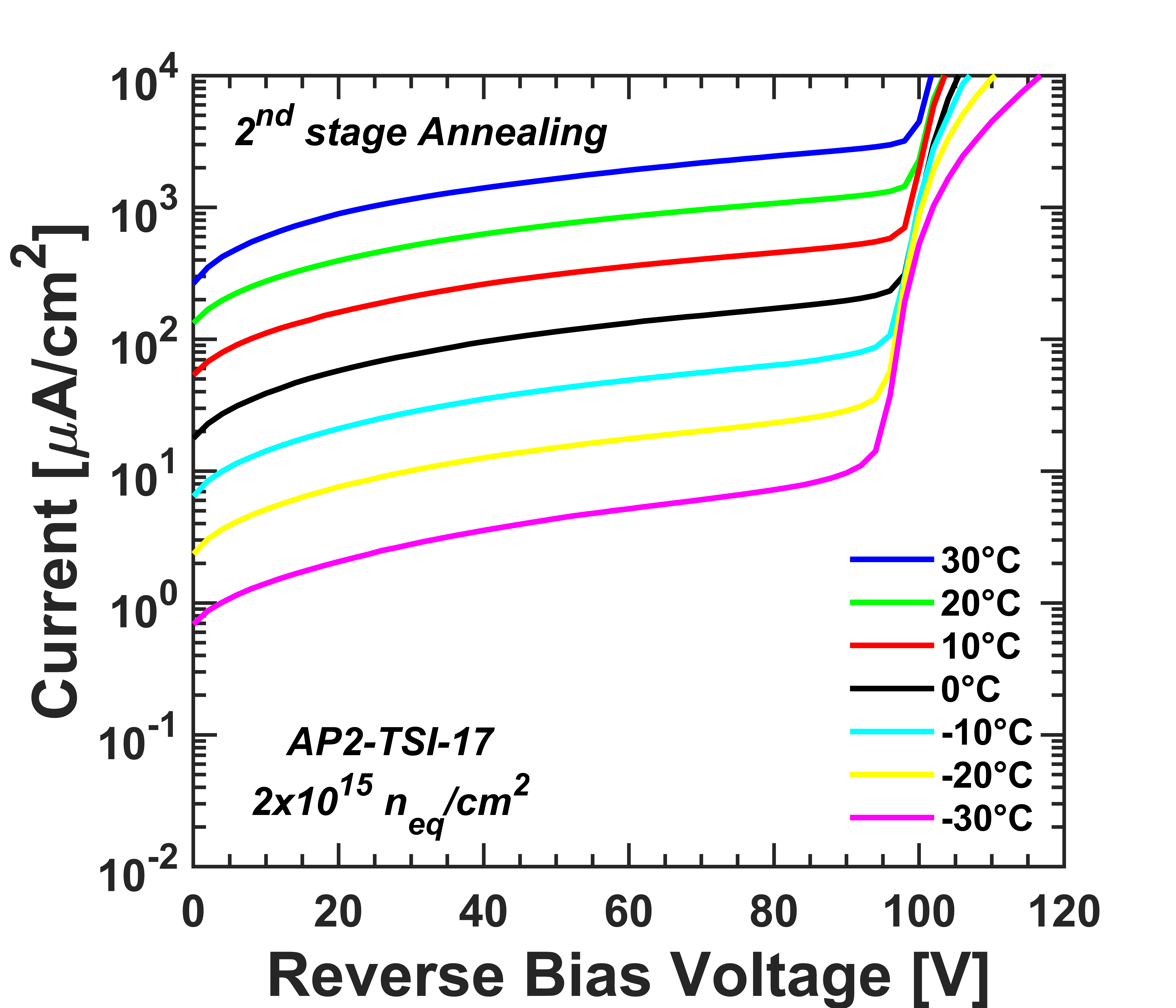
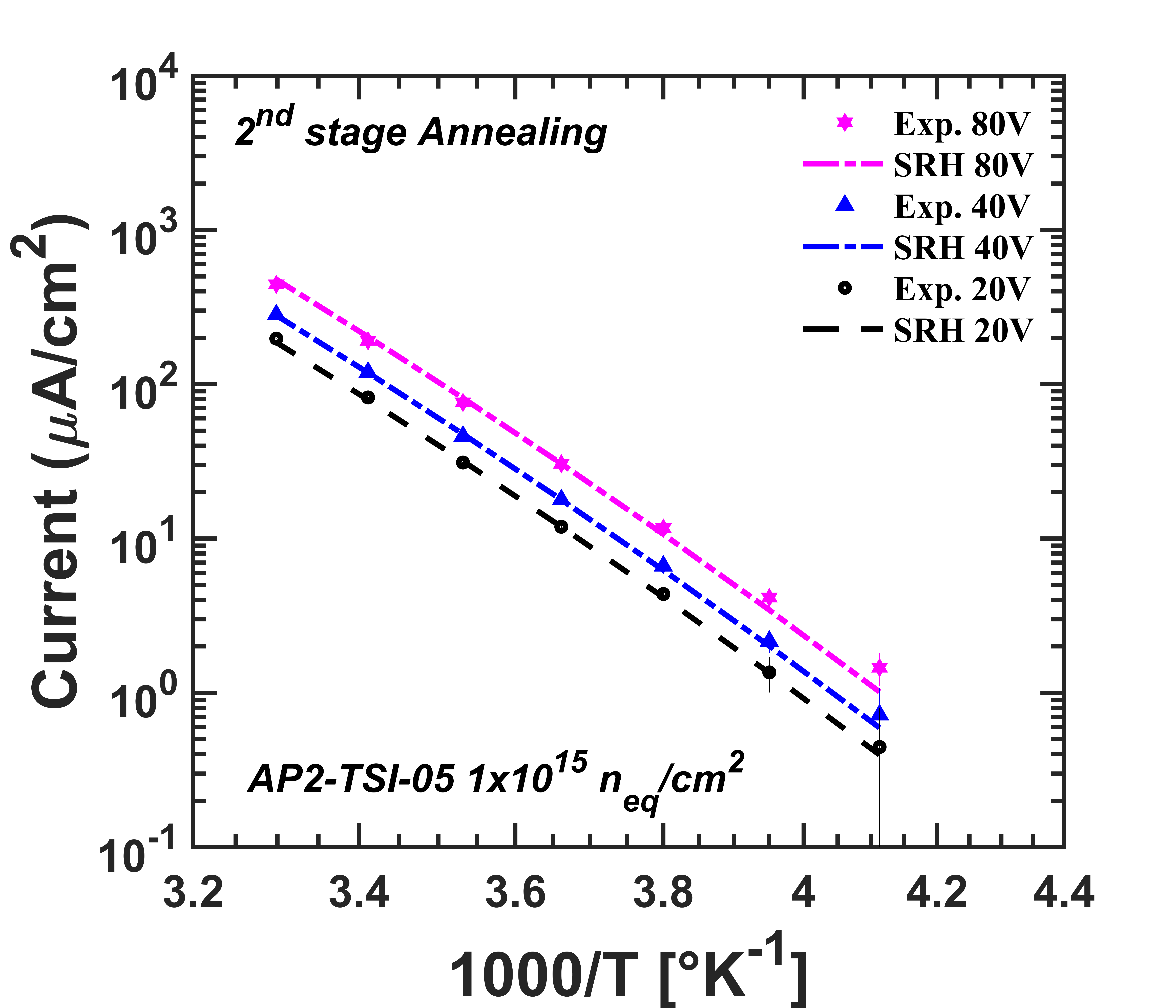
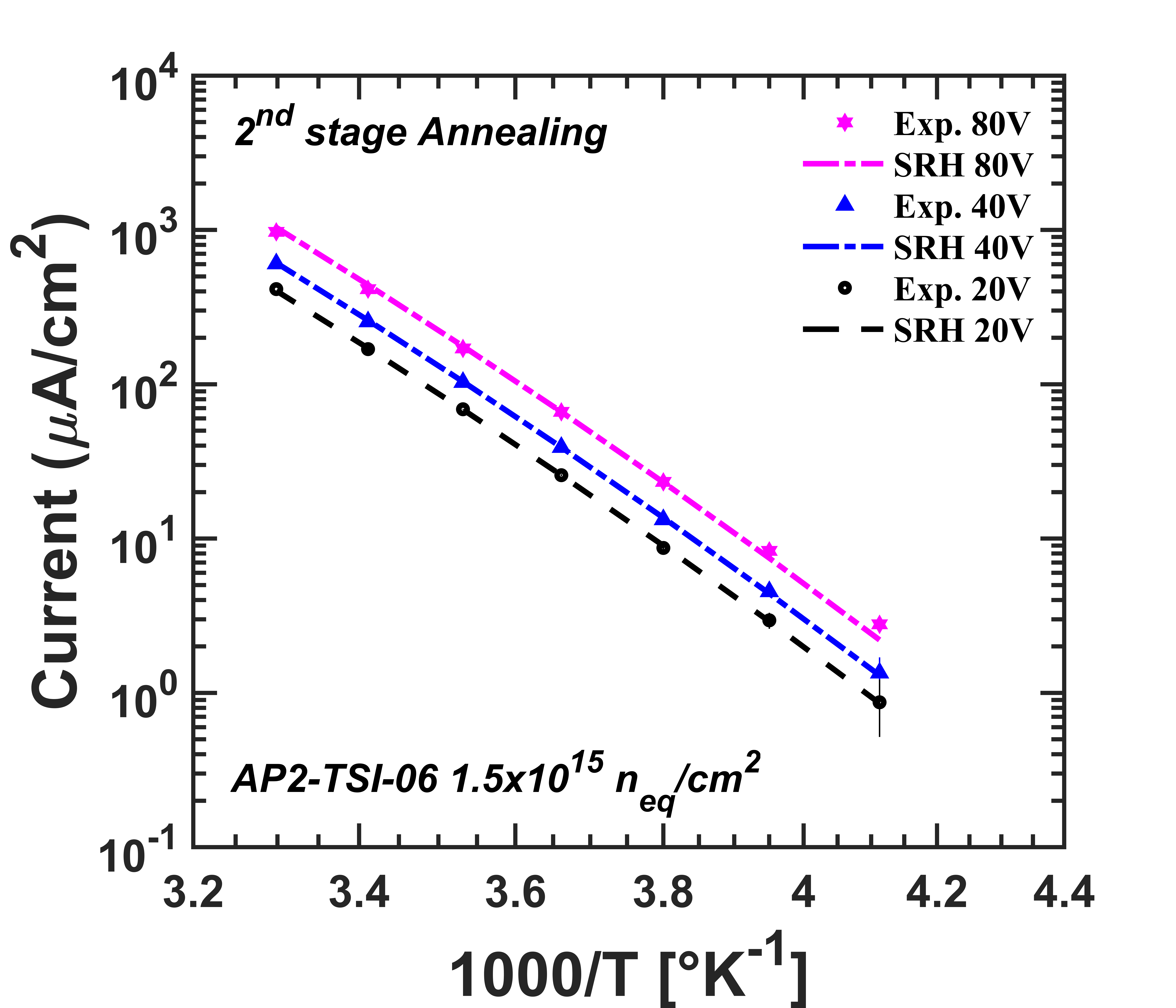

Figure 10 shows the I-V characteristics measured on TSI samples (irradiated with different fluences of neutron) after the second stage of accelerated annealing. The breakdown voltage tends to improve by a few volts due to the same reason of recovering the interface states and traps by annealing treatments. The surface conditions for TSI samples helped to trigger a delayed impact ionization. The corresponding Arrhenius plots also shows a good agreement for the measured data with the thermionic generation model.
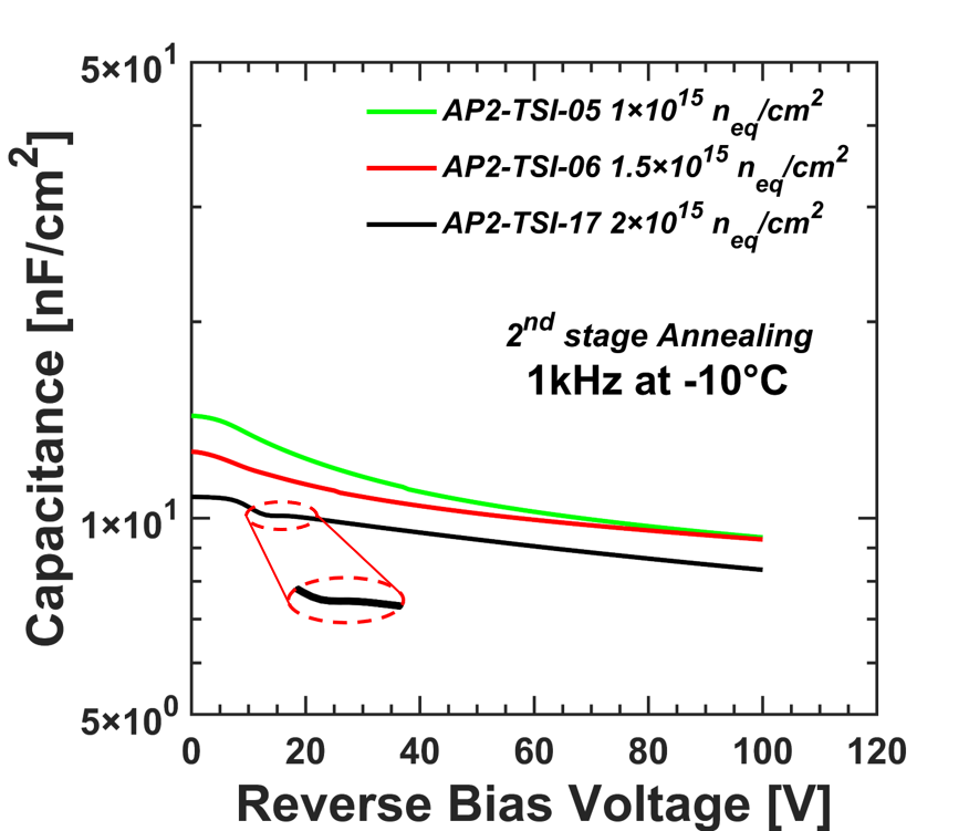
C-V data shown in figure 11 measured after the second stage annealing for an AC signal of and a frequency. They are quite comparable to the data seen before annealing, meaning there is no additional effect from these annealing treatments up to this second stage.
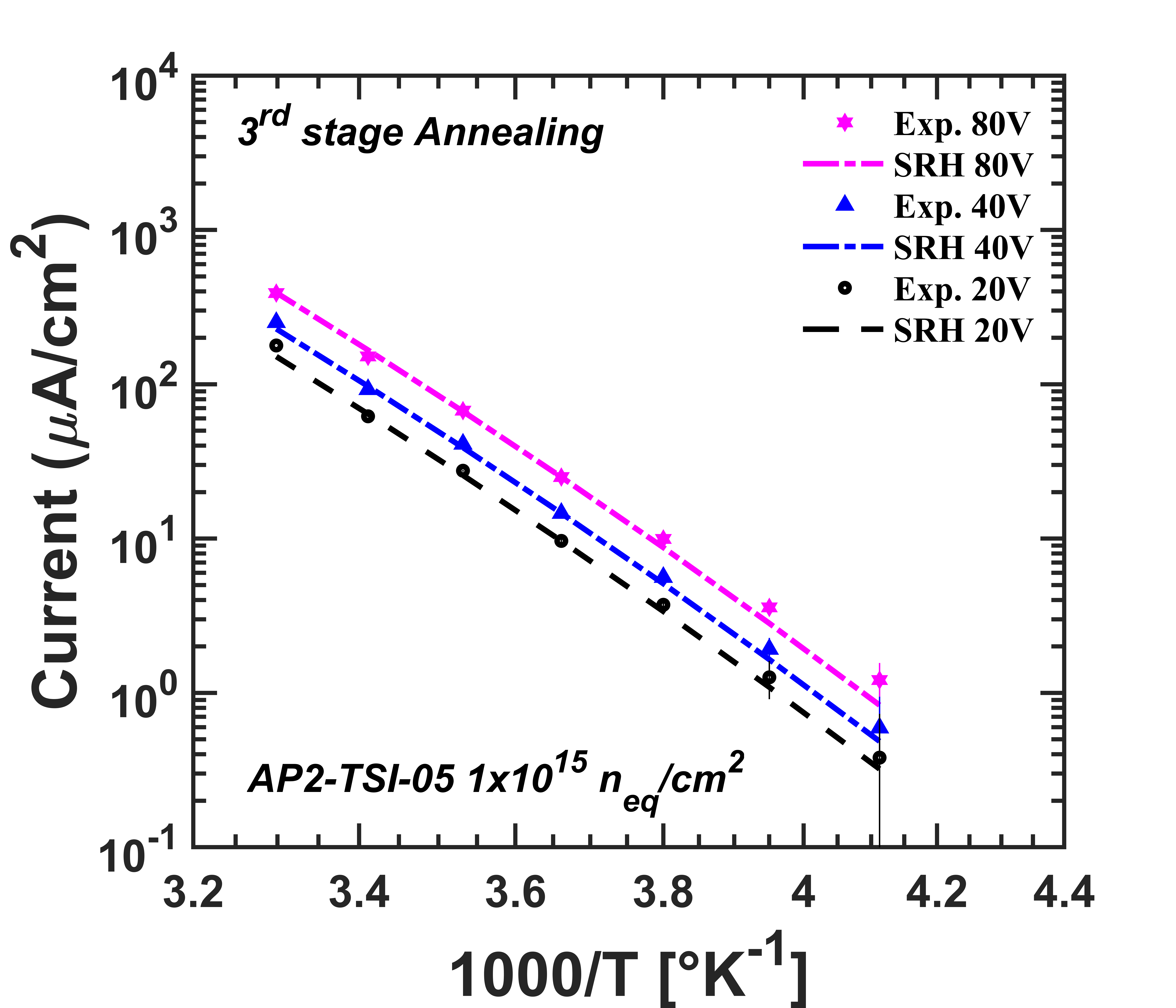
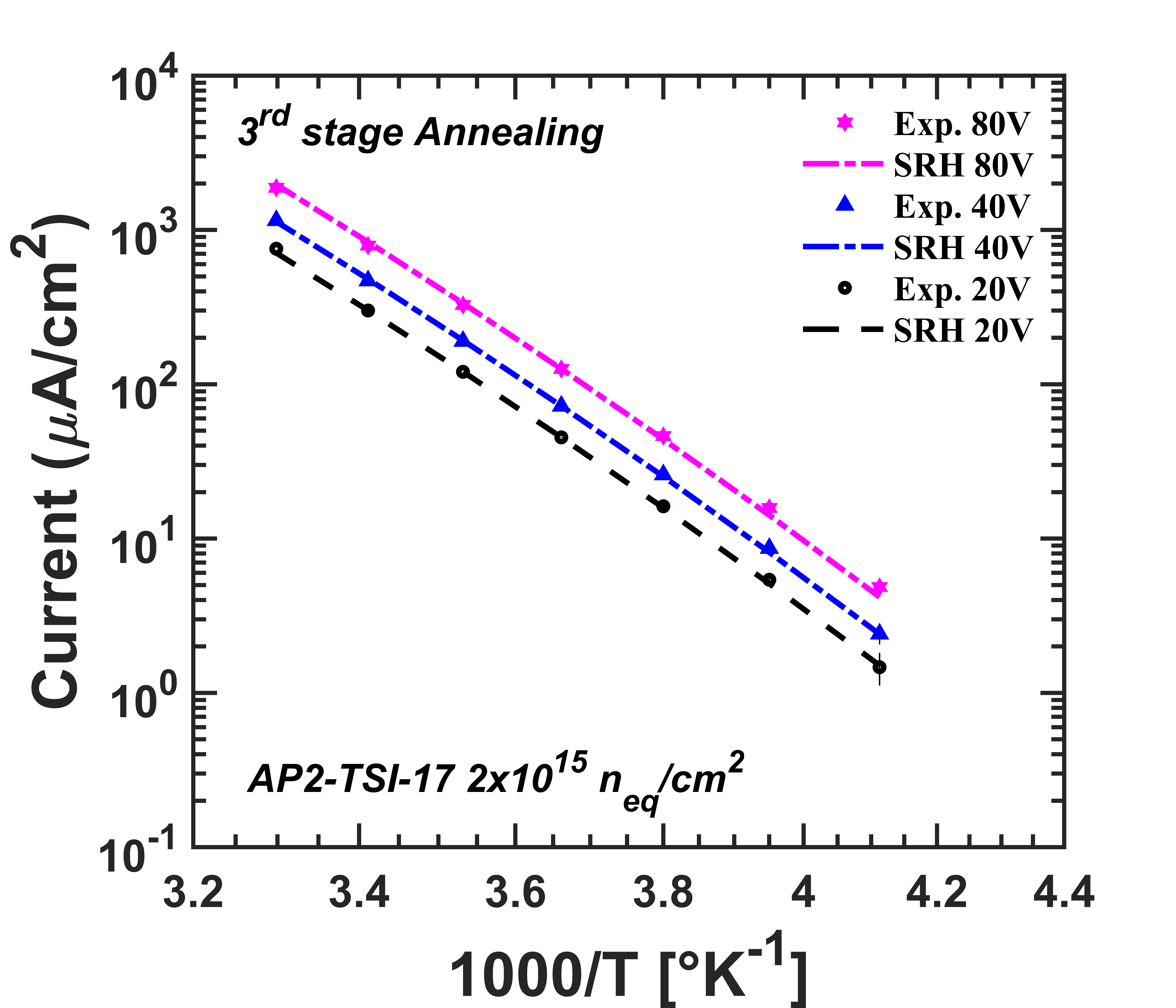
5.3.3 Third stage annealing ( for 120 min)
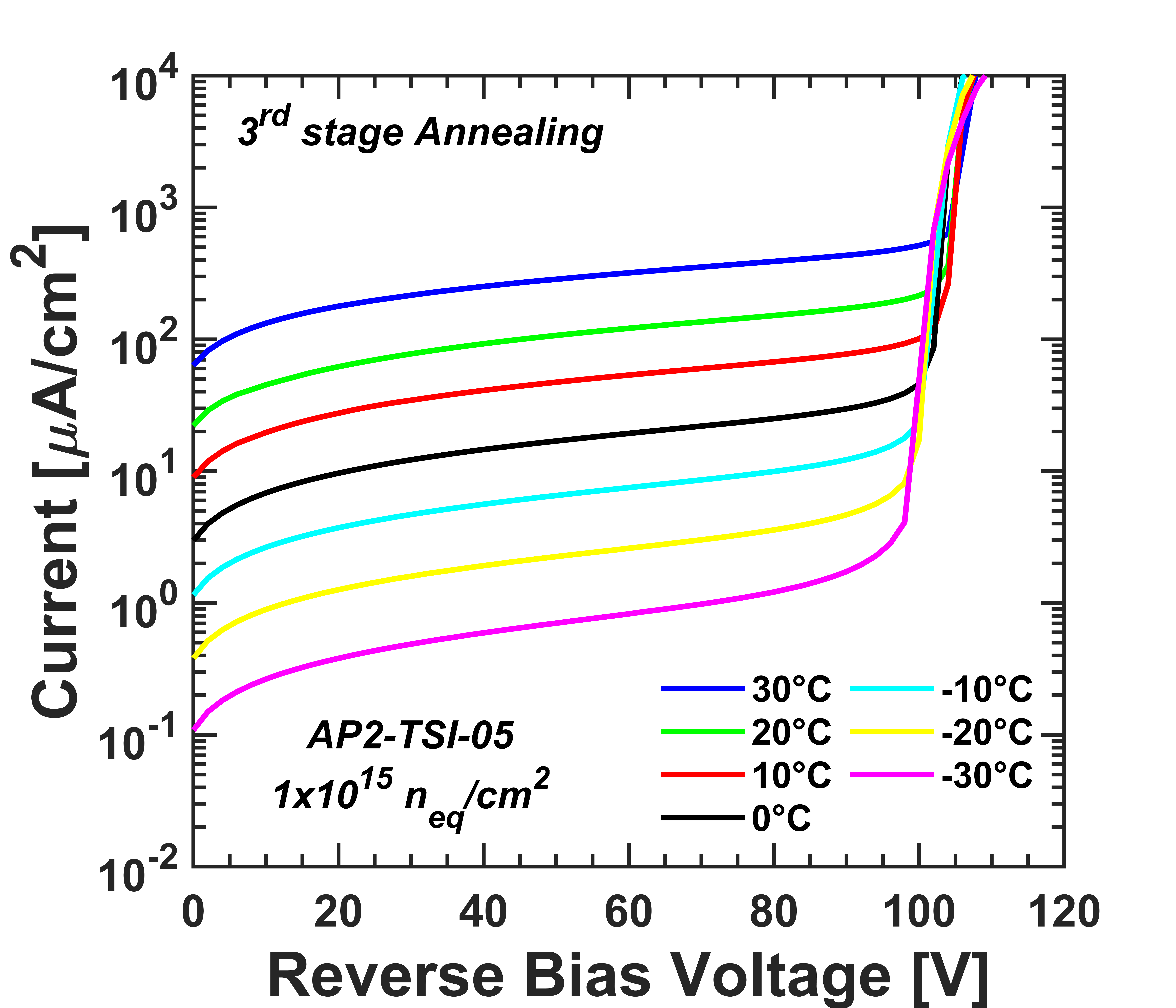
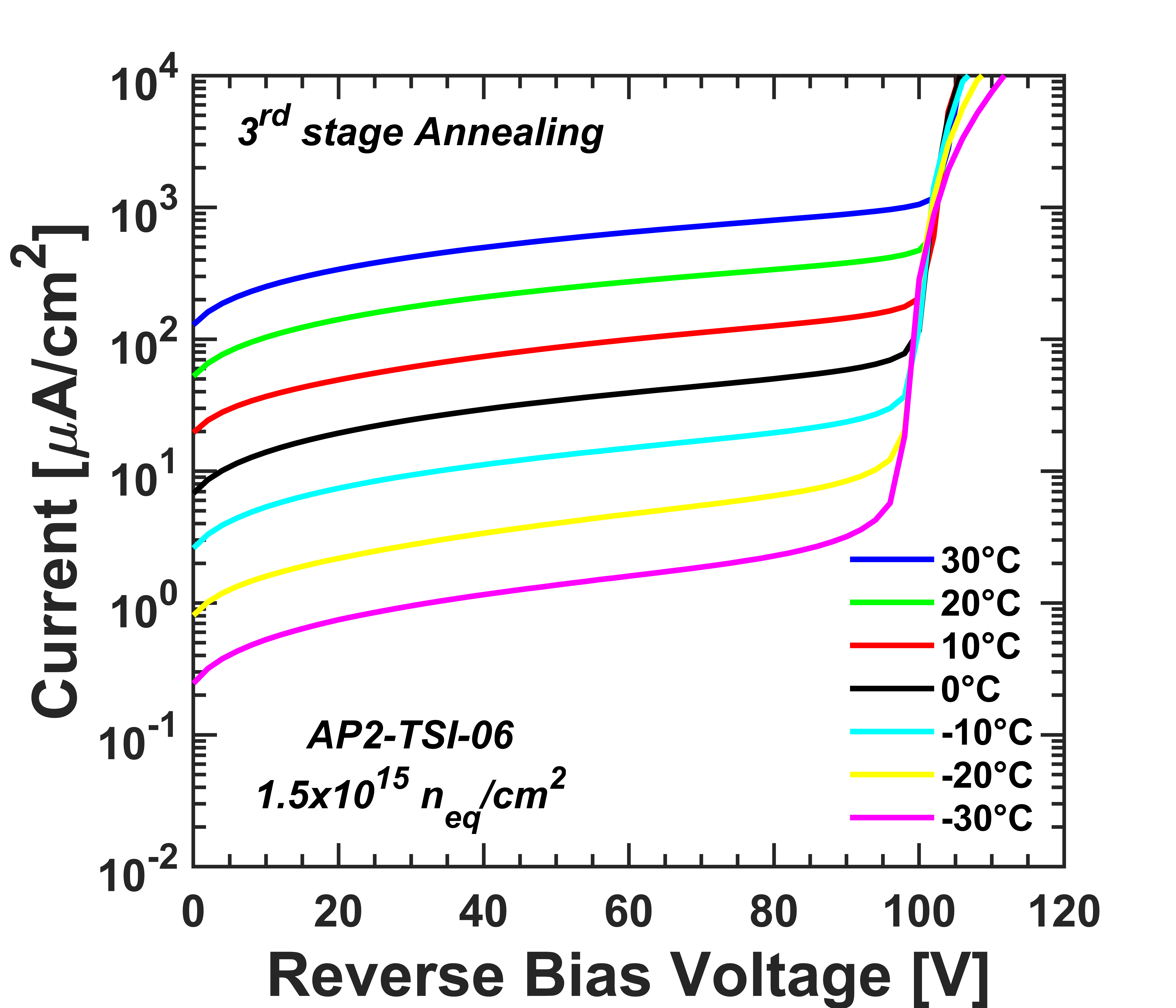
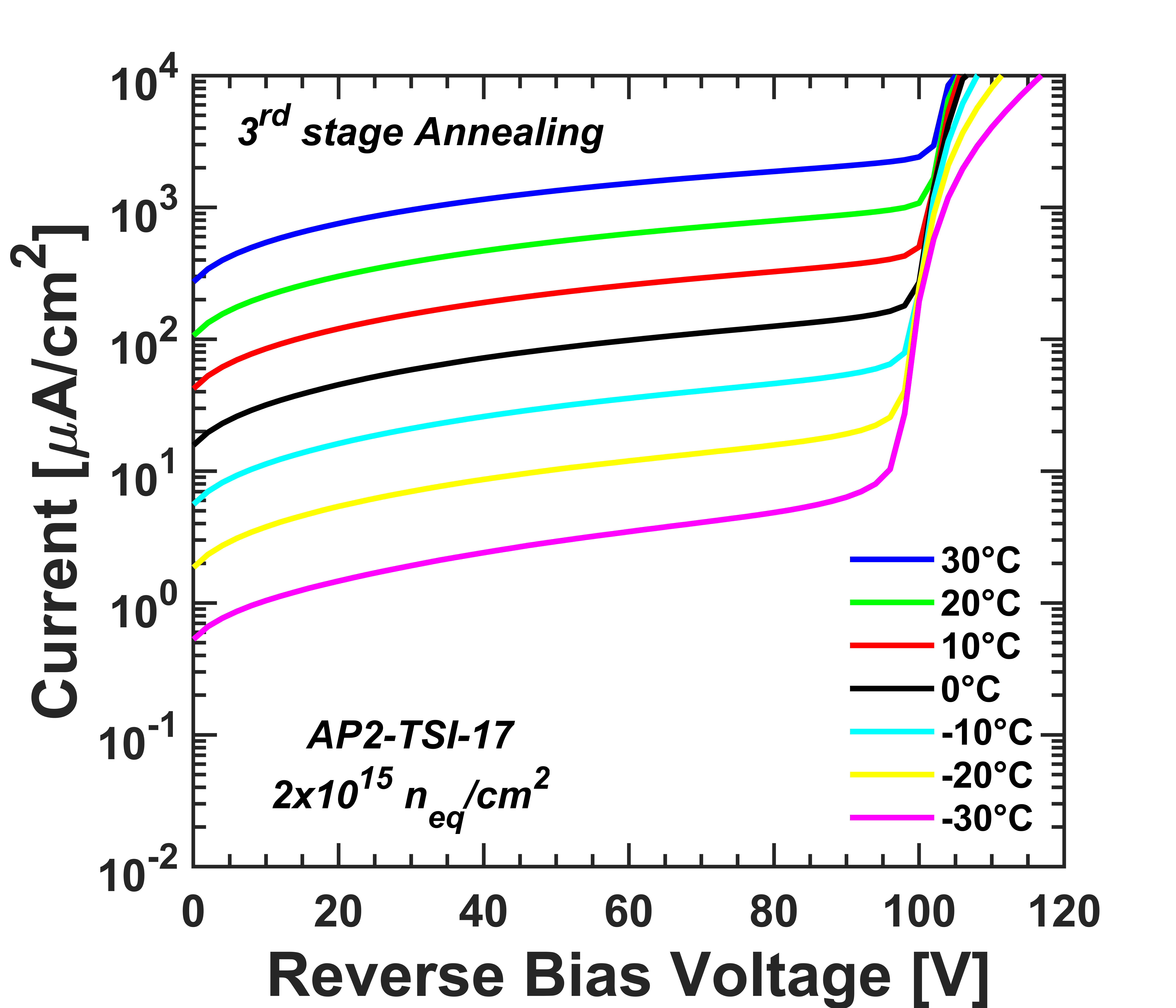
Same selected samples used for second stage of accelerated annealing were further annealed for at in the third stage. The summary of I-V characterizations is reported in table 7. The breakdown voltage increased by few volts for sample AP2-TSI-17 after the third stage annealing, as expected. Figure 12 shows the measured I-V data of the TSI samples after the third stage annealing, where Arrhenius predictions are still in good agreement (irrespective of the fluence) with the measured data.
| Fluence | Device ID | Equiv. cum. | |||
| [] | [V] | ann. at | |||
| AP2-AMS-09 | @60 V | @50 V | 359 days | ||
| AP2-TSI-05 | @94 V | @80 V | |||
| AP2-TSI-06 | @94 V | @80 V | |||
| AP2-TSI-17 | @96 V | @80 V |

5.3.4 Fourth stage accelerated annealing ( for 300 min)
Samples treated with third stage annealing were again treated for a long accelerated annealing at in the fourth stage. There was no sign of full depletion for the C-V data of TSI prototypes, reported in figure 13. However, the lateral depletion has still been seen at for the sample AP2-TSI-17 (irradiated with neutrons).
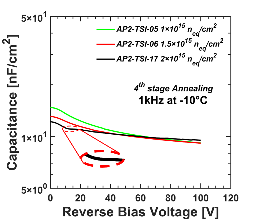
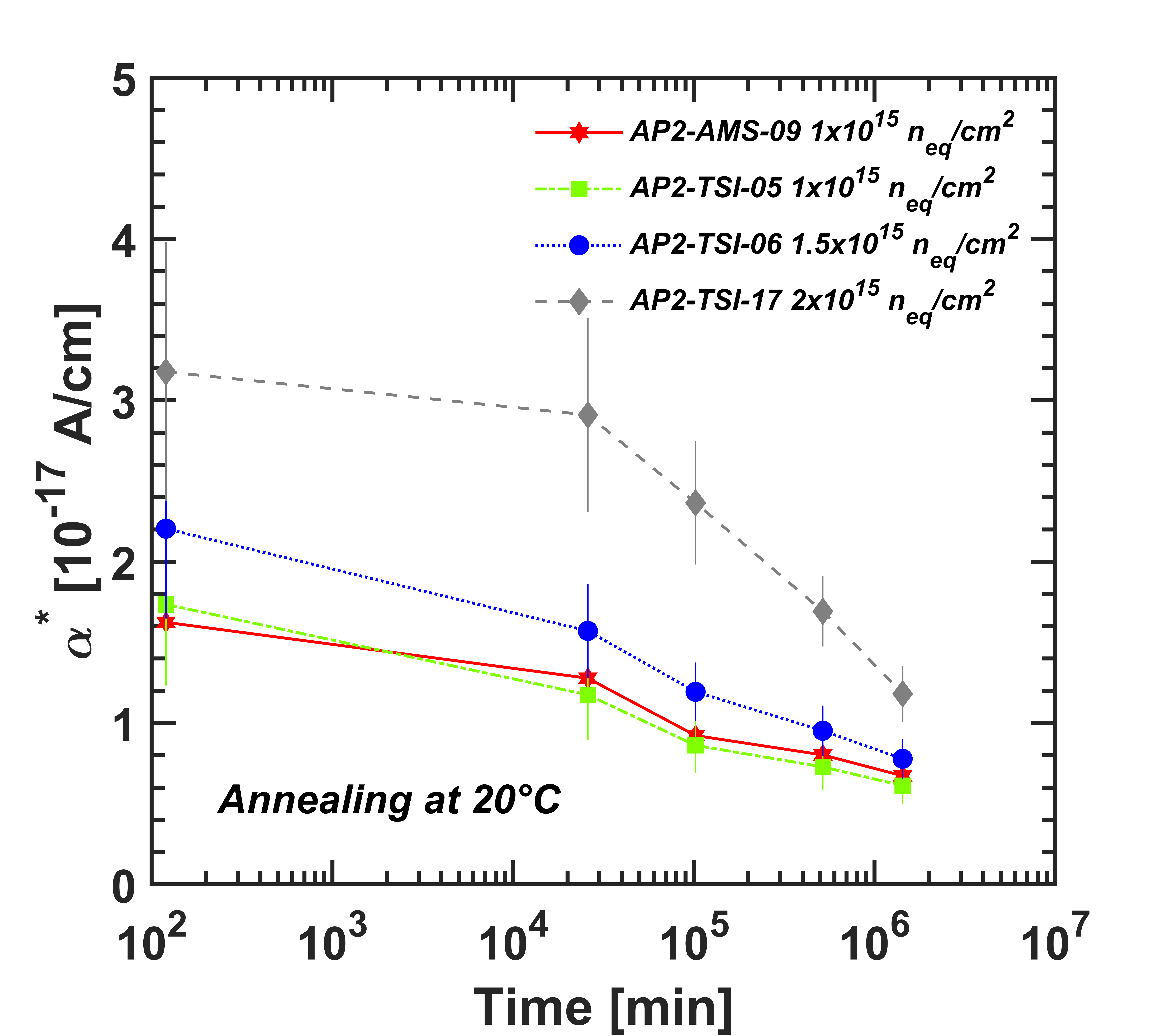
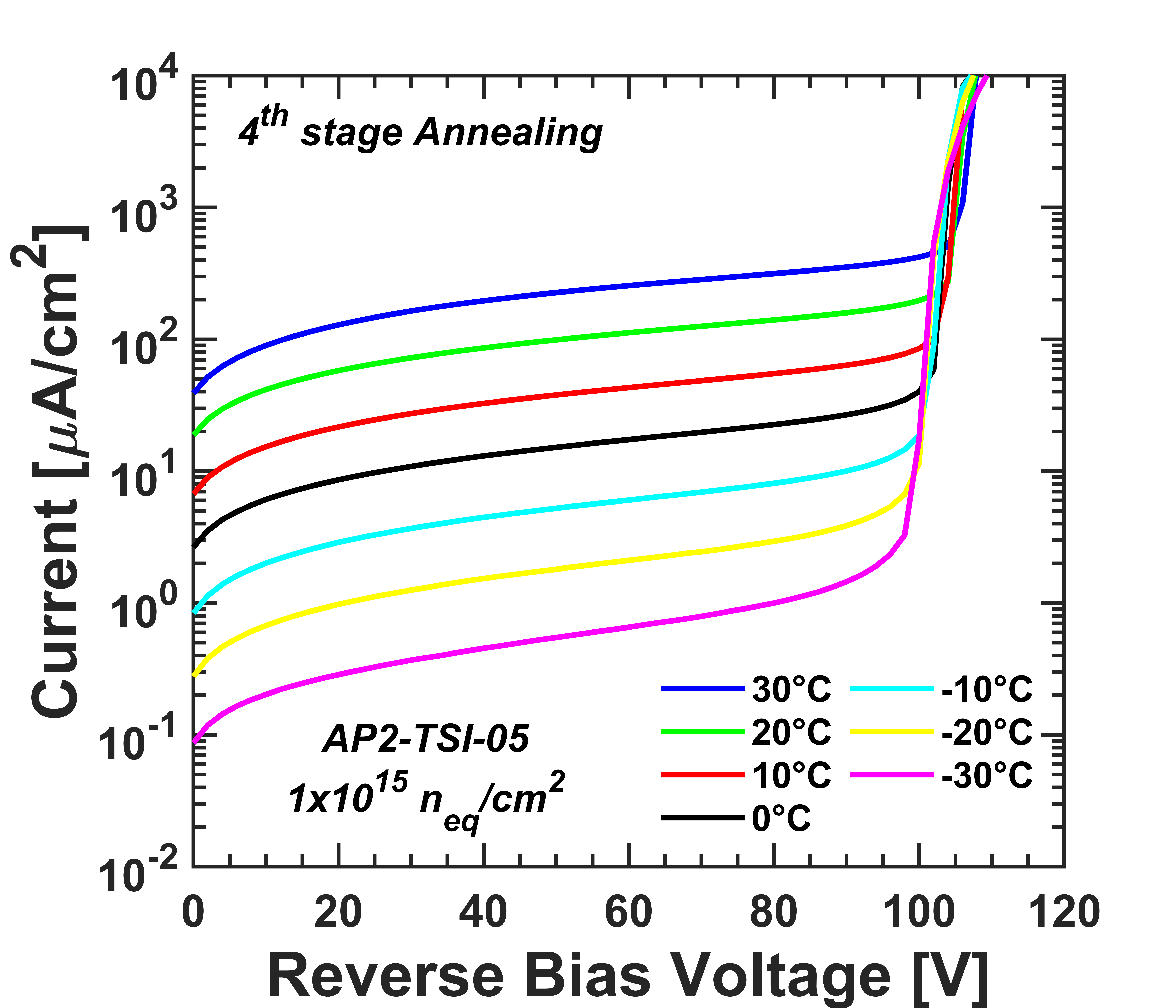
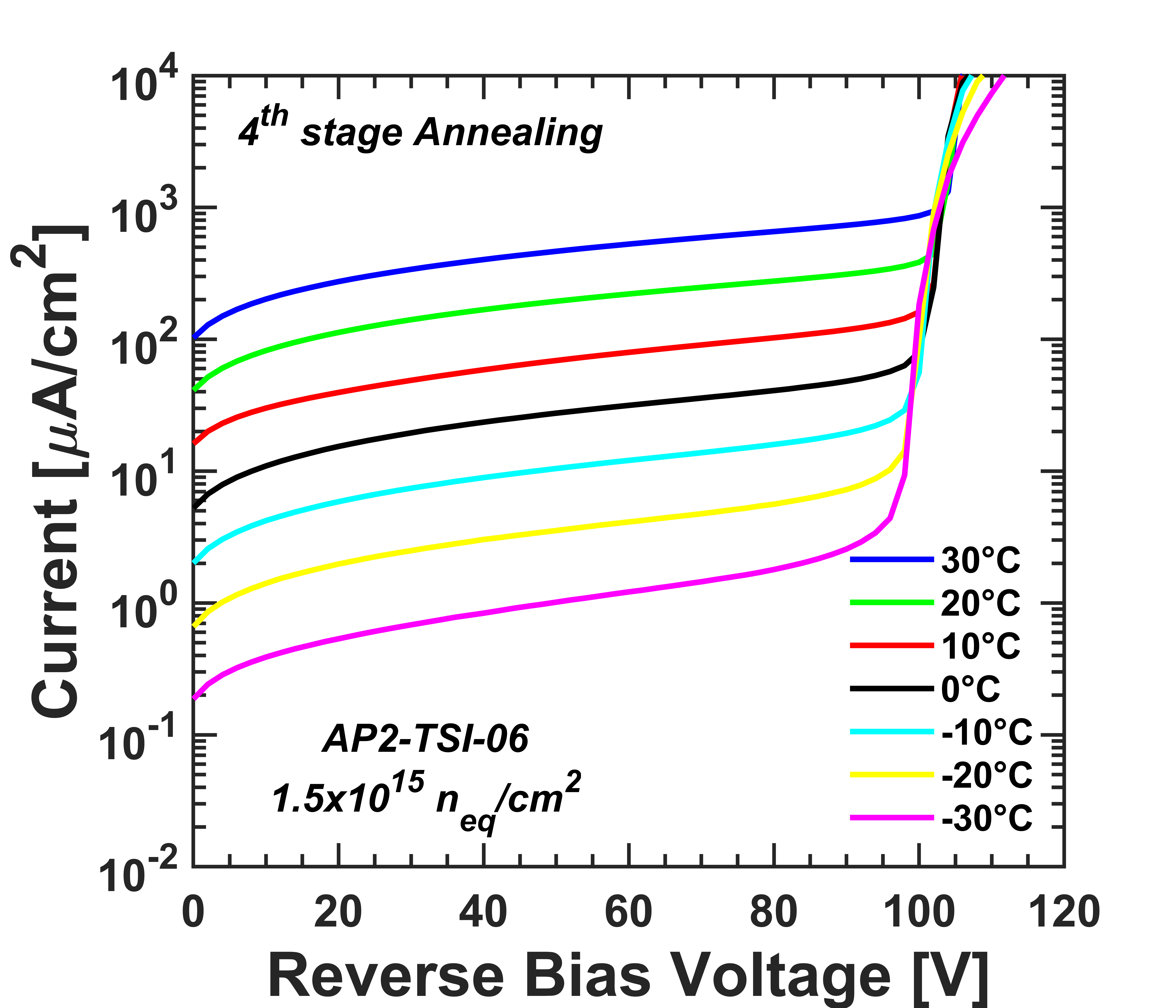
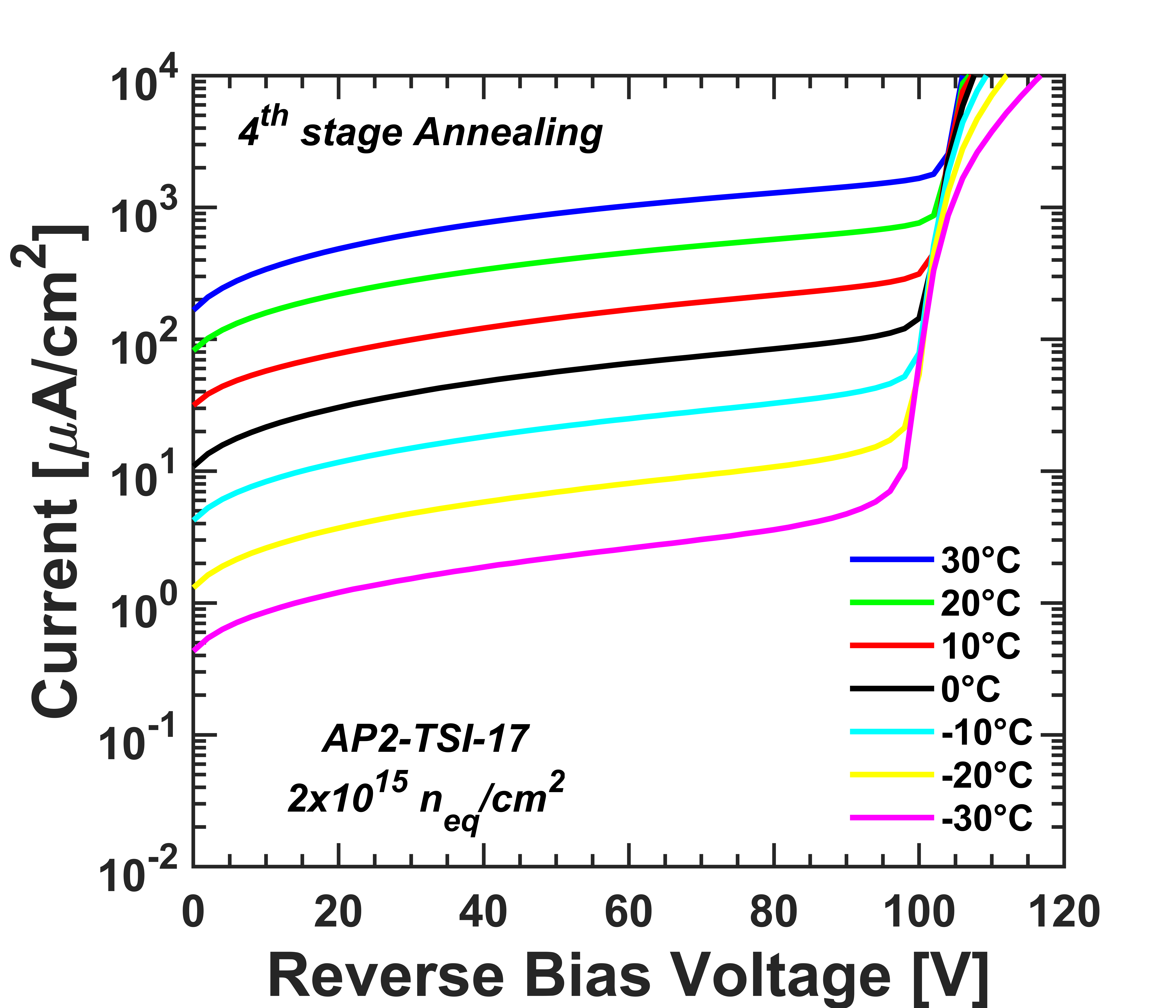
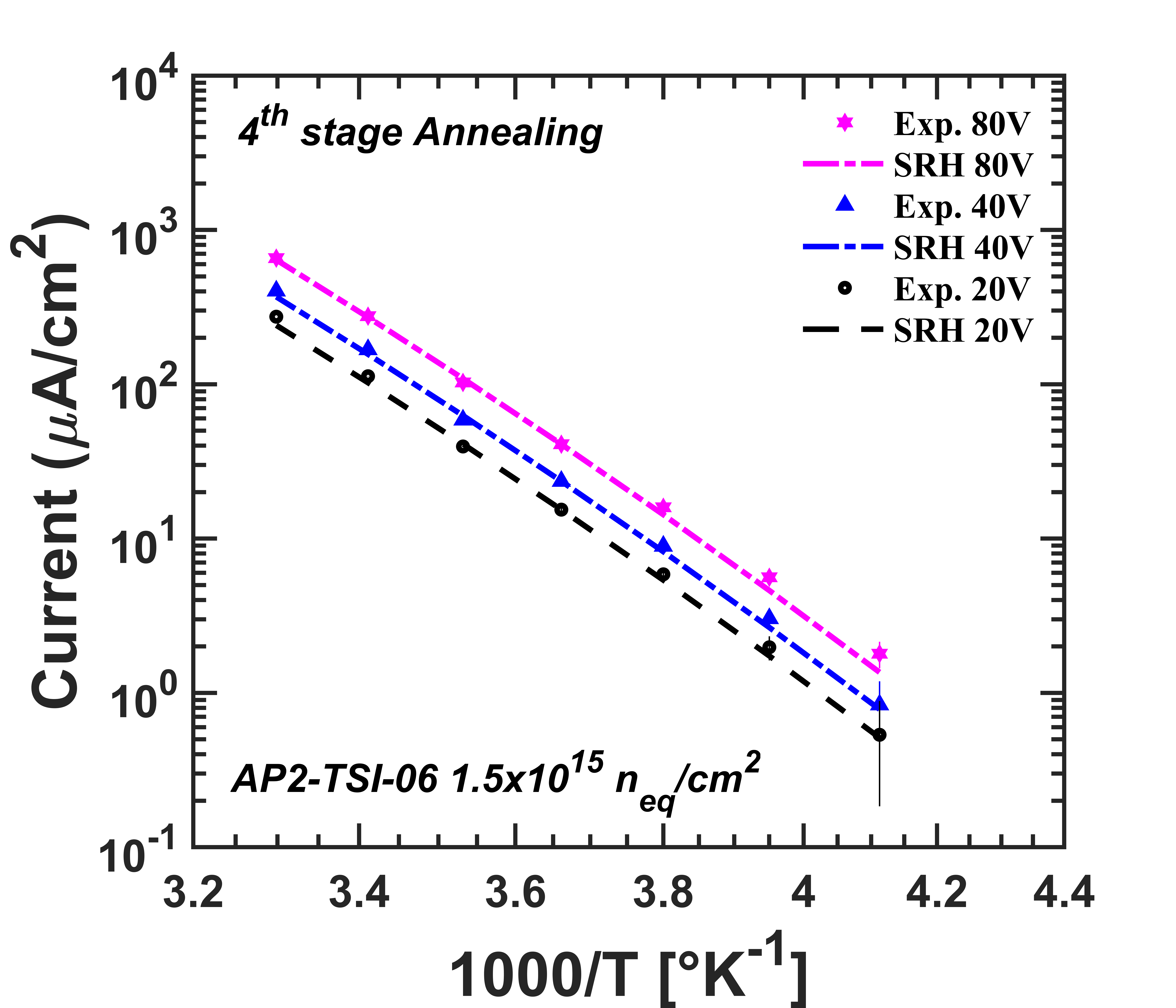
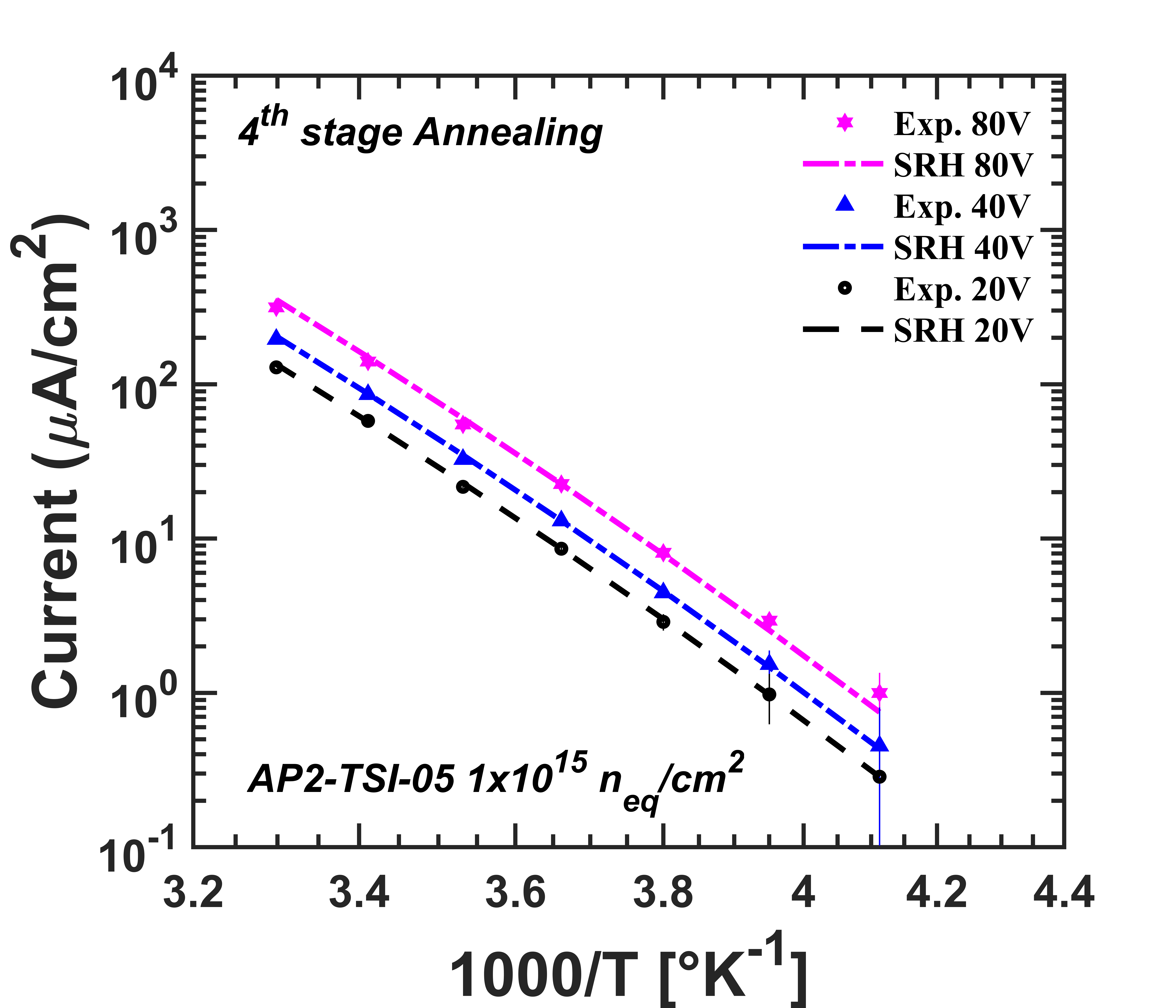

Table 8 summarizes all electrical characteristics of the selected samples after the fourth stage annealing. I-V measured at different ambient conditions and the corresponding Arrhenius plots can be found in figure 14. TSI sample’s breakdown after the fourth stage annealing is almost (irrespective of the irradiation fluence), as it was seen for TSI non-irradiated prototypes, meaning beneficial annealing played the major role in all annealing stages. A few volts lower breakdown voltage has been observed for the ams sample (table 8) in comparison to the first stage accelerated annealed data (table 5). This can be explained from the peripheral current of ams sample. The interface states and traps are recovered by accelerated annealing and the peripheral current contributes to trigger an early impact ionization.
| Fluence | Device ID | Equiv. cum. | |||
| [] | [V] | ann. at | |||
| AP2-AMS-09 | @58 V | @50 V | 993 days | ||
| AP2-TSI-05 | @94 V | @80 V | |||
| AP2-TSI-06 | @94 V | @80 V | |||
| AP2-TSI-17 | @96 V | @80 V |
Figure 13b summarizes the improvement of leakage current related damage rate, in correspondence to the equivalent near room temperature annealing () (numerically calculated). The very first values for samples of different fluences are representative to the leakage current after irradiattion but before applied annealing steps.
It is worth noting that has been decreased by a factor of 2 for prototypes (exposed to all fluences). The values are, within uncertainties, in very good agreement with the exponential-logarithmic model of leakage current [15]. The ams chip shows a larger damage constant at for neutrons irradiation (figure 13b). In fact, the data for TSI chip has been reported for a higher reverse bias, . Peripheral current in the ams chip would have contributed to this visible discrepancy.
6 Conclusions
Electrical characterizations have been extensively performed on ATLASPix2 prototypes produced by both ams AG and TSI Semiconductors on MCz 20 P-type substrate. TSI produced ATLASPix2 prototypes appeared better than ams samples in terms of leakage current and breakdown voltage. Non-irradiated TSI samples reported breakdown voltage at greater than , very well in agreement with HV-CMOS technology design standards. In contrast, ams ATLASPix2 samples reported a breakdown voltage of before irradiation, as seen in their predecessor, the ATLASPix1. The leakage current of TSI samples before irradiation were found to be a fraction of at , which is a factor of 5 to 6 less than for the ams prototypes. SRH prediction before irradiation shows a good agreement with the measured data (up to ) for TSI prototypes and the disagreement seen at the lower temperatures has been driven by carrier ionization rate increase.
To understand the radiation hardness property of the ATLASPix2 sensor-diodes, samples from both foundries were irradiated up to neutrons. After irradiation, measured I-V data for the samples of both foundries were found in good agreement with the SRH model (irrespective of the cumulated fluences), meaning the effect of surface current and ionization rate increase at lower temperature become less significant. The leakage current of TSI samples is a factor of two less than for ams AG prototypes at any respective reverse bias (earlier than avalanche breakdown). For prototypes from both foundries irradiated at a higher fluence, the leakage current increases, as expected. It is also worth noting that the radiation hardness property of pixel-electronics has been beyond the scope of this paper, that would require additional functional-tests.
Irradiation induces surface interface states and bulk-traps, which help to seize peripheral carriers and delay the impact ionization process, as observed in ams AG samples. Thus, the breakdown voltage has been improved by around after irradiation. In the case of irradiated TSI prototypes, an early breakdown voltage driven by impact ionization effect (10 to less) is observed in comparison to non-irradiated samples. C-V data measured at irradiated samples shows a few hundreds of , are comparable to an initial two-dimensional TCAD simulation result. The lateral depletion plateau has also been seen for samples of higher irradiation fluences ( and neutrons) at , determining the minimal reverse bias required for the sensor operation to obtain a full depletion laterally around the pixel diodes.
In an aim to study the annealing impact on ATLASPix2 prototypes, a systematic annealing study has been performed on prototypes of both foundries. Four stages of accelerated annealing applied for ATLASPix2 prototypes, where the cumulative equivalent time can be estimated to 33.1 months-long room temperature annealing (). Beneficial annealing seems to play the major role as leakage related damage-rate () decreased even after the fourth stage of accelerated annealing. The breakdown voltage for all samples shows a trend to reach its non-irradiated condition, as expected from annealing driven damage recovery. The lateral depletion observed in C-V data (after annealing treatments) has been seemed unaffected. A dedicated C-V measurement of a thinner sensor (comparable to the actual depletion depth) may give a better picture of what can happen at full depletion, and it is yet to be investigated.
Regardless of uncertainties, primarily those in the irradiation fluences, depleted volumes and annealing conditions, which would have an impact on the measured values, the leakage current behavior of TSI samples did not show anomalous deviations from the theoretical expectations. The breakdown voltage remained greater than for the highest fluence of neutrons considered within this study. The electrical properties variation through annealing are dominated by the beneficial kind, for a length of time corresponding to a scenario where sensors may remain at room temperature for more than two years in a foreseen long shutdown.
Acknowledgments
Authors acknowledge Prof. Vladimir Cindro and Dr. Igor Mandic from JSI, Ljubljana for their support in the neutron irradiation. This project received funding from the SNSF grants 200021_169015, 200020_156083, 20FL20_173601 and 200020_169000.
References
- [1] ATLAS Collaboration, Technical Design Report for the ATLAS Inner Tracker Strip Detector, CERN-LHCC-2017-005 (2017).
- [2] ATLAS Collaboration, Technical Design Report for the ATLAS Inner Tracker Pixel Detector, CERN-LHCC-2017-021 (2018).
- [3] ams AG, Austria, https://ams.com/process-technology#highvoltagecmos.
- [4] TSI Semiconductors, USA, http://www.tsisemi.com/process.
- [5] I. Peric et al., A high-voltage pixel sensor for the ATLAS upgrade, Nuclear Inst. and Methods in Physics Research, A 924 (2019) 99-103.
- [6] D M S Sultan et al., Electrical characterization of AMS aH18 HV-CMOS after neutrons and protons irradiation, 2019 JINST 14 C05003.
- [7] TOPSIL, Denmark, http://www.topsil.com/en/silicon-products/silicon-wafer-products.aspx.
- [8] K. Ambrozic et al., Computational analysis of the dose rates at JSI TRIGA reactor irradiation facilities, Applied Radiation and Isotopes, 130 (2017) 140, ISSN: 1872-9800.
- [9] I. Mandic et al., Bulk Damage in DMILL npn Bipolar Transistors Caused by Thermal Neutrons Versus Protons and Fast Neutrons, IEEE Transactions on Nuclear Science, 53 (2004) 4.
- [10] FormFactor, 7005 Southfront Road, Livermore, CA 94551 (USA). https://www.formfactor.com/.
- [11] N. Bacchetta et al., Improvement in breakdown characteristics with multiguard structures in microstrip silicon detectors for CMS, Nucl. Instrum. Meth. A 461 (2001) 204.
- [12] G.-F. Della Betta et al., Investigation of leakage current and breakdown voltage in irradiated double-sided 3D silicon sensors, 2016 JINST 11 P09006.
- [13] A. Chilingarov, Temperature dependence of the current generated in Si bulk, 2013 JINST 8 P10003.
- [14] C. R. Crowell et al., Temperature Dependence of Avalanche Multiplication in Semiconductors, Applied Physics Letter 9 (1966) 242.
- [15] M. Moll, Radiation Damage in Silicon Particle Detectors - microscopic defects and macroscopic properties, Ph.D. Thesis, Universität Hamburg (1999) https://mmoll.web.cern.ch/mmoll/thesis/.
- [16] L. Wiik-Fuchs et al., Annealing studies of irradiated p-type sensors designed for the upgrade ofATLAS phase-II strip tracker, Nucl. Instrum. Meth. A 924 (2019) 128-132.
- [17] I. Mandic et al., Annealing effects in -p strip detectors irradiated with high neutron fluences, Nucl. Instrum. Meth. A 629 (2011) 101-105.
- [18] Zhang Li, Radiation damage effects in Si materials and detectors and rad-hard Si detectors for SLHC, 2009 JINST 4 P03011.
- [19] ATLAS Collaboration, Modelling radiation damage to pixel sensors in the ATLAS detector, JINST 14 (2019) P06012.
- [20] S. Wonsak et al., Measurements of the reverse current of highly irradiated silicon sensors, Nucl. Instrum. Meth. A 796 (2015) 126.