A Spin Quintet in a Silicon Double Quantum Dot: Spin Blockade and Relaxation
Abstract
Spins in gate-defined silicon quantum dots are promising candidates for implementing large-scale quantum computing. To read the spin state of these qubits, the mechanism that has provided the highest fidelity is spin-to-charge conversion via singlet-triplet spin blockade, which can be detected in-situ using gate-based dispersive sensing. In systems with a complex energy spectrum, like silicon quantum dots, accurately identifying when singlet-triplet blockade occurs is hence of major importance for scalable qubit readout. In this work, we present a description of spin blockade physics in a tunnel-coupled silicon double quantum dot defined in the corners of a split-gate transistor. Using gate-based magnetospectroscopy, we report successive steps of spin blockade and spin blockade lifting involving spin states with total spin angular momentum up to . More particularly, we report the formation of a hybridized spin quintet state and show triplet-quintet and quintet-septet spin blockade. This enables studies of the quintet relaxation dynamics from which we find . Finally, we develop a quantum capacitance model that can be applied generally to reconstruct the energy spectrum of a double quantum dot including the spin-dependent tunnel couplings and the energy splitting between different spin manifolds. Our results open for the possibility of using Si CMOS quantum dots as a tuneable platform for studying high-spin systems.
High-spin states have been shown to play a key role in a variety of important physical phenomena. They are involved in singlet fission in organic photovoltaics Tayebjee et al. (2017); Smith and Michl (2010), unconventional high-spin superconductivity Kim et al. (2018); Yu and Liu (2018), and the energy states of molecules and complexes with large delocalised electron systems that are relevant, for example, to biochemical catalysis Swart et al. (2004); Chapyshev et al. (2000); Teki et al. (2001). Similarly, spin-based quantum computing also necessitates a comprehensive understanding of the interplay of the various spin states that exist in the quantum computing platform of choice Malinowski et al. (2018); Chen et al. (2017); van der Heijden et al. (2018); Leon et al. (2019). Spins bound to quantum dots defined in silicon have garnered significant attention as an attractive quantum computing platform due to their long coherence times Tyryshkin et al. (2012); Saeedi et al. (2013), the compatibility with industrial manufacturing techniques Maurand et al. (2016); Veldhorst et al. (2017); Crippa et al. (2019), and recently also due to the demonstration of high fidelity one- and two-qubit operations Yoneda et al. (2018); Huang et al. (2019); Watson et al. (2018). In spin qubits, quantum state readout is achieved via spin-to-charge conversion which translates the spin state into a selective movement of charge that can be efficiently detected using charge sensors Morello et al. (2010) or resonant circuits Schroer et al. (2012). Currently, the spin-to-charge mechanism that has enabled highest fidelity readout, even at high temperatures and moderate magnetic fields Yang et al. (2019); Zhao et al. (2018), is Pauli spin blockade of the two-electron singlet and triplet states Kloeffel and Loss (2013); Fogarty et al. (2018); Harvey-Collard et al. (2018). Under spin blockade, electron transitions from one quantum dot to another are prohibited in the triplet manifold due to the Pauli exclusion principle, while transitions among singlet states are permitted. However, singlet-triplet spin blockade can be lifted by the presence of low-energy excited states that enable direct triplet tunneling and render spin blockade less effective Betz et al. (2015). Given that silicon possesses an additional valley degree of freedomCulcer et al. (2012), the energy spectrum in silicon quantum dots can be rather complex and accurately identifying when singlet-triplet blockade occurs is hence of importance for achieving reliable and scalable readout of spin qubits in silicon.
In this letter, we go beyond the standard description of singlet-triplet Pauli spin blockade and demonstrate that low lying excited states can lead to successive steps of spin blockade and spin blockade lifting which span spin states with total spin angular momentum up to . We do so using a double quantum dot (DQD) defined electrostatically in the corners of a Si complementary metal-oxide-semiconductor (CMOS) split-gate transistor Betz et al. (2015). By using gate-based dispersive readout Petersson et al. (2010); Colless et al. (2013); Ahmed et al. (2018) and magnetospectroscopy of an interdot charge transition (ICT) between two quantum dots containing a total of 2 and 14 electrons respectively, we demonstrate the formation of a hybridized spin quintet state () between the quantum dots. We show how spin quintet tunnelling can be blocked at low magnetic fields by the triplet states () and at high fields by a spin septet state (). The spin blockade is used to study the quintet spin relaxation to the triplet and septet states, which we find to be of the order of a few microseconds. Moreover, to better understand the magnetic dependence of the dispersive response, we develop a quantum capacitance model that enables reconstruction of the energy spectrum of the coupled DQD, including the spin-dependent tunnel coupling and the energy splitting between different spin manifolds. Overall, our study provides a comprehensive understanding of spin blockade physics in systems with a dense energy spectrum and opens for the possibility of investigating the dynamics of high-spin systems using programmable CMOS technology.
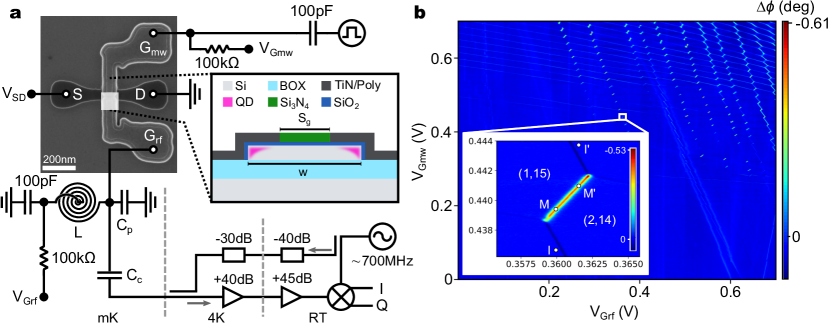
Figure 1a shows a scanning electron microscopy (SEM) micrograph of an -type CMOS split-gate transistor fabricated on a 300 mm silicon-on-insulator (SOI) wafer similar to the device presented here. The inset of Figure 1a presents the cross-section of the silicon channel of the transistor, which has a height , a width and is separated from the Si substrate, which we hold at , by a 145 nm SiO2 buried oxide (BOX). On top and separated from the channel by of SiO2, there is a pair of face-to-face gate electrodes (G and G), which have gate length and are split from each other by . The space between and around the gates is covered by 34 nm-wide Si3N4 spacers which help separate the highly--type-doped source (S) and drain (D) contacts from the central part of the intrinsic channel. The channel region below G is lighty Bi doped with an average of Bi dopant under the area of the G gate. By increasing the electrostatic potential of G and G, electrons accumulate in the corners of the channel thus forming two quantum dots, QD and QD, in parallel between the source and drain, which have controllable electron occupancies (see inset of Figure 1a) Voisin et al. (2015). Electrons can be drawn in to the quantum dots from the S and D reservoirs, which we hold at .
We control and read the electron configuration of the DQD via the setup presented in Figure 1a. The microwave gate (G) is connected to a DC line () and a high frequency line through a bias tee. The other gate, the reflectometry gate (G), is connected to a DC line () and, in parallel, to a lumped-element LC resonant circuit comprised of a superconducting NbN planar spiral inductor as well as the parasitic capacitance to ground, . At , the resonance frequency of the resonator is ; however when increasing the magnetic field, the kinetic inductance of the superconducting spiral inductor increases, leading to shifts in according to , where is the magnetic field dependent inductance of the spiral inductor, is the coupling capacitance and is the state-dependent device capacitance. We drive the resonator close to resonance with a frequency and power at the input of the resonator in the range of to . The signal reflected from the resonant circuit is amplified by at and by further at room temperature, where it is subsequently homodyne IQ demodulated and low-pass filtered, thus allowing measurement of the phase shift of the reflected signal, . Variations in phase, where is the loaded quality factor, arise due to changes in device capacitance that occur, for example, when single electrons tunnel cyclically between QDs, or between a QD and a reservoir, because of the influence of the rf drive Mizuta et al. (2017).
We present the charge stability diagram in Figure 1b111The charge stability diagram in Figure 1b is stitched together by 49 individual diagrams, each of dimension 0.1 V by 0.1 V obtained by measuring the phase response as a function of the voltages and . The hexagon-like features in the diagram confirm the presence of a DQD in the Si channel and the lines of non-zero phase shift indicate regions of charge bistability. The short lines with positive slope indicate electron tunneling between dots whereas the quasi-vertical (quasi-horizontal) lines correspond to regions where QD (QD) exchanges an electron with the source/drain reservoirs. We note a larger voltage period of the lines in with respect to , which we attribute to a misalignment of nm in the placement of the gates on the Si channel in which G overlaps the channel more so than G. The increased elongation and the rounding of the corners of the hexagons at larger gate voltages indicate an increased tunnel coupling between the dots Wiel et al. (2002). Gate-based reflectometry readout enables us to count the number of electrons down to the first ones by counting voltage shifts in the vertical and horizontal lines (see Supporting Information S1). The inset of Figure 1b shows the region of the charge stability diagram around the even-parity interdot charge transition (ICT) between the (1,15) and (2,14) DQD charge configurations. Here in refers to the electron occupancy of QD while refers to the electron occupancy of QD. The tunneling between the two dots results in a change of device capacitance given by the quantum capacitance of the system, which in the slow relaxation limit can be described by the expression Mizuta et al. (2017)
| (1) |
where is the electron charge, is the difference between the capacitive coupling ratio of G to QD and QD, is the eigenenergy of the many-particle state , and is the probability of the state being occupied. The points I, I′, M, and M′ in the inset indicate the initialisation and measurement points used for pulsing experiments described later in this letter. In the following, we focus on the region and ICT shown in the inset of Figure 1b.
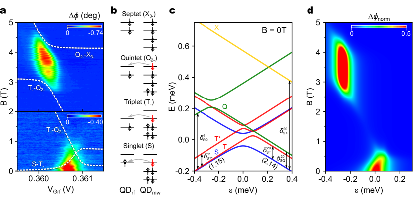
In order to study the spin physics of the multi-electron DQD defined in this device, and in particular the ICT shown in Figure 1b, we perform a dispersive magnetospectroscopy study by measuring the line-trace intersecting the ICT at V while increasing the magnetic field, , which is applied in-plane with the device and at an angle to the nanowire. To account for the magnetic field dependent inductance , which changes significantly for , the magnetospectroscopy study is split into two measurements as presented in Figure 2a, where is adjusted accordingly for to . The measurements show that the signal seen at in Figure 1b disappears when , and that a new signal at slightly lower appears at and eventually disappears again at .
The signal at arises from tunneling between the anti-crossing singlet states S(1,15) and S(2,14) as given by Equation (1) and as sketched in the lower panel of Figure 2b. The curvature of the anti-crossing singlet states is apparent from their calculated eigenenergies that appear in blue in Figure 2c as function of energy detuning between dots , where V in this experiment. When is increased, excited states with a non-zero spin angular momentum projection onto the direction of , , will Zeeman-split according to , where is the Landé -factor and is the Bohr magneton. A Zeeman-split state, for example the triplet T- with illustrated in Figure 2b, can therefore become the ground state at sufficiently large . In this scenario, the tunneling between T(1,1)- and S(2,0)-like states – T-(1,15) and S(2,14) here – is forbidden by the Pauli exclusion principle Lai et al. (2011); Petta et al. (2005); Maurand et al. (2016); West et al. (2019), thereby leading to Pauli spin blockade: the ICT signal disappears because T shows no curvature at detuning and thus makes no contribution to . One may therefore initially be led to believe that the lack of signal from in Figure 2a is due to singlet-triplet spin blockade and that the signal at arises from the curvature of the T-(1,15)-T-(2,14) anti-crossing Betz et al. (2015); House et al. (2015); Landig et al. (2019). As we explain below, this is however not the case.
In the lower part of Figure 2a, we note that as is increased from 0 to 0.8 T, the ICT signal decreases in intensity asymmetrically from the left. The reduction of signal can be ascribed to the lowering of T- below the singlet ground state. This is illustrated by the dashed white line labelled S-T- in Figure 2a, which tracks the position of the S-T- crossing above which T- becomes the new ground state of the system as previously explained (see Supporting Information S2 for energy diagrams similar to Figure 2c at non-zero magnetic fields). Because the signal of the singlet disappears at lower first, the anti-crossing between T-(1,15) and T-(2,14) states must appear at larger gate voltage. For that reason, the signal in the region cannot arise from triplet tunneling but, as we demonstrate below, instead comes from hybridised quintet spin states (). By closer inspection of the region (Supporting Information S3), we do however identify the signal of the T- anti-crossing. This signal overlaps that of the low-field singlet because the singlet-triplet splitting of this system, , is small relative to the tunnel coupling of the singlet states, , thereby making the two signals difficult to discern. The triplet signal is accompanied by a second peak (Supporting Information S3) arising from the tunneling between an excited triplet, T*-(1,15), and T-(2,14) as illustrated with the red eigenenergies in Figure 2c. This additional triplet anti-crossing explains the extension of the low-field ICT signal beyond the S-T- crossing line.
As we increase the magnetic field further, the triplet signals vanish at about , but at a new signal starts appearing as displayed in the upper part of Figure 2a. We attribute this new signal to the anti-crossing between the lowest Zeeman-split quintet states Q2-(2,14) and Q2-(1,15) with (green lines in Figure 2c), which have four electrons aligned with the external magnetic field, as illustrated in Figure 2b. Consequently, the Q2- state experiences twice the Zeeman splitting in comparison to the T- and T*- states, thereby explaining how the quintet state can become a ground state at a sufficiently large magnetic field (Supporting Figure S2c). Just as the T- state blocks the singlet state at lower fields, the low energy Q2- state now crosses the T- state as shown with the dashed white line labeled T--Q2- in Figure 2a, causing triplet-quintet spin blockade in the range. We note that the discontinuity of the fitted dashed T--Q2- line at T may be due to changes in charge in the peripheral environment of the DQD between measurements. Increasing the magnetic field beyond results in a six electron X3- septet state with and (top panel of Figure 2b and yellow line in Figure 2c), which experiences thrice the Zeeman splitting compared to the triplet, to move below the Q2- state and become the new ground state (Supporting Figure S2d). This generates yet another region of spin blockade as seen in the upper part of Figure 2a. Magnetospectrocopy measurements with features similar to those presented here were obtained for a neighbouring even-parity ICT with 2 fewer electrons on QD as well as in another similar device (Supporting Information S4).
From the measurements presented in Figure 2a, we compile quantitative information about the energy spectrum of the DQD, which we use to produce Figure 2c showing the singlet (blue), triplet (red), quintet (green) and septet (yellow) states at . We obtain from the slopes of the asymmetrically vanishing ICT signals (dashed lines in Figure 2a). We get the minimum energy separation between states with same total spin number – the tunnel couplings – from the full width at half maximum (FWHM) of the signals at a fixed (Supporting Information S5) and thus extract eV for the singlet at T, eV for the quintet at T and estimate eV and eV at T for the T-(1,15)-T-(2,14) and the T*-(1,15)-T-(2,14) tunnel coupling, respectively. Finally, from the signal position on the axis and the magnetic fields at which the different spin blockades occur, we extract the energy splitting between states in the (2,14) and (1,15) configurations, which we reference for simplicity as (2,0) and (1,1), respectively. We get the singlet-triplet splitting on the (2,0) side, eV, the singlet-triplet∗ splitting on the (1,1) side, eV, the singlet-quintet splitting on the (1,1) side eV and the (2,0) side eV and lastly the singlet-septet splitting on the (2,0) side eV. The smallest splittings, and , may be associated with valley splittings, while the others involve combinations of valley and orbital excitations in QD. Using the parameters introduced above, we build the multi-spin Hamiltonian of the system (Supporting Information S6) and extract the eigenenergies, , as plotted in Figure 2c. Using the expression for and the magnetic field dependence of the eigenenergies, we obtain the simulated magnetospectrocopy map of Figure 2d for which we included a finite electron temperature . The good match between data and simulation confirms our understanding of the DQD energy spectrum and thereby opens up for the possibility of probing the dynamical properties of the high-spin states accessible in this DQD.
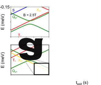
Spin relaxation time is an important metric as it ultimately limits coherence and determines the minimum readout time to achieve high fidelity spin readoutKloeffel and Loss (2013). The spin relaxation in silicon has been measured for single spins Morello et al. (2010), singlet-triplet systems West et al. (2019), hybrid qubits Shi et al. (2012), and hole spins Crippa et al. (2019); van der Heijden et al. (2018). In the following we explore spin relaxation from spin quintet states. To determine the relaxation time of the Q2- state, we first set at which point the DQD is under triplet-quintet spin blockade. Figure 3a shows the energy levels at as simulated based on the parameters extracted from magnetospectroscopy. At this field, the Q2- anti-crossing at meV lies at energies slightly higher than the energy of the T- state, however at sufficiently large , Q2-(2,14) is the ground state. To probe the Q2- anti-crossing, we therefore apply a 50% duty cycle square wave voltage pulse to G that is initialised (I) from the (1,14) configuration and then pulsed to the measurement point (M) on the ICT as seen in the inset of Figure 1b. When crossing the (1,14)-(2,14) charge transition, an electron is loaded into QD at a rate , given that the transition produces a measurable phase shift in the resonator response Gonzalez-Zalba et al. (2015). We set the rise/fall time of the pulse to 10 ns, much slower than the tunnelling time, such that the system is initialised in the energetically favoured Q2-(2,14) state. The quintet state is subsequently followed through adiabatic passage to the Q2- anticrossing (point M), as illustrated in the inset of Figure 3a, causing a non-thermal occupation probability. Finally, the electron is unloaded and the system reset via the reverse procedure.
To measure , we wait for a time at point M, during which the Q2- state relaxes to the T- state with a characteristic relaxation time as indicated in the inset of Figure 3a. When spending very little time () at the measurement point of the pulse sequence, the probability that the Q2- state relaxes tends to 0, which leads to lifting of the spin blockade and generation of the ICT phase shift signal from the curvature of the Q2- state according to Equation (1). Contrarily if , the probability that the Q2- state relaxes to the non-curving T- state tends to 1 and we therefore no longer measure the ICT signal.
We repeat the pulse sequence described above times for various and with the rf drive continuously on, thus measuring the average of the voltage region around the Q2- anti-crossing. From fitting the line-trace to , where and is the detuning and the tunnel coupling of the quintet anti-crossing, respectively, and are constants Mizuta et al. (2017), the maximum phase shift is extracted. In order to obtain the Q2--T- relaxation time, is then plotted as a function of and fitted to a single exponential decay, , where are constants, as shown in Figure 3b, whereby we find .
Setting the magnetic field to , we now study the quintet in the region of quintet-septet spin blockade, illustrated in Figure 3c which shows the simulated energy levels at this magnetic field. While similar to the lower field triplet-quintet scenario, here the Q2- state is the ground state at , i.e. in the (1,15) configuration, rather than at meV. This change affects the pulsing scheme required to determine the relaxation time. The voltage pulses on G are modified accordingly, starting instead from the (2,15) state (I′) in order to initialise the system in the energetically favoured Q2-(1,15) before moving via adiabatic passage to the measurement point (M′) as shown in the insets of Figures 1b and 3c. As in the quintet-triplet case, is extracted from the ICT phase response and fitted against a single exponential decay, , shown in orange in Figure 3d, which results in a Q2--X3- relaxation time that is comparable to . While there are no other reported quintet relaxation timescales to benchmark these results to, it is about three orders of magnitude smaller than previously reported relaxation times in singlet-triplet DQD systems West et al. (2019); Pakkiam et al. (2018); Prance et al. (2012). The mechanism explaining the faster quintet relaxation may be subject for further studies.
In summary, we have demonstrated the formation of a tunnel-coupled DQD in the channel of a split-gate silicon transistor. By embedding the device in an LC electrical resonator and performing gate-based dispersive sensing, we have determined the charge state of the DQD down to the last electron. By tuning to the (1,15)-(2,14) interdot charge transition and studying the quantum capacitance of the system as a function of magnetic field, we have found evidence of multi-particle high-spin states not studied before, namely electron spin quintets () and spin septets (). From the magnetospectroscopy measurements, we determined the energy spectrum as a function of energy detuning between dots as well as the coupling energy between states with equal spin numbers. Additionally, we have developed a model to describe the magnetic field dependence of the dispersive response based on the multi-state quantum capacitance of the system. The model reproduces the experimental results well and generally provides a tool for understanding dispersive signal in systems with a complex spin configuration. Finally, non-equilibrium studies measured under spin blockade and presented here demonstrate a typical quintet relaxation time, , at the hybridisation point. Overall, our results provide a way to reconstruct the energy spectrum of complex spin systems and open up for the possibility of using CMOS quantum dots as a tuneable test bed for studying the interactions and dynamics of high-spin systems.
This research has received funding from the European Union’s Horizon 2020 Research and Innovation Programme under grant agreement No 688539 (http://mos-quito.eu). T.L. acknowledges support from the EPSRC Cambridge NanoDTC, EP/L015978/1. M.F.G.Z. acknowledges support from the Royal Society and the Winton Programme for the Physics of Sustainability. Y.M.N. and J.L. acknowledge support from the French National Research Agency (ANR project MAQSi).
References
- Tayebjee et al. (2017) M. J. Y. Tayebjee, S. N. Sanders, E. Kumarasamy, L. M. Campos, M. Y. Sfeir, and D. R. McCamey, Nature Physics 13, 182 (2017).
- Smith and Michl (2010) M. B. Smith and J. Michl, Chemical reviews 110, 6891 (2010).
- Kim et al. (2018) H. Kim, K. Wang, Y. Nakajima, R. Hu, S. Ziemak, P. Syers, L. Wang, H. Hodovanets, J. D. Denlinger, P. M. R. Brydon, et al., Science advances 4, eaao4513 (2018).
- Yu and Liu (2018) J. Yu and C.-X. Liu, Physical Review B 98, 104514 (2018).
- Swart et al. (2004) M. Swart, A. R. Groenhof, A. W. Ehlers, and K. Lammertsma, The Journal of Physical Chemistry A 108, 5479 (2004).
- Chapyshev et al. (2000) S. V. Chapyshev, R. Walton, J. A. Sanborn, and P. M. Lahti, Journal of the American Chemical Society 122, 1580 (2000).
- Teki et al. (2001) Y. Teki, S. Miyamoto, M. Nakatsuji, and Y. Miura, Journal of the American Chemical Society 123, 294 (2001).
- Malinowski et al. (2018) F. K. Malinowski, F. Martins, T. B. Smith, S. D. Bartlett, A. C. Doherty, P. D. Nissen, S. Fallahi, G. C. Gardner, M. J. Manfra, C. M. Marcus, et al., Physical Review X 8, 11045 (2018).
- Chen et al. (2017) B.-B. Chen, B.-C. Wang, G. Cao, H.-O. Li, M. Xiao, G.-C. Guo, H.-W. Jiang, X. Hu, and G.-P. Guo, Physical Review B 95, 35408 (2017).
- van der Heijden et al. (2018) J. van der Heijden, T. Kobayashi, M. G. House, J. Salfi, S. Barraud, R. Laviéville, M. Y. Simmons, and S. Rogge, Science advances 4, eaat9199 (2018).
- Leon et al. (2019) R. C. C. Leon, C. H. Yang, J. C. C. Hwang, J. C. Lemyre, T. Tanttu, W. Huang, K. W. Chan, K. Y. Tan, F. E. Hudson, K. M. Itoh, et al., arXiv:1902.01550 (2019).
- Tyryshkin et al. (2012) A. M. Tyryshkin, S. Tojo, J. J. L. Morton, H. Riemann, N. V. Abrosimov, P. Becker, H.-J. Pohl, T. Schenkel, M. L. W. Thewalt, K. M. Itoh, et al., Nature materials 11, 143 (2012).
- Saeedi et al. (2013) K. Saeedi, S. Simmons, J. Z. Salvail, P. Dluhy, H. Riemann, N. V. Abrosimov, P. Becker, H.-J. Pohl, J. J. L. Morton, and M. L. W. Thewalt, Science 342, 830 (2013).
- Maurand et al. (2016) R. Maurand, X. Jehl, D. Kotekar-Patil, A. Corna, H. Bohuslavskyi, R. Laviéville, L. Hutin, S. Barraud, M. Vinet, M. Sanquer, et al., Nature communications 7, 13575 (2016).
- Veldhorst et al. (2017) M. Veldhorst, H. G. J. Eenink, C. H. Yang, and A. S. Dzurak, Nature communications 8, 1766 (2017).
- Crippa et al. (2019) A. Crippa, R. Ezzouch, A. Aprá, A. Amisse, L. Houtin, B. Bertrand, M. Vinet, M. Urdampilleta, T. Meunier, M. Sanquer, et al., Nature communications 10, 2776 (2019).
- Yoneda et al. (2018) J. Yoneda, K. Takeda, T. Otsuka, T. Nakajima, M. R. Delbecq, G. Allison, T. Honda, T. Kodera, S. Oda, Y. Hoshi, et al., Nature nanotechnology 13, 102 (2018).
- Huang et al. (2019) W. Huang, C. H. Yang, K. W. Chan, T. Tanttu, B. Hensen, R. C. C. Leon, M. A. Fogarty, J. C. C. Hwang, F. E. Hudson, K. M. Itoh, et al., Nature 569, 532 (2019).
- Watson et al. (2018) T. F. Watson, S. G. Philips, E. Kawakami, D. R. Ward, P. Scarlino, M. Veldhorst, D. E. Savage, M. G. Lagally, M. Friesen, S. N. Coppersmith, M. A. Eriksson, and L. M. Vandersypen, Nature 555, 633 (2018).
- Morello et al. (2010) A. Morello, J. J. Pla, F. A. Zwanenburg, K. W. Chan, K. Y. Tan, H. Huebl, M. Möttönen, C. D. Nugroho, C. Yang, J. A. Van Donkelaar, A. D. Alves, D. N. Jamieson, C. C. Escott, L. C. Hollenberg, R. G. Clark, and A. S. Dzurak, Nature 467, 687 (2010).
- Schroer et al. (2012) M. D. Schroer, M. Jung, K. D. Petersson, and J. R. Petta, Physical review letters 109, 166804 (2012).
- Yang et al. (2019) C. H. Yang, R. C. C. Leon, J. C. C. Hwang, A. Saraiva, T. Tanttu, W. Huang, J. C. Lemyre, K. W. Chan, K. Y. Tan, F. E. Hudson, et al., arXiv:1902.09126 (2019).
- Zhao et al. (2018) R. Zhao, T. Tanttu, K. Y. Tan, B. Hensen, K. W. Chan, J. C. C. Hwang, R. C. C. Leon, C. H. Yang, W. Gilbert, F. E. Hudson, et al., arXiv:1812.08347 (2018).
- Kloeffel and Loss (2013) C. Kloeffel and D. Loss, Annu. Rev. Condens. Matter Phys. 4, 51 (2013).
- Fogarty et al. (2018) M. A. Fogarty, K. W. Chan, B. Hensen, W. Huang, T. Tanttu, C. H. Yang, A. Laucht, M. Veldhorst, F. E. Hudson, K. M. Itoh, et al., Nature communications 9, 4370 (2018).
- Harvey-Collard et al. (2018) P. Harvey-Collard, B. D’Anjou, M. Rudolph, N. Tobias Jacobson, J. Dominguez, G. A. Eyck, J. R. Wendt, T. Pluym, M. P. Lilly, W. A. Coish, M. Pioro-Ladrière, and M. S. Carroll, Physical Review X 8, 021046 (2018).
- Betz et al. (2015) A. C. Betz, R. Wacquez, M. Vinet, X. Jehl, A. L. Saraiva, M. Sanquer, A. J. Ferguson, and M. F. Gonzalez-Zalba, Nano letters 15, 4622 (2015).
- Culcer et al. (2012) D. Culcer, A. L. Saraiva, B. Koiller, X. Hu, and S. D. Sarma, Physical review letters 108, 126804 (2012).
- Petersson et al. (2010) K. D. Petersson, C. G. Smith, D. Anderson, P. Atkinson, G. A. C. Jones, and D. A. Ritchie, Nano letters 10, 2789 (2010).
- Colless et al. (2013) J. I. Colless, A. C. Mahoney, J. M. Hornibrook, A. C. Doherty, H. Lu, A. C. Gossard, and D. J. Reilly, Physical review letters 110, 46805 (2013).
- Ahmed et al. (2018) I. Ahmed, J. A. Haigh, S. Schaal, S. Barraud, Y. Zhu, C.-m. Lee, M. Amado, J. W. A. Robinson, A. Rossi, J. J. L. Morton, and M. F. Gonzalez-Zalba, Phys. Rev. Applied 10, 14018 (2018).
- Voisin et al. (2015) B. Voisin, R. Maurand, S. Barraud, M. Vinet, X. Jehl, M. Sanquer, J. Renard, and S. De Franceschi, Nano letters 16, 88 (2015).
- Mizuta et al. (2017) R. Mizuta, R. M. Otxoa, A. C. Betz, and M. F. Gonzalez-Zalba, Physical Review B 95, 45414 (2017).
- Note (1) The charge stability diagram in Figure 1b is stitched together by 49 individual diagrams, each of dimension 0.1 V by 0.1 V.
- Wiel et al. (2002) W. V. D. Wiel, S. D. Franceschi, J. Elzerman, T. Fujisawa, S. Tarucha, and L. Kouwenhoven, Reviews of Modern Physics 75, 1 (2002).
- Lai et al. (2011) N. S. Lai, W. H. Lim, C. H. Yang, F. A. Zwanenburg, W. A. Coish, F. Qassemi, A. Morello, and A. S. Dzurak, Scientific Reports 1, 1 (2011).
- Petta et al. (2005) J. R. Petta, A. C. Johnson, J. M. Taylor, E. A. Laird, A. Yacoby, M. D. Lukin, C. M. Marcus, M. P. Hanson, and A. C. Gossard, Science 309, 2180 (2005).
- West et al. (2019) A. West, B. Hensen, A. Jouan, T. Tanttu, C.-H. Yang, A. Rossi, M. F. Gonzalez-Zalba, F. Hudson, A. Morello, D. J. Reilly, et al., Nature nanotechnology 14, 437 (2019).
- House et al. (2015) M. G. House, T. Kobayashi, B. Weber, S. J. Hile, T. F. Watson, J. Van Der Heijden, S. Rogge, and M. Y. Simmons, Nature communications 6, 1 (2015).
- Landig et al. (2019) A. J. Landig, J. V. Koski, P. Scarlino, C. Reichl, W. Wegscheider, A. Wallraff, K. Ensslin, and T. Ihn, Physical Review Letters 122, 213601 (2019).
- Shi et al. (2012) Z. Shi, C. B. Simmons, J. R. Prance, J. K. Gamble, T. S. Koh, Y.-P. Shim, X. Hu, D. E. Savage, M. G. Lagally, M. A. Eriksson, et al., Physical review letters 108, 140503 (2012).
- Gonzalez-Zalba et al. (2015) M. F. Gonzalez-Zalba, S. Barraud, A. J. Ferguson, and A. C. Betz, Nature communications 6, 6084 (2015).
- Pakkiam et al. (2018) P. Pakkiam, A. V. Timofeev, M. G. House, M. R. Hogg, T. Kobayashi, M. Koch, S. Rogge, and M. Y. Simmons, Physical Review X 8, 1 (2018), arXiv:1809.01802 .
- Prance et al. (2012) J. R. Prance, Z. Shi, C. B. Simmons, D. E. Savage, M. G. Lagally, L. R. Schreiber, L. M. K. Vandersypen, M. Friesen, R. Joynt, S. N. Coppersmith, et al., Physical Review Letters 108, 46808 (2012).