Topological flat bands without magic angles in massive twisted bilayer graphenes
Abstract
Twisted bilayer graphene (TBG) hosts nearly flat bands with narrow bandwidths of a few meV at certain magic twist angles. Here we show that in twisted gapped Dirac material bilayers, or massive twisted bilayer graphenes (MTBG), isolated nearly flat bands below a threshold bandwidth are expected for continuous small twist angles up to a critical depending on the flatness of the original bands and the interlayer coupling strength. Narrow bandwidths of 30 meV are expected for for twisted Dirac materials with intrinsic gaps of eV that finds realization in monolayers of gapped transition metal dichalcogenides (TMDC), silicon carbide (SiC) among others, and even narrower bandwidths in hexagonal boron nitride (BN) whose gaps are eV, while twisted graphene systems with smaller gaps of a few tens of meV, e.g. due to alignment with hexagonal boron nitride, show vestiges of the magic angles behavior in the bandwidth evolution. The phase diagram of finite valley Chern numbers of the isolated moire bands expands with increasing difference between the sublattice selective interlayer tunneling parameters. The valley contrasting circular dichroism for interband optical transitions is constructive near and destructive near alignments and can be tuned through electric field and gate driven polarization of the mini-valleys. Combining massive Dirac materials with various intrinsic gaps, Fermi velocities, interlayer tunneling strengths suggests optimistic prospects of increasing and achieving correlated states with large effective interaction versus bandwidth ratios.
I Introduction
The field of atomically thin two dimensional (2D) materials has seen an enormous progress over the last fifteen years since the successful experiments identifying the massless Dirac cones in graphene Novoselov et al. (2004); Geim and Grigorieva (2013); Zhang et al. (2005). In recent years the research directions have shifted towards tailoring the electronic structure of 2D material heterojunctions by selective material control and stacking arrangement Young and Kim (2009); Gong et al. (2014); Huang et al. (2014); Duan et al. (2014). New families of hexagonal 2D materials beyond graphene including group IV layered materials Drummond et al. (2012); Vogt et al. (2012); Liu et al. (2011a); Ni et al. (2011); Dávila et al. (2014); Matthes et al. (2013), semiconducting and metallic transition metal dichalcogenides (TMDC) Wilson and Yoffe (1969); Mattheiss (1973); Wang et al. (2012a); Xu et al. (2014) expand the list of the so called Dirac materials whose relevant band structure near the Fermi level is located at the and Dirac points at the Brillouin zone corners. Modifications in the stacking arrangements are expected to introduce significant changes in the electronic structures of 2D materials assemblies. One prototypical example is the twisted bilayer graphene Hass et al. (2008); Miller et al. (2009, 2010); Sadowski et al. (2006); De Heer et al. (2010); Brihuega et al. (2012); Ohta et al. (2012); Lopes dos Santos et al. (2012, 2007); Shallcross et al. (2010, 2008); Landgraf et al. (2013); Shallcross et al. (2013); Bistritzer and MacDonald (2011); Moon and Koshino (2013, 2012); Jung et al. (2014); San-Jose et al. (2012); San-Jose and Prada (2013); Stauber et al. (2013); Bistritzer and MacDonald (2010); Wang et al. (2012b); Schmidt et al. (2014); Carr et al. (2018); Koshino et al. (2018); Kang and Vafek (2019); Tarnopolsky et al. (2019); Po et al. (2019) where the relative rotation of one of the layers gives rise to new features in the electronic structure such as van Hove singularities and secondary Dirac cones Luican et al. (2011); Li et al. (2010) that can be understood based on the associated moire bands Bistritzer and MacDonald (2011); Lopes dos Santos et al. (2012); Jung et al. (2014); Wong et al. (2015); Kerelsky et al. ; Choi et al. (2019). Observations of superconductivity Cao et al. (2018a); Yankowitz et al. (2019); Cao et al. (2019) and correlated phases Cao et al. (2018b); Kim et al. (2017); Sharpe et al. (2019) in twisted bilayer graphene have sparked a renewed interest in searching the properties of twisted bilayer graphene and flat bands in other types of twisted 2D materials. New proposals for flat bands in hybrid heterostructures include transition metal dichalcogenides Wu et al. (2018); Naik and Jain (2018); Naik et al. (2019); Pan et al. (2018), hexagonal boron nitride bilayers Xian et al. (2019); Zhao et al. (2019), van der Waals patterned dielectric superlattices Shi et al. (2019), multilayer graphene systems such as twisted bi-bilayer graphene Chebrolu et al. (2019); Zhang et al. (2019a); Liu et al. (2019a), and rhombohedral trilayer graphene on hexagonal boron nitride where gate tunable correlated and superconducting phases have been observed experimentally Chen et al. (2019a, b). When the Dirac material layers are gapped by applying vertical electric fields Chittari et al. (2019); Chebrolu et al. (2019); Liu et al. (2019b); Lee et al. (2019); Shen et al. (2019); Choi and Choi (2019); Koshino (2019) or when the gaps are already open like in BN/BN bilayers Xian et al. (2019), the bandwidths remained reduced continuously for small twist angles rather than only at a discrete set of magic angles like in twisted bilayer graphene Bistritzer and MacDonald (2011). In this work we investigate the behavior of the low energy bands bandwidth for different massive twisted bilayer graphene (MTBG) Hamiltonians and find that nearly flat bands below a threshold bandwidth can be achieved for a continuous range of twist angles up to a critical angle that increases with the band gap size and with the reduction of the Fermi velocity. Our study indicates that low energy nearly flat bands can be expected in the vicinity of band edges for small enough twist angles in a variety of gapped materials including semiconducting TMDC, silicon carbide (SiC), and hexagonal boron nitride (BN) and other 2D materials twisted bilayers when they can be appropriately modeled by gapped Dirac Hamiltonians. This flexibility in the twist angle choice should enormously facilitate the preparation of twistronics devices to tailor the flat bands. Furthermore, we calculated the associated topological valley Chern numbers phase diagram that can lead to spontaneous quantum Hall phases in the absence of magnetic fields Haldane (1988); Kane and Mele (2005); Nandkishore and Levitov (2010); Jung et al. (2011); Zhang et al. (2011) when the degeneracy of these bands are lifted under the effects of spin or valley polarising time reversal symmetry breaking perturbations Chittari et al. (2019); Zhang et al. (2019a); Chen et al. (2019c), and whose signatures have been measured in recent experiments Sharpe et al. (2019); Serlin et al. (2019); Chen et al. (2019c). The interband transition and circular dichroism in twisted gapped Dirac materials is studied as a function of twist angle, electric fields and stacking alignment between the layers to illustrate the tunability of the optical properties in the system.
The manuscript is organized as follows. We present in Sec. II the theoretical details of the Hamiltonian model used in Sec. III to analyze the bandwidth dependence as a function of Hamiltonian parameters. In Sec. IV we discuss the analytical solutions of the eigenvalues at the symmetry points of the moire Brillouin zone. Then in Sec. V we discuss the valley Chern number phase diagram, and in Sec. VI the circular dichroism of the interband transition oscillator strengths before we close the manuscript in Sec. VII with the summary and discussions.
II Twisted Gapped Dirac Hamiltonian model
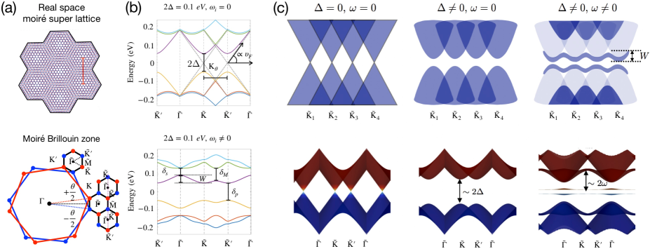
The twisted gapped Dirac materials systems we consider are described based on the conventional assumption of the moire bands theory that the interlayer tunneling strength varies slowly with respect to the 2D position on an atomic scale Bistritzer and MacDonald (2011); Wallbank et al. (2013); Lopes dos Santos et al. (2012); Jung et al. (2014). Our continuum Hamiltonian shares the same periodicity of the moire pattern and we employ the Bloch’s theorem to formulate the effective low energy electronic structure in the moire Brillouin zone it defines, see Fig. 1(a). The moire bands theory used in graphene on graphene (G/G) and subsequent extension for more general material combinations including graphene on hexagonal boron nitride (G/BN) have been discussed in Ref. Jung et al. (2014), where a recipe is proposed to inform the model Hamiltonian parameters from first principles calculations from the crystal Hamiltonian that goes beyond the two center approximation for the interatomic interactions. The associated continuum models are generalized to include additional diagonal and off-diagonal moire pattern terms to the Bistritzer-MacDonald model resulting in:
| (1) |
where the bottom and top layers are twisted symmetrically in opposite senses to preserve the orientation of the moire pattern and therefore of the moire Brillouin zone (mBZ)
| (2) |
where is centered at the point of each rotating layer, the index distinguishes which layer. The triangular moire patterns for the scalar and vector potentials are given by
| (3) | |||||
| (4) | |||||
| (5) |
where that respects the triangular symmetry is defined in terms of with the six first shell moire reciprocal lattice vectors generated rotating successively by an angle of Jung et al. (2014, 2017) is equivalent to a sum of three cosines with alternating first shell G-vectors Wu et al. (2019)
| (6) |
The operator accounts for the rotation of the electrons in momentum space through small phase differences between the top and bottom layers and is responsible for the chiral circular dichroism observed in TBG for twist angles in opposite senses Kim et al. (2016); Morell et al. (2017). For the analysis presented in this work we neglect these small additional phases because their effect is generally small and we can obtain electron-hole symmetric bands some simple interlayer tunneling values.
We use the conventional form of the interlayer tunneling in the small angle approximation distinguishing the different sublattice resolved tunneling terms Bistritzer and MacDonald (2011); Jung et al. (2014)
| (7) |
where the three vectors and are proportional to twist angle and is the Brillouin zone corner length of the Dirac material of lattice constant where for graphene and for MoS2. The interlayer coupling matrices between the two rotated adjacent layers are generically given by
| (8) |
where we distinguish three different , and interlayer sublattice tunneling obtained averaging over all possible stacking configurations and assume for simplicity that they are real values. The convention taken here for the matrices assume an initial AA stacking configuration Jung et al. (2014) and differs by a phase factor with respect to the initial AB stacking Bistritzer and MacDonald (2011). We use a similar naming convention for the AA, AB and BA local stacking arrangements of the unit cell atoms also for the 60∘ or equivalently 180∘ degrees alignment of the layers where the two sublattice atoms of the top layer are switched regardless of choice for the rotation center.
The moire band Hamiltonians were modeled from existing parameters in the literature for G/G Chittari et al. (2019); Chebrolu et al. (2019), TMDC/TMDC Xiao et al. (2012); Wu et al. (2019), and informed from first-principles calculation for SiC/SiC and BN/BN for this work. The parameter fitting procedure follows closely those of Ref. Jung et al. (2014) while the details for SiC/SiC are presented in appendix A.
| Monolayer parameters and interlayer tunneling | ||||||
| Bilayer | a (Å) | |||||
| G/G (rigid) | 2.46 | 2.6 | 0.098 | - | ||
| G/G (relaxed) | 2.46 | 3.1 | 0.098 | 0.12 | 0.098 | - |
| MoS2 /WS2 | 3.195 | 1.1/1.37 | 0.01 | 1.66/1.79 | ||
| MoS2 /MoS2 | 3.193 | 1.1 | 0.01 | 1.66 | ||
| WS2 /WS2 | 3.197 | 1.37 | 0.01 | 1.79 | ||
| BN/BN (0∘) | 2.48 | 2.5 | 0.178 | 0.147 | 0.078 | 4.58 |
| BN/BN (60∘) | 2.48 | 2.5 | 0.208 | 0.148 | 0.078 | 4.59 |
| SiC/SiC | 3.06 | 1.7 | 0.165 | 0.413 | 0.063 | 2.383 |
| WSe2 /WSe2 | 3.32 | 1.261 | 0.0011 | 0.0 | 0.0097 | 1.2 |
| Intralayer moire patterns | ||||||
| Coefficients | A-A | B-B | A′-A′ | B′-B′ | A-B | A′-B′ |
| BN/BN (0∘) | ||||||
| 2.333 | 2.247 | 2.333 | 2.247 | - | - | |
| 0.0180 | 0.0098 | 0.0180 | 0.0098 | 0.0044 | 0.0044 | |
| 67.9 | 77.9 | 67.9 | 77.9 | 145 | 145 | |
| BN/BN (60∘) | ||||||
| 2.368 | 2.222 | 2.222 | 2.368 | - | - | |
| 0.0027 | 0.0026 | 0.0026 | 0.0027 | 0.0059 | 0.0059 | |
| 85.8 | 72.91 | 72.707 | 85.8 | 120.12 | 120.12 | |
| SiC/SiC | ||||||
| 1.319 | 1.064 | 1.319 | 1.064 | - | - | |
| 0.0426 | 0.0085 | 0.0426 | 0.0085 | 0.0 | 0.0 | |
| 42.71 | 26.56 | 42.71 | 26.56 | 0.0 | 0.0 | |
| WSe2/WSe2 | ||||||
| 1.2 | 1.2 | - | - | |||
| 0.0068 | 0.0068 | 0.0 | 0.0 | |||
| 89.7 | 91.0 | 0.0 | 0.0 | |||
III Bandwidth phase diagram in twisted gapped Dirac materials
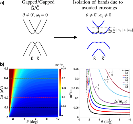
Here we show that the low energy moire bands in twisted gapped Dirac materials have narrow bandwidths for a continuous range of twist angles in contrast to the discrete set of magic angles in twisted bilayer graphene. Specifically we show that the bandwidth of the low energy moire bands remain extremely narrow below a threshold value up to critical twist angle of which scales almost linearly with the intrinsic band gap and interlayer tunneling , and is inversely proportional to the Fermi velocity . Hints of this behavior were observed in ABC-trilayer graphene on BN under a perpendicular electric field Chittari et al. (2019), in the evolution of bandwidth in twisted BN/BN systems Xian et al. (2019); Zhao et al. (2019), and more recently in twisted double bilayer graphene subject to electric fields Liu et al. (2019b); Lee et al. (2019); Shen et al. (2019); Choi and Choi (2019); Koshino (2019), and twisted transition metal dichalcogenides Wu et al. (2018); Naik and Jain (2018); Naik et al. (2019); Pan et al. (2018). To understand the behavior of the moire bands in our MTBG systems it is useful to review the behavior of the discrete set of magic angles in the Bistritzer-MacDonald model of twisted bilayer graphene where the band structure scaling parameter relating the interlayer coupling strength with the twist angle and the Fermi velocity was used to identify the angles where the Fermi velocity vanishes at the Dirac point Bistritzer and MacDonald (2011). This scaling parameter summarizes the relationship between the system parameters indicating that flat bands can be achieved more easily for greater interlayer coupling , and for smaller Fermi velocities and twist angles . Fig. 1(b) illustrates how these parameters defining can affect the band structures. For instance, finite interlayer tunneling terms introduce coherence between the moire bands opening a secondary gap at which together with the primary gap at allows the formation of isolated Chern bands, see Fig. 1(c). The bandwidth can be defined as the energy difference of the band energy at and the band edge at or , and we can define as the avoided gap at the point located between and .
The linear relationship between and suggested by the structure of for the first magic angle was confirmed by explicit bandwidth calculations that numerically satisfy the relationship for the magic angle both in twisted bilayer graphene Chittari et al. (2019) and for the first magic angle corresponding to in the minimal model of twisted bi-bilayer graphene Chebrolu et al. (2019) confirming that the magic twist angles should increase together with interlayer coupling strength as expected from this scaling relation Chittari et al. (2019); Carr et al. (2018). These magic angles were defined as the values that give rise to bandwidth local minima rather than the angles where the effective Fermi velocity vanishes at the -points of the mBZ Bistritzer and MacDonald (2011) since this definition would become ambiguous in twisted bi-bilayers or gapped Dirac materials whose band edges already have zero Fermi velocity.
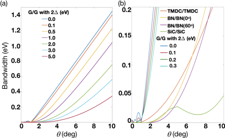
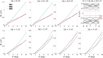
The bandwidths generally increase with twist angles and decrease with the band gap as shown in Fig. 2, where we have represented the evolution of the bandwidth with twist angle of gapped graphene with a finite mass term. Similar evolutions of are shown also for other gapped Dirac materials that we modeled through other system parameters listed in Table 1 that aims to capture the behavior of the band edges near the -points, or the (macro)valleys of single layers, of a variety of materials comprising twisted bilayers of gapped G, TMDCs including MoS2 and WS2, SiC, BN.
While increase in bandwidth is expected for large twist angles, a non monotonic behavior can be present depending on the details of the Hamiltonian like in our example of SiC/SiC low energy valence band. In all the materials considered showing monotonic increase of with twist angle we observe that the critical twist angle required to achieve a given bandwidth increases for increasing and and decreasing . Hence, we can normally expect that the bandwidth will remain smaller than for all the angles below the critical . A plausible alternative definition of not used here would be the ratio between the Coulomb repulsion and bandwidth. The relationship between and the system parameters is captured for the twisted gapped Dirac bilayer model with a single tunneling parameter through
| (9) |
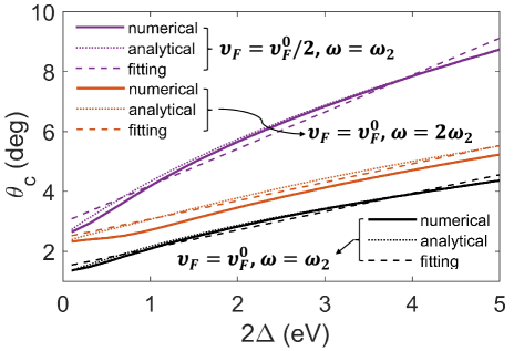
where we use the dimensionless constants of , , , and is the nearest neighbor hopping amplitude in a honeycomb lattice that can be related with the Fermi velocity of the Dirac Hamiltonian through . The Eq. (9) shows the interdependence of with the system parameters , , and can be used to determine the critical angle associated to a specific critical bandwidth that we aim for. The Fig. 3 compares numerically calculated with approximate analytical forms discussed in Sec. IV and confirms the interdependence of the parameters in Eq. (9) relating the twist angle , interlayer coupling strength , the Fermi velocity of each layer, and the staggered potential between the sublattices within each layer that gives rise to the intrinsic gaps.
Our calculations show that the MTBG is advantageous for the generation of flat bands in comparison to TBG for two important reasons. First there is no need to aim for a specific magic twist angle to achieve narrow bandwidths when the gaps are sufficiently large, and second the gap opening allows to achieve flat bands for larger twist angles than in TBG where the structural stability of the moire pattern is greater Jung et al. (2015). Flat bands for larger twist angles implies in turn that stronger correlated phases are in principle achievable because the moire Coulomb interactions are roughly proportional to twist angle, where is the electron charge and is the lattice constant of the individual triangular lattice.
This MTBG model is a well defined model that can illustrate the behavior of various gapped Dirac material combinations both for the small and large gap limits. In the small gap limit a massive graphene layer has experimental realization in graphene aligned with hexagonal boron nitride (G/BN) Hunt et al. (2013); Wang et al. (2016); Woods et al. (2014); Jung et al. (2015); Kim et al. (2018); Kindermann et al. (2012); San-Jose et al. (2014); Yankowitz et al. (2016) that opens a band gap of meV or larger depending on sample preparation methods. Likewise band gaps of the order of few tens of meV are expected in silicene, germanene layers due to intrinsic spin-orbit coupling effects Liu et al. (2011b). The massive twisted bilayer graphenes can also serve as approximate models for other gapped Dirac materials such as SiC, hBN and TMDC Xiao et al. (2012) type triangular lattice 2D materials.
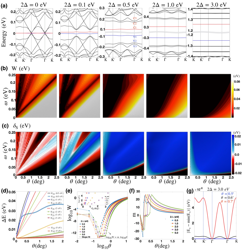
The evolution of MTBG flat bands in massive twisted bilayer graphenes are clearly summarized in Fig. 4 where we show the resulting band structure, bandwidth and isolation gaps expected as a function of gap size , twist angle , and interlayer coupling for a wide range of parameters that can describe several twisted gapped Dirac materials. In Fig. 4(a) we show the band structure from electron-hole symmetrized Bistritzer-MacDonald model of twisted bilayer graphene that uses a single interlayer tunneling parameter and removes the rotation phases in each graphene layer. The results are obtained for a fixed twist angle and variable gap sizes between till eV where it is clearly shown that finite values of intralayer gaps creates a band gap at the primary Dirac point and also generates a secondary isolation gap whose magnitude increases progressively as becomes larger. It is important that both primary and secondary gaps remain finite in order to isolate the low energy bands and allow a stronger effective Coulomb interaction. When intralayer band gaps are large enough the primary and secondary gaps open simultaneously in a larger system parameter space of and . In the limit of small intralayer gaps of a few tens of meV like in aligned G/BN structures this reduced bandwidth region concentrate around the magic angle lines in the parameter space and thus we can still identify vestiges of the zero gap limit. A progressive increase in the gap size alters the phase diagram of the bandwidth in vs space merging the discrete traces of magic angle lines into a larger area in the phase diagram expanding the parameter space where we can find finite secondary gaps . This broadening of the parameter space leads to the disappearance of the discrete magic angles and gives rise to a continuous range of twist angles with reduced bandwidth when the band gaps are larger than a few hundreds of meV. We have typically explored twist angles from to for , where the tildes indicates the presence of gaps, and up to for larger gap materials, and interlayer coupling values that span between 0 to 0.25 eV, over two times larger than eV in bilayer graphene. For models with unequal tunneling values we define and keep the same fixed ratios of and when we scale the strenght of interlayer coupling for the different materials listed in Table 1 using for rigid , for relaxed , / = 0.83, / = 1.89 for BN/BN(0∘), / = 0.71, / = 1.89 for BN/BN(60∘), and / = 2.5, / = 6.5 for SiC/SiC.
An additional effect we observe from the gap increase is the progressive flattening of the higher energy bands, where we observe bandwidths smaller than a few meVs giving rise to a practically discrete set of atomic or quantum dot like energy spectra when individual layer primary gaps assume values of a few eVs for twist angles around . The twist angle dependence of these quasi-flat higher energy bands follows an approximately linear evolution with and is summarized in Fig. 4(d), where we show differences in the energy levels of meV between the lowest two energy levels, and smaller than meV for the energy spacing between the second and third levels when the twist angles are changed by . The bandwidth evolution for the higher energy bands in MTBG for different gap sizes are shown in appendix C. Remarkable flattening of the bands down to numerical values of eV are represented in Fig. 4(e)-(g). For small twist angles they are widened rapidly with increasing twist angle as with powers as large as 25 that gradually reduces with increasing twist angles approaching the limiting behavior of hyperbolic bands in the small gap limit. This rapid compression in for sufficiently small implies that the density of states around the average band energy of a given band
| (10) |
will roughly be proportional to the moire Brillouin zone area that scales with and is inversely proportional to the bandwidth in the absence of van Hove singularities. According to this estimate we expect nearly flat bands prone to Coulomb interaction driven ordered phases whose bandwidths evolve with twist angle as even if we do not have divergences associated to saddle points in the Fermi surface. The rapid enhancement in the joint density of states between the flat bands, when not limited by the broadening due to disorder, will more than compensate the decrease of the oscillator strengths in the flat bands to enhance the optical absorption in the system.
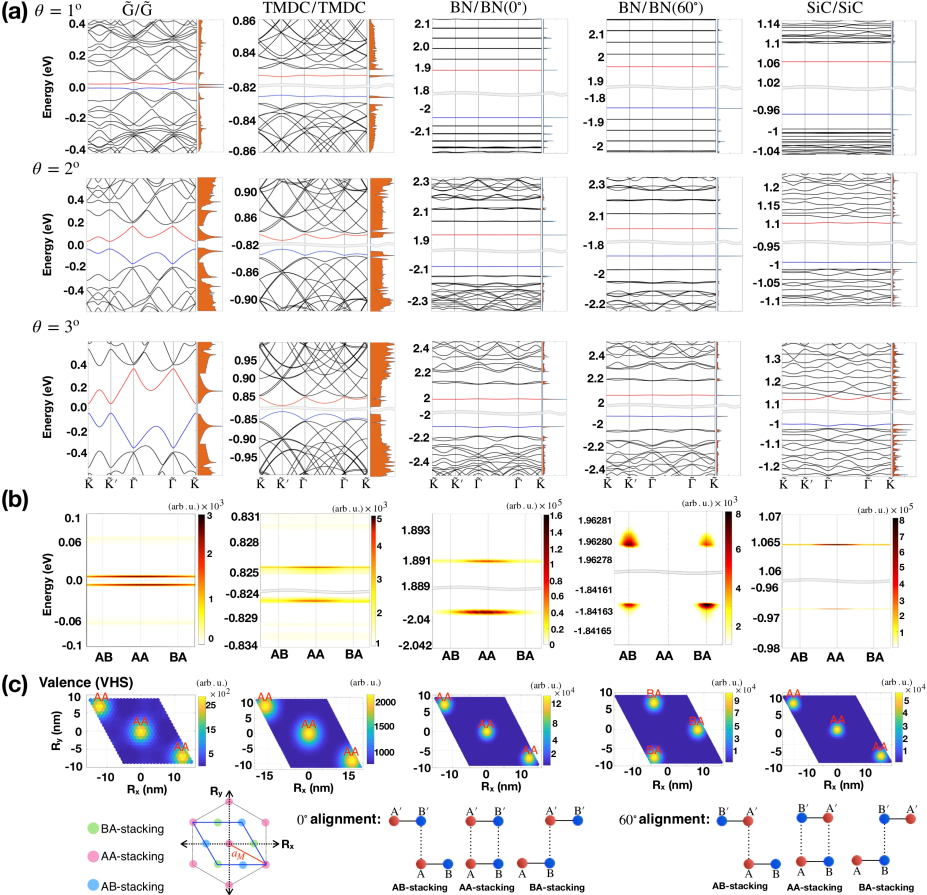
The twist angle dependence of the electronic structure and DOS for a variety of materials and the associated density of states (DOS) and local density of states (LDOS) are shown in Fig. 5. We notice that when the primary gap near charge neutrality and the secondary isolation gap are simultaneously present the low energy flat bands are isolated from the neighboring higher energy bands and they can acquire a well defined integer valley Chern number Song et al. (2015); Zhang et al. (2019a); Chittari et al. (2019). As we commented earlier on, the electronic structure of large gap MTBG like in BN/BN bilayers whose individual layer gaps are above several eV shows that higher energy bands are also flattened. These high energy flatband states should be accessible through carrier gating techniques for marginally twisted BN bilayers when the electron densities for each moire band and the interband energy spacing between the contiguous flat bands are reduced.
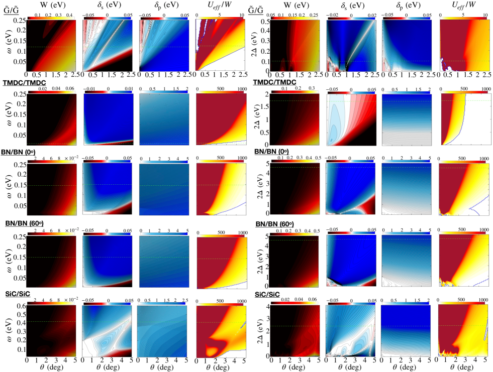
A different perspective for the interdependence of bandwidth and system parameters in is seen in the parameter space of and in Fig. 6 where we can observe how the traces of the magic angles are erased for 20.2 eV, consistent with the observations in Fig. 2. Apart from the obliteration of the magic angles, the increase in the single layer bandgap gives rise to a nonzero primary gap , generally smaller than , that lifts the band degeneracy at charge neutrality, and opens a secondary isolation gap even when all three interlayer tunneling parameters are the same. We also observe that the increase of interlayer coupling allows to achieve flat bands at greater twist angles as noted in earlier works Chittari et al. (2019); Carr et al. (2018), suggesting that we can look for materials with stronger interlayer coupling as a pathway to achieve stronger correlated phases due to reduced moire pattern period, as evidenced in our SiC/SiC proposal.
Since the primary gap near the charge neutrality and the secondary gap near the point of the mBZ are important factors that can influence the onset of interaction-driven phase ordering, we have studied these isolation gaps in the parameter space of (, 2) and (, ) for all the massive systems listed in Table. 1. Greater band isolation should reduce screening due to electrons in neighboring bands and therefore strengthen the effective Coulomb interactions. We have represented in Fig. 6 the ratio obtained using the screened Coulomb potential Chebrolu et al. (2019)
| (11) |
where the moire length is , and the Debye length uses the 2D density of states that assumes a value proportional to the band overlap ratio when , where is the heaviside step function. We use the relative dielectric constant , and there are four valley-spin degenerate electrons per moire unit cell area for each filled moire band. The phase diagram for of gapped systems in the parameter space of and shows that for small gaps we can still identify traces of the magic angle lines present in gapless tBG Chittari et al. (2019) together with the suppression of the bandwidth and isolation through and gaps, whereas in large gapped systems we can find a larger continuous parameter space of narrow band widths with large ratio.
IV Analytical expressions of , , and .
Analytical expressions of the physical quantities relevant for describing the flat bands including the bandwidth , the primary gap , the isolation gap and avoided gap can be obtained from the eigenvalues at the different symmetry points in the moire Brillouin zone by solving the truncated moire bands Hamiltonian in the first shell approximation Jung et al. (2014); Bistritzer and MacDonald (2011). The electronic structure of twisted Dirac bilayers results from the coherence between the constituent layers, ranging from the perturbative weakly coupled regime for large twist angles to progressively stronger coupling at small twist angles where multiple momenta scattering is required in order to capture the electronic structure of the coupled bilayer. The truncation for the Hamiltonian that we use is therefore just appropriate to describe the systems with large enough twist angles where the narrow bandwidth starts to become more dispersive. For the analysis in this section we consider the minimal model of the gapped Dirac cones connected by the interlayer tunnelings matrices given in Eq. (8) and preserve the convenient electron-hole symmetry eliminating the rotation phases phases that accompany the twists in each layer and present our analysis for the conduction flat bands which can be equally applied for the valence bands. We assume for simplicity in the tunneling terms and allow for a different which enhances the isolation gap . We denote by the conduction band. By using and the band energies of the first and second conduction bands we can define
| (12) | |||||
| (13) | |||||
| (14) | |||||
| (15) |
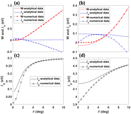
following the properties of the moire bands shown in Fig. 1(b). The conduction band minimum of the flat band is always at the point, whereas the maximum always happens at the point. Consequently, the bandwidth of the conduction band () and the primary gap () are obtained from and . The minimum of the second conduction band is for small , so the isolation gap is correctly given by Eq. (13) for sufficiently small twist angles when is a minimum. For large twist angles, the second conduction band minimum moves away from the point starting to deviate from Eq. (13) but this estimate can still be useful for discriminating the isolation of the flat bands. A comparison of our analytical expressions against numerically obtained is offered in the appendix B. The avoided gap or the eigenenergies at give additional information about the band structure at the zone boundary of the moire Brillouin zone.
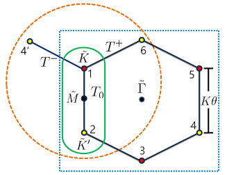
In Fig. 7 we show the schematic of high-symmetry points in the mBZ which are used to obtain the analytical expressions, where the and odd and even indices are used to label the gapped Dirac cones of the bottom and top layers respectively. The eignvalues are evaluated from an 8-bands model consisting of four gapped Dirac cones in the dashed brown circle, while the are calculated from a 12-bands model which includes six gapped Dirac cones inside the dotted blue square. The energies for the avoided gaps can be obtained from a 4-bands model of two intersecting gapped Dirac cones within the green oval in Fig. 7. The interlayer tunneling among the contiguous cones are , as given in Eq. (8), and here we limit the discussions to the case of . The displacement between the contiguous Dirac points is , where is the distance between to in the single layer BZ. The analytical resolution of the eigen energies and eigenvectors for moire systems should also be useful to understand the topological properties of the band structures from point group symmetry considerations Fang et al. (2012).
IV.1 Calculation of from an model
We consider an 8-bands model including only the four gapped Dirac cones inside the dashed circle given in Fig. 7 to derive the analytical form of . Our approach is similar to the scheme used in Ref. Bistritzer and MacDonald (2011) to calculate the renormalized Dirac-point band velocity in TBG. The 8-bands model Hamiltonian connecting one gapped Dirac cone with three surrounding gapped cones reads
| (16) |
whose diagonal blocks are gapped Dirac Hamiltonians
| (17) |
where is the mBZ momentum, and is the momentum orientation with respect to the axis. The is the gapped Dirac cone index, so determines the center of the -th Dirac cone. The eigenstate consists of four two-component spinors . We find that at the point, the spinors for the first conduction band always follows the relations , , where is a diagonal matrix given by
| (18) |
The discussions for the valence bands are closely similar and they are shown in appendix B. Consequently, the first conduction band energy at the point is given by
| (19) |
where
For , the twisted gapped Dirac bilayer model given in Eq. (1) preserves electron-hole symmetry in the absence of the aforementioned rotation phases, and the lowest band edges reside at the point Hence the resulting analytical expression of the primary gap is
| (20) |
where is given by Eq. (19).
Due to the electron-hole symmetry, the first valence band energy at point is available from Eq. (19). For the valence band states at we can define the two-component spinors for the model in a similar way to what we have done for the conduction band. The eigenstate consists of four two-component spinors , and the first valence band always follows the relations , , where is a diagonal matrix given by
| (21) |
IV.2 Analytical expression of
The eigenenergy at the point can be calculated from the Hamiltonian consisting of six gapped Dirac cones inside the blue dotted square in Fig. 7. The interlayer tunneling between contiguous gapped Dirac cones are given by the , matrices, and the Hamiltonian reads
| (22) | ||||
The eigenstate consists of six two-component spinors , and we find that the spinors always follow the relations , , , , and is a diagonal matrix
| (23) |
where only have three different combinations, which are , , and . The eigenvalues for the valence bands at the point have electron-hole symmetry and are related to the conduction band energies through , and . Likewise the valence band eigenvectors can be defined with the same spinor structure for the conduction bands but using the phases that follow from this electron-hole symmetry of the eigenenergies. For each (1,2,3), the eigenenergy problem is then changed to solving a quartic equation
| (24) |
For the three sets, the coefficients in Eq. (24) become different, and by solving the equation for each one can get 4 roots, among which only one root is useful in our calculation. Hence for three s we obtain three different energy eigenvalues and denote them as whose exact expressions are given in appendix B and here we use the following approximations
| (25) | ||||
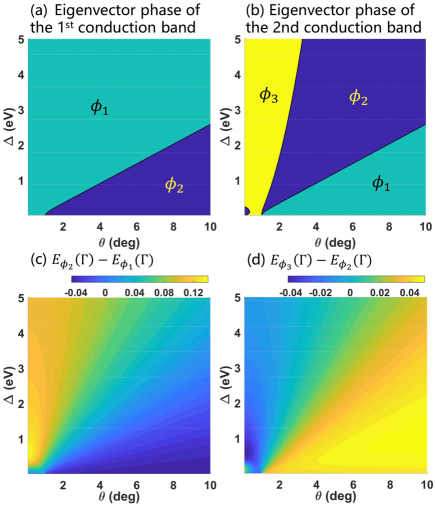
We represent in Fig. 8 the parameters that determine the eigenstates of the first and second conduction flat bands. In this figure the first conduction band energy is given by either or , while the second conduction band energy is given by either , or depending on the Hamiltonian parameters and . Consequently, the expressions of the bandwidth and the isolation gap are
| (26) | ||||
IV.3 Analytical models for
The moire bands in reciprocal space are repeated periodically by the moire reciprocal lattice vectors . The coherence between the two overlapping bands of the rotated layers can be approximated in the simplest perturbative limit by a four by four Hamiltonian neglecting all but the smallest momenta coupling equivalent to two interacting gapped Dirac cones where the bands would otherwise intersect between and as illustrated in Fig. 9.
| (27) |
The energy eigenvalue at the -point can be obtained by diagonalizing Eq. (27). For the simplest case when , the two conduction band energies at the -point are given by
| (28) |
where from which we can conclude that the energy difference for the avoided gap is
| (29) |
If , the -point conduction band energy eigenvalues are
| (30) | ||||
In the limit of large , one can approximate to obtain
| (31) |
which further simplifies to
| (32) |
if we assume , and .
The above Hamiltonian and associated solutions can be further simplified to a model in the limit of large band gaps thanks to the almost perfect sublattice polarization of the conduction and valence bands. In this limit, we can build a two by two Hamiltonian that couples two conduction or two valence mutually coupled through a single tunneling parameter , and in the presence of an interlayer potential difference we have
| (33) |
that couples through the two conduction or valence band edges arising from the top and bottom layers whose bands represented along the line that connects the two shifted moire zone -points are shown in Fig. 9 for . By denoting for the band edges we obtain the following eigenvalues
| (34) |
Keeping in mind that at the point the avoided gap reduces to
| (35) |
The effective mass of the electron given by
| (36) |
has an analytical approximation near given by,
| (37) |
that reduces to the point value of a single gapped Dirac cone in the limit of large twist angles Xiao et al. (2007). The numerical from the low energy bands are represented in Fig. 9 as a function of gap and twist angle.
V Topological flat bands and valley Chern numbers
Isolated bands in the moire Brillouin zone can develop integer valley Chern numbers different from zero depending on the details of the Hamiltonian Song et al. (2015); Chittari et al. (2019); Zhang et al. (2019b). A finite charge Hall conductivity will develop when the valley degeneracy is lifted by valley polarization in an otherwise time reversal invariant system Zhang et al. (2019a); Chittari et al. (2019). This type of selective valley and spin filling mechanisms have been proposed to underlie the observed ferromagnetism and anomalous Hall effects in twisted bilayer graphene aligned with a boron nitride substrate Sharpe et al. (2019); Serlin et al. (2019), and the ordered phases in twisted double bilayer graphene Liu et al. (2019b); Lee et al. (2019); Shen et al. (2019); Choi and Choi (2019). On a closely related topic for our work, opposite valley Chern numbers of have been proposed in twisted bilayer graphene with a small gap of 15 meV in one of the layers aligned with the hexagonal boron nitride substrate Bultinck et al. (2019); Zhang et al. (2019a) while Coulomb interactions could trigger low energy bands even in the absence of substrate effects MacDonald (2019). Analogous valley Chern bands due to intralayer moire patterns have also been proposed in twisted semiconducting TMDC Wu et al. (2019). Recent observations of quantized anomalous Hall conductance at zero magnetic field in TBG Serlin et al. (2019) or non quantized orbital moments Sharpe et al. (2019), and at small magnetic fields of T in ABC trilayer graphene on hexagonal boron nitride in the presence of electric field induced gaps of meV Chen et al. (2019c) suggest optimistic prospects of finding exotic zero magnetic field quantum Hall states when the device qualities are sufficiently improved.
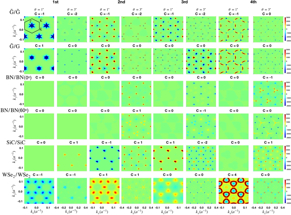
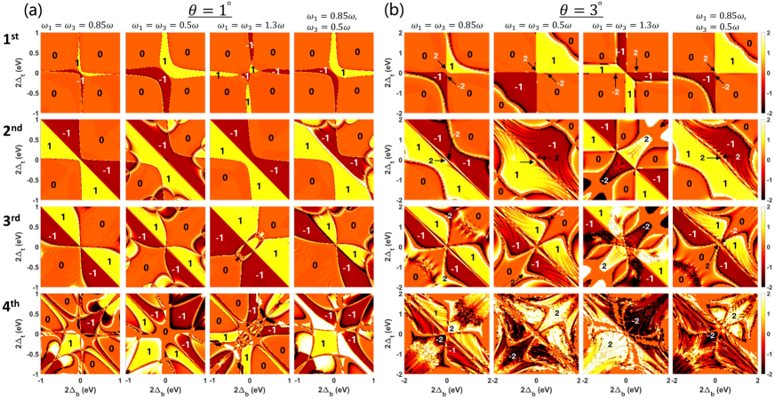
In the following we show the valley Chern number phase diagram expected in MTBG for different sets of system parameters , , , (1,2,3) and for the first four conduction bands near charge neutrality expanding beyond the parameter region studied in earlier related work Zhang et al. (2019a); Bultinck et al. (2019); Chittari et al. (2019), see appendix D for a similar phase diagram and Berry curvature plots of the valence bands. We calculate numerically the valley Chern numbers through the standard formula Xiao et al. (2010)
| (38) |
where is the valley index, using the Berry curvature of the band
| (39) |
where and are the eigenenergies and eigenvectors. The maxima of Berry curvatures as illustrated in Fig. 10 often concentrate around the different symmetry points of the mBZ at , or , and near the moire Brillouin zone boundaries where the avoided gaps are formed. Some general conclusions we can anticipate from our calculations of the Chern number phase diagram of twisted gapped Dirac bilayers are that (i) the conduction and valence bands remain topologically trivial if and their relative magnitudes sensitively contribute in determining the phase space of topological bands, (ii) as the band gap of the system becomes larger we need to increase the twist angle to turn the lowest band into a Chern band, (iii) the intralayer moire patterns contribute in the determination of the Chern number phase diagram, and (iv) small values of interlayer bias comparable in magnitude with the interlayer tunneling can lead to higher energy band crossings and changes in Chern number, as was seen in models of TMDC consisting of intralayer moire potentials Wu et al. (2018).
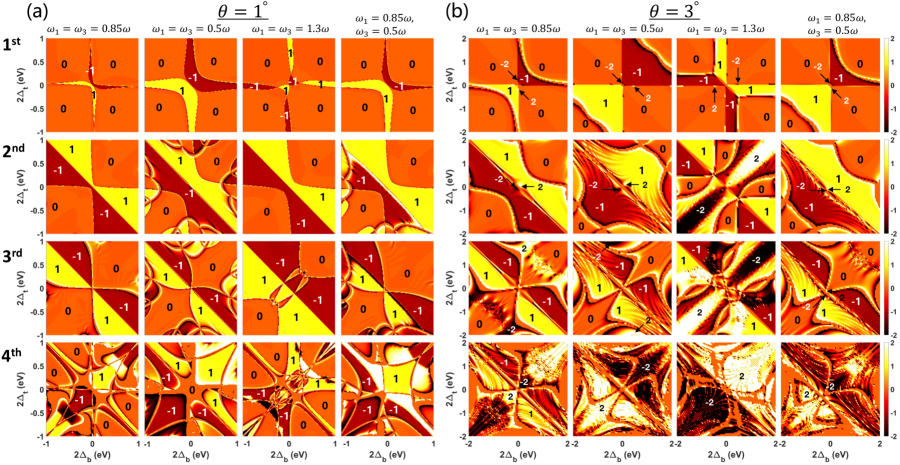
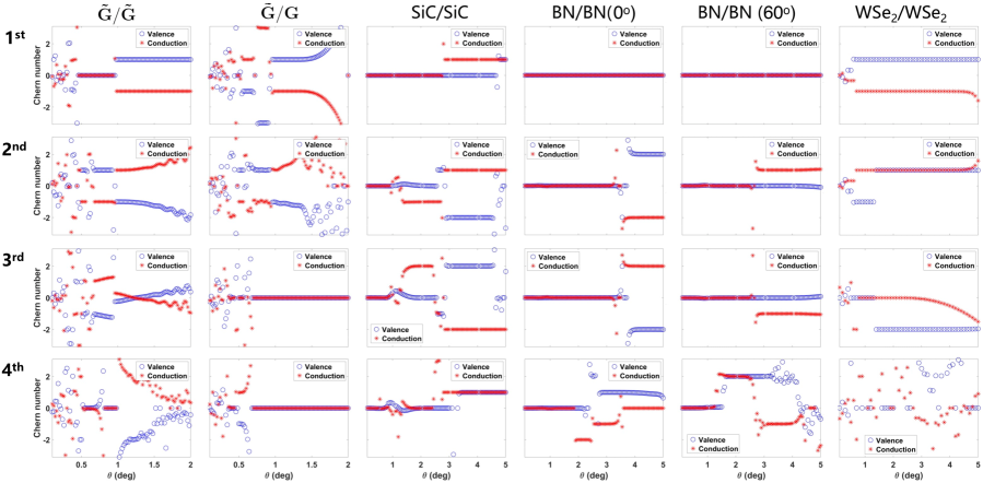
In Fig. 11 we represent the Chern number phase diagrams for the first four conduction bands of two twisted gapped Dirac materials as a function of the gap magnitudes. The phase diagrams for the valence bands are similar to that of conduction bands with opposite Chern numbers except for electron-hole symmetry breaking and they are presented in appendix D. We have shown the phase diagrams corresponding to different twist angles of and in Fig. 11’s (a) and (b) panels respectively where we find that shortening of the moire period by increasing can turn the low energy bands into Chern bands in large gap systems. This behavior can be explained if we consider that an increase in twist angles enlarges the mBZ area and prevents the Berry curvature weights at the low energy bands to be pushed to higher energies. Sensitive changes of Chern number as a function of gap magnitude found for large twist angles and high energy bands indicate the complex avoided crossing structure at higher energies. We have listed in each column the Chern bands phase diagram for same parameter as in graphene and use different interlayer tunneling terms , and variable gap values () of the bottom (top) layer. In the first and second columns we show the results for the interlayer tunneling parameters of and . As noted earlier, if we choose the values of (1,2,3) to be identical, both conduction and valence bands are trivial in the , phase space, but if the diagonal tunneling terms become distinct from the off-diagonal the integer valley Chern number emerges in two belt regions that become wider as the difference between and increases. Hence, the low energy Chern bands are possible only when there are at least two different values coupling different sublattices in Eq. (8), and a sufficiently small finite mass term in at least one of the layers. The nontrivial Chern band parameter region is generally larger in space when the differences in the tunneling parameters are also large, as we can verify comparing and columns, and we have an intermediate situation for where we additionally include a difference between the diagonal hopping parameters . The former case is closely related with the experimental situation of TBG where one layer is aligned with BN. When the maximum allowed gap is 50 meV before the level becomes trivial, whereas if the maximum allowed to preserve a topological band is about 140 meV. A qualitatively different phase diagram is found when when the diagonal tunneling elements become larger than the off-diagonal interlayer terms, while we still require small enough mass terms to preserve a Chern band. However, even when the mass terms are as large as a few eVs it is possible to find Chern bands for large enough twist angles and higher energy bands. The valley Chern bands appear even for small twist angles in WSe2/WSe2 system modeled mainly through intralayer moire patterns. We have represented in Fig. 12 the twist angle dependence of the Chern numbers for several massive twisted bilayer graphene systems that we modeled from the parameters in Table 1. For small band gaps we find nonzero valley Chern numbers for the lowest energy bands in a wide range of twist angles in the limit of small band gaps. When the intralayer band gaps are larger we notice a tendency for higher energy bands to acquire finite Chern numbers for sufficiently large twist angles for interlayer tunneling dominated moire pattern systems like SiC/SiC and BN/BN bilayers.
VI Valley contrasting optical transitions
Numerous optical experiments for semiconducting transition metal dichalcogenides have verified optical dichroism in broken inversion symmetry single layer materials Zhang et al. (2018); Yao et al. (2008); Cao et al. (2018c) associated with the chirality of the layers in twisted multilayer systems Kim et al. (2016); Morell et al. (2017); Stauber et al. (2018). In the simplest picture, circular dichroism is expected in gapped Dirac materials due to valley contrasting orbital moments associated with the Berry curvatures at the band edges for circularly polarized dipole optical interband transitions involving angular momentum changes of Yao et al. (2008), and leading to selection rules of the form for the promotion of angular momentum excitons in -chiral gapped Dirac systems Zhang et al. (2018); Cao et al. (2018c). Here we investigate how in a gapped twisted bilayer graphene system the circular dichroism for the interband optical transitions are modified going from the decoupled layers limit consisting of two independent gapped Dirac Hamiltonian layers to two coupled gapped Dirac Hamiltonians leading to strongly hybridizing flatbands. In our models this crossover in behavior can be achieved either by changing the rotation angle between the bilayers or by modifying the interlayer coupling strength.
In a single gapped Dirac Hamiltonian model the interband optical oscillator strength for each -point for circularly polarized light is given by Yu and Cardona (2010)
| (40) |
where and is the energy difference between the and states, and we define the degree of circular polarization for each -point to be Yao et al. (2008)
| (41) |
For sake of simplicity the present analysis focuses on the strongest features of interband transitions in the dipole approximation and neglects the cross terms responsible for the optical activity due to twist angle dependent phase difference between top and bottom layers Morell et al. (2017) and the higher order terms proportional to the magnetic fields Stauber et al. (2018). Studies about the selection rules for the promotion of the excitons Zhang et al. (2018); Cao et al. (2018c) and discussions related with the moire excitons Tran et al. (2019); Seyler et al. (2019); Jin et al. (2019) for twisted gapped Dirac bilayer systems will be discussed elsewhere.
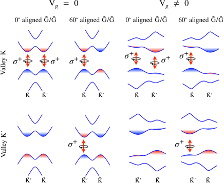
In Fig. 13 we show a schematic illustration of the band edges near each macrovalley and for twisted bilayers near and 60∘ alignments where we expect different optical responses because the band edges near and minivalleys within a macrovalley could have the same or opposite mass signs. Circular dichroism is present near alignment due to the alignment of the mass signs in each macrovalley, while near alignment the valley contrasting circular dichroism is canceled although not completely if we take into account the phases acquired due to the rotation of the layers Kim et al. (2016); Stauber et al. (2018) that should also be accounted for in our twisted gapped Dirac systems. We can see that this cancellation can also becomes nonzero when the minivalleys are polarized by the simultaneous presence of an external electric field that polarizes layer and carrier doping that shifts the Fermi level.
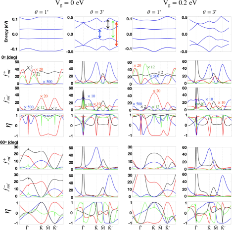
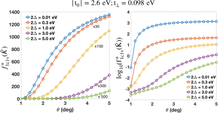
In Fig. 14 we illustrate how the interband optical transition oscillator strengths are progressively modified in twisted systems going from two weakly coupled gapped Dirac cones for large twist angles of to strongly coupled bands leading to flat band systems near . The separate representation of and allows to distinguish the sensitivity to opposite circular polarization of the states at different -points in the mBZ. In the limit of large twist angles the distribution of the oscillator strengths in the mBZ are in qualitative agreement with the expected interband transitions obtained juxtaposing two gapped Dirac cones next to each other separated by in momentum space and coupled through the interlayer tunneling parameters . For large enough twist angles and small primary gaps the interband transition oscillator strengths clearly peak around the and points in keeping with the optical properties of a single gapped Dirac Hamiltonian Xiao et al. (2007). As the twist angle is reduced and the interlayer coupling strength is enhanced we observe a progressive flattening of the bands and reduction of quasiparticle velocities that in turn results in a reduction in the oscillator strength in Eq. (40). Its evolution at the mini Dirac points represented in Fig. 15 clearly shows a superlinear suppression of the oscillator strengths as a function of the band gap and that its evolution is faster for smaller than larger twist angles. However, the almost divergent increase in the density of states in Eq. (10) due to squeezing bandwidth should increase the absorption rate as the bands become flatter until the flatness is limited by the broadening width due to disorder or temperature. This band flattening leads to smoother spread out and broad distribution of the Berry curvatures near the band edges in the mBZ. However, even in the limit of very narrow bandwidths near the oscillator strength for circularly polarized light remains predominantly centered around the minivalleys and in the mBZ resulting in a polarization function close to unity near the minivalleys. Due to the almost complete flattening of the bands we notice that an external electric field that shifts the position of the band edges near the minivalley points can introduce distortions to the band structure that are significant enough to modify the oscillator strengths.
VII summary and discussion
Recent research on twisted van der Waals materials is rapidly expanding beyond twisted bilayer graphene (TBG) to include twisted layered materials with intrinsic gaps. In this work we have identified and explained the practical advantages of twisted gapped Dirac materials over TBG for the formation of narrow bandwidth flat bands. We studied the conditions for the generation of narrow bandwidth flat bands as a function of twist angle based on the extended Bistritzer-MacDonald model of twisted bilayer graphene with a finite mass term in each one of the layers, allowing for intralayer moire patterns, and using up to three different interlayer tunneling parameters with for a more precise description of the interlayer coupling. We have identified the evolution of the low energy bandwidth () and found its dependence as a function of the band gap (), twist angles (), the Fermi velocity () and interlayer coupling (). The fitting equation Eq. (9) is expected to be valid in the parameter range where several realistic 2D material combinations lie including gapped graphene due to alignment with hexagonal boron nitride (BN), transition metal dichalcogenides (TMDC), silicon carbide (SiC), and our analysis should be valid when the band edges near the point can be described with gapped Dirac Hamiltonians.
One of the main conclusions we draw is that a finite gap in the constituent layers of the twisted gapped Dirac materials makes the generation of flat bands simpler than in TBG because already for band gaps of 250 meV the band flattening in twisted bilayers happens for a continuous range of small twist angles without requiring specific magic angles. Moreover, the larger the gaps the greater the suppression of the band width allowing to achieve narrower bands for similar twist angles, a fact that should facilitate achieving stronger effective Coulomb interactions that scales with twist angle. In moderately gapped TMDC materials or large band gap hBN materials we find that the bandwidths can remain below meV even for twist angles as large as . Stronger interlayer coupling parameters also allows to achieve narrow bandwidths for larger twist angles. In the example case of twisted SiC bilayers perturbed by relatively strong intralayer moire patterns and interlayer coupling the interplay of three unequal gave rise to valence bands with bandwidths on the order of 20 meV even for twist angles as large as 7∘, which implies a seven fold enhancement of the Coulomb interaction strength with respect to magic angle TBG based on the scale of the moire pattern periods. Our conclusions based on numerical calculations are complemented by the analytical solutions of the band eigenvalues at the symmetry points of the mBZ that provides estimates for the bandwidth as a function of the different system parameters such as twist angle, interlayer coupling and band gap.
The topological nature of the nearly flat bands in twisted gapped Dirac materials have been studied by calculating the phase diagrams for the valley Chern numbers associated to the first four conduction and valence bands. In particular, it was shown that the interlayer tunneling terms have to be different from each other for a Chern band to emerge in the limit of small intralayer band gaps like in systems of graphene on hexagonal boron nitride. The increase of twist angle in general helps to expand the phase space for the low energy valence and conduction bands to acquire a finite valley Chern number although this can effectively weaken the influence of the interlayer moire patterns and the magnitude of the isolation secondary gaps. For larger gap systems like in semiconducting TMDC or in the limit of large gap systems like hexagonal boron nitride, the lowest energy levels of a twisted bilayer remain topologically trivial but the higher bands can remain topological for large enough twist angles. These higher energy bands should be accessible either by gating techniques in devices in the small twist angle limit when the electron density per band is small, or through optical measurements. The valley contrasting circular dichroism in twisted gapped Dirac materials inherits the properties of single gapped Dirac layers whose band edges locate at the minivalley and points of the moire Brillouin zone around which maxima in the optical transition oscillator strength for circularly polarized light and Berry curvature are often found. This behavior was found to persist even in the limit where multiple atomic level like nearly flat bands were present where the traces of the original gapped Dirac cone band edges could not be clearly identified. Qualitatively distinct optical response to circularly polarized light is expected between twisted bilayer systems near and 60∘ (or equivalently 180∘) alignment where the phase winding and Berry curvature values of the bands in each minivalley could be aligned to point in the same or opposite directions respectively.
In summary, our analysis suggests optimistic prospects of finding isolated flat bands in a variety of twisted gapped Dirac materials other than twisted bilayer graphene, in particular when the original bandwidth of the building block materials are narrow to begin with, or when a strong interlayer interaction allows to access nearly flat bands for a larger range of twist angles.
Acknowledgements.
This work was supported by the Samsung Science and Technology Foundation under project no. SSTF-BA1802-06 for J. S., and from the Korean NRF grant number NRF-2016R1A2B4010105 for S. J. The 2017 Research Fund of the University of Seoul is acknowledged for J. J. Financial support for J. S. has also been granted by the National Natural Science Foundation of China (Grant No. 11604166), Zhejiang Provincial Natural Science Foundation of China (Grant No. LY19A040003) and K. C. Wong Magna Fund in Ningbo University. This work was partly performed at the Aspen Center for Physics, which is supported by National Science Foundation grant PHY-1607611.Appendix A Hamiltonian parameters fitting procedure from DFT calculations
Here we outline the methodology followed to obtain the Dirac Hamiltonian model parameters for materials involving SiC that were calculated from LDA-DFT calculations with the Perdew-Zunger parametrization Perdew and Zunger (1981). For SiC bilayers we started from the full tight-binding (FTB) model Hamiltonian for monolayer SiC using the hopping parameters extracted from the maximally localized Wannier functions by means of a two by two Hamiltonian Marzari et al. (2012) by means of a two by two Hamiltonian
| (42) |
This monolayer Hamiltonian is then used to construct the bilayer SiC Hamiltonian through
| (43) |
where, is the FTB model Hamiltonian of monolayer SiC, and T0 is the interlayer tunneling matrix as given in Eq. (8). We have determined the tunneling matrix elements that define by assuming that for large gap systems , determines the splitting in conduction, valence bands respectively, whereas controls the interaction between conduction and valence bands. When fitting the tunneling matrix elements to reproduce the DFT-bands near the -point for different standard stacking structures (AA, AB and BA) we followed the criteria that (a) the low energy bands should be parabolic at K-point so as to match with the gapped Dirac cone shaped DFT bands, (b) for all three standard SiC bilayer staking, at least four low energy bands (2-conduction,2-valence) should reproduce the DFT bands near K-point, and (c) the optimum parameters set should be unique and reproducible. With these criteria in mind the optimum tunneling parameters for AA-stacked bilayer SiC, are = 0.485 eV, = = 0, and = 0.19 eV, while for AB-stacking, = = = 0 and = 1.24 eV, and for BA-stacking = = = 0 and = 1.24 eV. The tunneling matrix elements obtained from above procedure are then averaged for the three standard stacking structures and they are = 0.165 eV, = = 0.413 eV and = 0.063 eV as listed in Table I.
Appendix B Analytical wave functions and comparison with numerical calculations
In this appendix we provide further details on the analytical solutions of the wave functions evaluated at the symmetry points. As we have discussed in the main text, only have three different combinations, which are , , and . For each (1,2,3), the eigenenergy problem is then changed to solving a quartic equation
| (44) |
which has a general formula for roots, but the roots are in quite complicated forms. For three different s, the coefficient in Eq. (44) have different values and we discuss the value and details of calculations of s below. For , the coefficients are
| (45) | ||||
If , Eq. 44 becomes a quadratic equation and one of the roots is
| (46) |
Due to the ignorance of the term, is a good approximation only for small and . The energy correction can be obtained by substituting to Eq. 44 with the coefficients given by Eq. 45, and expanding to the first order of . After a straight forward calculation, one can obtain
| (47) |
and hence
| (48) |
For case, and values for are the same as those in the case as given in Eq. 45, the only difference is that , which is with opposite sign in comparison with Eq. 45. Hence has a similar form with and is given by
| (49) |
The coefficients for case are
| (50) | ||||
The energy corresponds to at point has a simpler form
| (51) |
When , the gapped Dirac system preserves the electron-hole symmetry. We briefly discuss the energy eigenvalues the related phases for the three valence bands close to the Fermi level. As we have introduced in Section. IV. B, for each one may obtain 4 roots, which are 4 eigenenergies of the 12 by 12 Hamiltonian. The three lowest conduction band energies are given by (1,2,3), where is one of the 4 roots when the vector phases are given by . Among the other three roots for each , there exists one root which corresponds to one of the three valence bands close to the Fermi level. The valence bands energies are
| (52) | ||||
One can find that the valence band energies at the point are related to the conduction band energies as , and .
Appendix C Bandwidth evolution in higher energy bands
As noted in the main text the bandwidth of the moire energy bands are reduced when the twist angles become sufficiently small or when the intralayer gaps are increased. The narrowing of the bandwidth in the three low lying conduction or valence bands for increasing is illustrated in Fig. 17 and is also reflected in the progressive reduction of the y-axis scale. For the Hamiltonian approximation where we have used with equal and neglected the twisting phases we have electron-hole symmetry that results in equal bandwidths for the valence and conduction bands. The bandwidth compression happens most effectively for the lowest energy valence and conduction bands as the band gap is increased.
Appendix D Mass dependent Chern number phase diagram for the valence bands
The Chern number phase diagram for the valence bands shown in Fig. 18 closely resemble those of the conduction bands represented in Fig. 11 in virtue of the overall electron-hole symmetry in our model when the twist angle dependent phases are not included. The deviations in the electron-hole symmetry that distinguish the results of the valence and conduction bands stem from the use of unequal interlayer tunneling values .
References
- Novoselov et al. (2004) K. S. Novoselov, A. K. Geim, S. V. Morozov, D. Jiang, Y. Zhang, S. V. Dubonos, I. V. Grigorieva, and A. A. Firsov, science 306, 666 (2004).
- Geim and Grigorieva (2013) A. K. Geim and I. V. Grigorieva, Nature 499, 419 (2013).
- Zhang et al. (2005) Y. Zhang, Y.-W. Tan, H. L. Stormer, and P. Kim, Nature 438, 201 (2005).
- Young and Kim (2009) A. F. Young and P. Kim, Nature Physics 5, 222 (2009).
- Gong et al. (2014) Y. Gong, J. Lin, X. Wang, G. Shi, S. Lei, Z. Lin, X. Zou, G. Ye, R. Vajtai, B. I. Yakobson, et al., Nature materials 13, 1135 (2014).
- Huang et al. (2014) C. Huang, S. Wu, A. M. Sanchez, J. J. Peters, R. Beanland, J. S. Ross, P. Rivera, W. Yao, D. H. Cobden, and X. Xu, Nature materials 13, 1096 (2014).
- Duan et al. (2014) X. Duan, C. Wang, J. C. Shaw, R. Cheng, Y. Chen, H. Li, X. Wu, Y. Tang, Q. Zhang, A. Pan, et al., Nature nanotechnology 9, 1024 (2014).
- Drummond et al. (2012) N. D. Drummond, V. Zólyomi, and V. I. Fal’ko, Phys. Rev. B 85, 075423 (2012).
- Vogt et al. (2012) P. Vogt, P. De Padova, C. Quaresima, J. Avila, E. Frantzeskakis, M. C. Asensio, A. Resta, B. Ealet, and G. Le Lay, Phys. Rev. Lett. 108, 155501 (2012).
- Liu et al. (2011a) C.-C. Liu, W. Feng, and Y. Yao, Phys. Rev. Lett. 107, 076802 (2011a).
- Ni et al. (2011) Z. Ni, Q. Liu, K. Tang, J. Zheng, J. Zhou, R. Qin, Z. Gao, D. Yu, and J. Lu, Nano letters 12, 113 (2011).
- Dávila et al. (2014) M. Dávila, L. Xian, S. Cahangirov, A. Rubio, and G. Le Lay, New Journal of Physics 16, 095002 (2014).
- Matthes et al. (2013) L. Matthes, O. Pulci, and F. Bechstedt, Journal of Physics: Condensed Matter 25, 395305 (2013).
- Wilson and Yoffe (1969) J. Wilson and A. Yoffe, Advances in Physics 18, 193 (1969).
- Mattheiss (1973) L. F. Mattheiss, Phys. Rev. B 8, 3719 (1973).
- Wang et al. (2012a) Q. H. Wang, K. Kalantar-Zadeh, A. Kis, J. N. Coleman, and M. S. Strano, Nature nanotechnology 7, 699 (2012a).
- Xu et al. (2014) X. Xu, W. Yao, D. Xiao, and T. F. Heinz, Nature Physics 10, 343 (2014).
- Hass et al. (2008) J. Hass, F. Varchon, J. E. Millán-Otoya, M. Sprinkle, N. Sharma, W. A. de Heer, C. Berger, P. N. First, L. Magaud, and E. H. Conrad, Phys. Rev. Lett. 100, 125504 (2008).
- Miller et al. (2009) D. L. Miller, K. D. Kubista, G. M. Rutter, M. Ruan, W. A. de Heer, P. N. First, and J. A. Stroscio, Science 324, 924 (2009).
- Miller et al. (2010) D. L. Miller, K. D. Kubista, G. M. Rutter, M. Ruan, W. A. de Heer, P. N. First, and J. A. Stroscio, Phys. Rev. B 81, 125427 (2010).
- Sadowski et al. (2006) M. L. Sadowski, G. Martinez, M. Potemski, C. Berger, and W. A. de Heer, Phys. Rev. Lett. 97, 266405 (2006).
- De Heer et al. (2010) W. A. De Heer, C. Berger, X. Wu, M. Sprinkle, Y. Hu, M. Ruan, J. A. Stroscio, P. N. First, R. Haddon, B. Piot, et al., Journal of Physics D: Applied Physics 43, 374007 (2010).
- Brihuega et al. (2012) I. Brihuega, P. Mallet, H. González-Herrero, G. Trambly de Laissardière, M. M. Ugeda, L. Magaud, J. M. Gómez-Rodríguez, F. Ynduráin, and J.-Y. Veuillen, Phys. Rev. Lett. 109, 196802 (2012).
- Ohta et al. (2012) T. Ohta, J. T. Robinson, P. J. Feibelman, A. Bostwick, E. Rotenberg, and T. E. Beechem, Phys. Rev. Lett. 109, 186807 (2012).
- Lopes dos Santos et al. (2012) J. M. B. Lopes dos Santos, N. M. R. Peres, and A. H. Castro Neto, Phys. Rev. B 86, 155449 (2012).
- Lopes dos Santos et al. (2007) J. M. B. Lopes dos Santos, N. M. R. Peres, and A. H. Castro Neto, Phys. Rev. Lett. 99, 256802 (2007).
- Shallcross et al. (2010) S. Shallcross, S. Sharma, E. Kandelaki, and O. A. Pankratov, Phys. Rev. B 81, 165105 (2010).
- Shallcross et al. (2008) S. Shallcross, S. Sharma, and O. A. Pankratov, Phys. Rev. Lett. 101, 056803 (2008).
- Landgraf et al. (2013) W. Landgraf, S. Shallcross, K. Türschmann, D. Weckbecker, and O. Pankratov, Phys. Rev. B 87, 075433 (2013).
- Shallcross et al. (2013) S. Shallcross, S. Sharma, and O. Pankratov, Phys. Rev. B 87, 245403 (2013).
- Bistritzer and MacDonald (2011) R. Bistritzer and A. H. MacDonald, Proceedings of the National Academy of Sciences 108, 12233 (2011).
- Moon and Koshino (2013) P. Moon and M. Koshino, Phys. Rev. B 87, 205404 (2013).
- Moon and Koshino (2012) P. Moon and M. Koshino, Phys. Rev. B 85, 195458 (2012).
- Jung et al. (2014) J. Jung, A. Raoux, Z. Qiao, and A. H. MacDonald, Phys. Rev. B 89, 205414 (2014).
- San-Jose et al. (2012) P. San-Jose, J. González, and F. Guinea, Phys. Rev. Lett. 108, 216802 (2012).
- San-Jose and Prada (2013) P. San-Jose and E. Prada, Phys. Rev. B 88, 121408 (2013).
- Stauber et al. (2013) T. Stauber, P. San-Jose, and L. Brey, New Journal of Physics 15, 113050 (2013).
- Bistritzer and MacDonald (2010) R. Bistritzer and A. H. MacDonald, Phys. Rev. B 81, 245412 (2010).
- Wang et al. (2012b) Z. Wang, F. Liu, and M. Chou, Nano letters 12, 3833 (2012b).
- Schmidt et al. (2014) H. Schmidt, J. C. Rode, D. Smirnov, and R. J. Haug, Nature communications 5 (2014).
- Carr et al. (2018) S. Carr, S. Fang, P. Jarillo-Herrero, and E. Kaxiras, Phys. Rev. B 98, 085144 (2018).
- Koshino et al. (2018) M. Koshino, N. F. Q. Yuan, T. Koretsune, M. Ochi, K. Kuroki, and L. Fu, Phys. Rev. X 8, 031087 (2018).
- Kang and Vafek (2019) J. Kang and O. Vafek, Phys. Rev. Lett. 122, 246401 (2019).
- Tarnopolsky et al. (2019) G. Tarnopolsky, A. J. Kruchkov, and A. Vishwanath, Phys. Rev. Lett. 122, 106405 (2019).
- Po et al. (2019) H. C. Po, L. Zou, T. Senthil, and A. Vishwanath, Phys. Rev. B 99, 195455 (2019).
- Luican et al. (2011) A. Luican, G. Li, A. Reina, J. Kong, R. R. Nair, K. S. Novoselov, A. K. Geim, and E. Y. Andrei, Phys. Rev. Lett. 106, 126802 (2011).
- Li et al. (2010) G. Li, A. Luican, J. L. Dos Santos, A. C. Neto, A. Reina, J. Kong, and E. Andrei, Nature Physics 6, 109 (2010).
- Wong et al. (2015) D. Wong, Y. Wang, J. Jung, S. Pezzini, A. M. DaSilva, H.-Z. Tsai, H. S. Jung, R. Khajeh, Y. Kim, J. Lee, S. Kahn, S. Tollabimazraehno, H. Rasool, K. Watanabe, T. Taniguchi, A. Zettl, S. Adam, A. H. MacDonald, and M. F. Crommie, Phys. Rev. B 92, 155409 (2015).
- (49) A. Kerelsky, L. McGilly, D. M. Kennes, L. Xian, M. Yankowitz, S. Chen, K. Watanabe, T. Taniguchi, J. Hone, C. Dean, A. Rubio, and A. J. Pasupathy, arXiv:1812.08776 .
- Choi et al. (2019) Y. Choi, J. Kemmer, Y. Peng, A. Thomson, H. Arora, R. Polski, Y. Zhang, H. Ren, J. Alicea, G. Refael, et al., Nature Physics , 1 (2019).
- Cao et al. (2018a) Y. Cao, V. Fatemi, S. Fang, K. Watanabe, T. Taniguchi, E. Kaxiras, and P. Jarillo-Herrero, Nature 556, 43 (2018a).
- Yankowitz et al. (2019) M. Yankowitz, S. Chen, H. Polshyn, Y. Zhang, K. Watanabe, T. Taniguchi, D. Graf, A. F. Young, and C. R. Dean, Science 363, 1059 (2019).
- Cao et al. (2019) Y. Cao, D. Chowdhury, D. Rodan-Legrain, O. Rubies-Bigordà, K. Watanabe, T. Taniguchi, T. Senthil, and P. Jarillo-Herrero, arXiv preprint arXiv:1901.03710 (2019).
- Cao et al. (2018b) Y. Cao, V. Fatemi, A. Demir, S. Fang, S. L. Tomarken, J. Y. Luo, J. D. Sanchez-Yamagishi, K. Watanabe, T. Taniguchi, E. Kaxiras, et al., Nature 556, 80 (2018b).
- Kim et al. (2017) K. Kim, A. DaSilva, S. Huang, B. Fallahazad, S. Larentis, T. Taniguchi, K. Watanabe, B. J. LeRoy, A. H. MacDonald, and E. Tutuc, Proceedings of the National Academy of Sciences 114, 3364 (2017).
- Sharpe et al. (2019) A. L. Sharpe, E. J. Fox, A. W. Barnard, J. Finney, K. Watanabe, T. Taniguchi, M. A. Kastner, and D. Goldhaber-Gordon, Science 365, 605 (2019).
- Wu et al. (2018) F. Wu, T. Lovorn, E. Tutuc, and A. H. MacDonald, Phys. Rev. Lett. 121, 026402 (2018).
- Naik and Jain (2018) M. H. Naik and M. Jain, Phys. Rev. Lett. 121, 266401 (2018).
- Naik et al. (2019) M. H. Naik, S. Kundu, I. Maity, and M. Jain, arXiv preprint arXiv:1908.10399 (2019).
- Pan et al. (2018) Y. Pan, S. Fölsch, Y. Nie, D. Waters, Y.-C. Lin, B. Jariwala, K. Zhang, K. Cho, J. A. Robinson, and R. M. Feenstra, Nano letters 18, 1849 (2018).
- Xian et al. (2019) L. Xian, D. M. Kennes, N. Tancogne-Dejean, M. Altarelli, and A. Rubio, Nano Lett. 19, 4934 (2019).
- Zhao et al. (2019) X.-J. Zhao, Y. Yang, D.-B. Zhang, and S.-H. Wei, arXiv preprint arXiv:1906.05992 (2019).
- Shi et al. (2019) L.-k. Shi, J. Ma, and J. C. Song, arXiv preprint arXiv:1904.07877 (2019).
- Chebrolu et al. (2019) N. R. Chebrolu, B. L. Chittari, and J. Jung, Phys. Rev. B 99, 235417 (2019).
- Zhang et al. (2019a) Y.-H. Zhang, D. Mao, Y. Cao, P. Jarillo-Herrero, and T. Senthil, Phys. Rev. B 99, 075127 (2019a).
- Liu et al. (2019a) J. Liu, Z. Ma, J. Gao, and X. Dai, Phys. Rev. X 9, 031021 (2019a).
- Chen et al. (2019a) G. Chen, L. Jiang, S. Wu, B. Lyu, H. Li, B. L. Chittari, K. Watanabe, T. Taniguchi, Z. Shi, J. Jung, et al., Nature Physics 15, 237 (2019a).
- Chen et al. (2019b) G. Chen, A. L. Sharpe, P. Gallagher, I. T. Rosen, E. Fox, L. Jiang, B. Lyu, H. Li, K. Watanabe, T. Taniguchi, J. Jung, Z. Shi, D. Goldhaber-Gordon, Y. Zhang, and W. Feng, Nature (2019b).
- Chittari et al. (2019) B. L. Chittari, N. Leconte, S. Javvaji, and J. Jung, Electronic Structure 1, 015001 (2019).
- Liu et al. (2019b) X. Liu, Z. Hao, E. Khalaf, J. Y. Lee, K. Watanabe, T. Taniguchi, A. Vishwanath, and P. Kim, arXiv preprint arXiv:1903.08130 (2019b).
- Lee et al. (2019) J. Y. Lee, E. Khalaf, S. Liu, X. Liu, Z. Hao, P. Kim, and A. Vishwanath, arXiv preprint arXiv:1903.08685 (2019).
- Shen et al. (2019) C. Shen, N. Li, S. Wang, Y. Zhao, J. Tang, J. Liu, J. Tian, Y. Chu, K. Watanabe, T. Taniguchi, et al., arXiv preprint arXiv:1903.06952 (2019).
- Choi and Choi (2019) Y. W. Choi and H. J. Choi, arXiv preprint arXiv:1903.00852 (2019).
- Koshino (2019) M. Koshino, Phys. Rev. B 99, 235406 (2019).
- Haldane (1988) F. D. M. Haldane, Phys. Rev. Lett. 61, 2015 (1988).
- Kane and Mele (2005) C. L. Kane and E. J. Mele, Phys. Rev. Lett. 95, 146802 (2005).
- Nandkishore and Levitov (2010) R. Nandkishore and L. Levitov, Phys. Rev. B 82, 115124 (2010).
- Jung et al. (2011) J. Jung, F. Zhang, and A. H. MacDonald, Phys. Rev. B 83, 115408 (2011).
- Zhang et al. (2011) F. Zhang, J. Jung, G. A. Fiete, Q. Niu, and A. H. MacDonald, Phys. Rev. Lett. 106, 156801 (2011).
- Chen et al. (2019c) G. Chen, A. L. Sharpe, E. J. Fox, Y.-H. Zhang, S. Wang, L. Jiang, B. Lyu, H. Li, K. Watanabe, T. Taniguchi, et al., arXiv preprint arXiv:1905.06535 (2019c).
- Serlin et al. (2019) M. Serlin, C. Tschirhart, H. Polshyn, Y. Zhang, J. Zhu, K. Watanabe, T. Taniguchi, L. Balents, and A. Young, arXiv preprint arXiv:1907.00261 (2019).
- Wallbank et al. (2013) J. R. Wallbank, A. A. Patel, M. Mucha-Kruczyński, A. K. Geim, and V. I. Fal’ko, Phys. Rev. B 87, 245408 (2013).
- Jung et al. (2017) J. Jung, E. Laksono, A. M. DaSilva, A. H. MacDonald, M. Mucha-Kruczyński, and S. Adam, Phys. Rev. B 96, 085442 (2017).
- Wu et al. (2019) F. Wu, T. Lovorn, E. Tutuc, I. Martin, and A. H. MacDonald, Phys. Rev. Lett. 122, 086402 (2019).
- Kim et al. (2016) C.-J. Kim, A. Sánchez-Castillo, Z. Ziegler, Y. Ogawa, C. Noguez, and J. Park, Nature nanotechnology 11, 520 (2016).
- Morell et al. (2017) E. S. Morell, L. Chico, and L. Brey, 2D Materials 4, 035015 (2017).
- Xiao et al. (2012) D. Xiao, G.-B. Liu, W. Feng, X. Xu, and W. Yao, Phys. Rev. Lett. 108, 196802 (2012).
- Jung et al. (2015) J. Jung, A. M. DaSilva, A. H. MacDonald, and S. Adam, Nature communications 6, 6308 (2015).
- Hunt et al. (2013) B. Hunt, J. Sanchez-Yamagishi, A. Young, M. Yankowitz, B. J. LeRoy, K. Watanabe, T. Taniguchi, P. Moon, M. Koshino, P. Jarillo-Herrero, et al., Science 340, 1427 (2013).
- Wang et al. (2016) E. Wang, X. Lu, S. Ding, W. Yao, M. Yan, G. Wan, K. Deng, S. Wang, G. Chen, L. Ma, et al., Nature Physics 12, 1111 (2016).
- Woods et al. (2014) C. Woods, L. Britnell, A. Eckmann, R. Ma, J. Lu, H. Guo, X. Lin, G. Yu, Y. Cao, R. Gorbachev, et al., Nature physics 10, 451 (2014).
- Kim et al. (2018) H. Kim, N. Leconte, B. L. Chittari, K. Watanabe, T. Taniguchi, A. H. MacDonald, J. Jung, and S. Jung, Nano letters 18, 7732 (2018).
- Kindermann et al. (2012) M. Kindermann, B. Uchoa, and D. L. Miller, Phys. Rev. B 86, 115415 (2012).
- San-Jose et al. (2014) P. San-Jose, A. Gutiérrez-Rubio, M. Sturla, and F. Guinea, Phys. Rev. B 90, 075428 (2014).
- Yankowitz et al. (2016) M. Yankowitz, K. Watanabe, T. Taniguchi, P. San-Jose, and B. J. LeRoy, Nature communications 7, 13168 (2016).
- Liu et al. (2011b) C.-C. Liu, W. Feng, and Y. Yao, Phys. Rev. Lett. 107, 076802 (2011b).
- Song et al. (2015) J. C. W. Song, P. Samutpraphoot, and L. S. Levitov, Proceedings of the National Academy of Sciences 112, 10879 (2015).
- Chittari et al. (2019) B. L. Chittari, G. Chen, Y. Zhang, F. Wang, and J. Jung, Phys. Rev. Lett. 122, 016401 (2019).
- Fang et al. (2012) C. Fang, M. J. Gilbert, and B. A. Bernevig, Phys. Rev. B 86, 115112 (2012).
- Xiao et al. (2007) D. Xiao, W. Yao, and Q. Niu, Phys. Rev. Lett. 99, 236809 (2007).
- Zhang et al. (2019b) Y.-H. Zhang, D. Mao, and T. Senthil, arXiv preprint arXiv:1901.08209 (2019b).
- Bultinck et al. (2019) N. Bultinck, S. Chatterjee, and M. P. Zaletel, arXiv preprint arXiv:1901.08110 (2019).
- MacDonald (2019) A. H. MacDonald, Physics Online Journal 12 (2019).
- Xiao et al. (2010) D. Xiao, M.-C. Chang, and Q. Niu, Rev. Mod. Phys. 82, 1959 (2010).
- Zhang et al. (2018) X. Zhang, W.-Y. Shan, and D. Xiao, Phys. Rev. Lett. 120, 077401 (2018).
- Yao et al. (2008) W. Yao, D. Xiao, and Q. Niu, Phys. Rev. B 77, 235406 (2008).
- Cao et al. (2018c) T. Cao, M. Wu, and S. G. Louie, Phys. Rev. Lett. 120, 087402 (2018c).
- Stauber et al. (2018) T. Stauber, T. Low, and G. Gómez-Santos, Phys. Rev. Lett. 120, 046801 (2018).
- Yu and Cardona (2010) P. Y. Yu and M. Cardona, Fundamentals of semiconductors: physics and materials properties (Springer, 2010).
- Tran et al. (2019) K. Tran, G. Moody, F. Wu, X. Lu, J. Choi, K. Kim, A. Rai, D. A. Sanchez, J. Quan, A. Singh, et al., Nature 567, 71 (2019).
- Seyler et al. (2019) K. L. Seyler, P. Rivera, H. Yu, N. P. Wilson, E. L. Ray, D. G. Mandrus, J. Yan, W. Yao, and X. Xu, Nature 567, 66 (2019).
- Jin et al. (2019) C. Jin, E. C. Regan, A. Yan, M. I. B. Utama, D. Wang, S. Zhao, Y. Qin, S. Yang, Z. Zheng, S. Shi, et al., Nature 567, 76 (2019).
- Perdew and Zunger (1981) J. P. Perdew and A. Zunger, Phys. Rev. B 23, 5048 (1981).
- Marzari et al. (2012) N. Marzari, A. A. Mostofi, J. R. Yates, I. Souza, and D. Vanderbilt, Rev. Mod. Phys. 84, 1419 (2012).