Rapid high-fidelity spin state readout in Si/SiGe quantum dots via radio-frequency reflectometry
Abstract
Silicon spin qubits show great promise as a scalable qubit platform for fault-tolerant quantum computing. However, fast high-fidelity readout of charge and spin states, which is required for quantum error correction, has remained elusive. Radio-frequency reflectometry enables rapid high-fidelity readout of GaAs spin qubits, but the large capacitances between accumulation gates and the underlying two-dimensional electron gas in accumulation-mode Si quantum dot devices, as well as the relatively low two-dimensional electron gas mobilities, have made radio-frequency reflectometry challenging in these platforms. In this work, we implement radio-frequency reflectometry in a Si/SiGe quantum dot device with overlapping gates by making minor device-level changes that eliminate these challenges. We demonstrate charge state readout with a fidelity above in an integration time of . We measure the singlet and triplet states of a double quantum dot via both conventional Pauli spin blockade and a charge latching mechanism, and we achieve maximum fidelities of and in s and s integration times, respectively. We also use radio-frequency reflectometry to perform single-shot readout of single-spin states via spin-selective tunneling in microsecond-scale integration times.
I Introduction
Electron spins in gated Si quantum dots are promising qubits because they possess long coherence times, which enable high-fidelity gate operations Veldhorst et al. (2014); Tyryshkin et al. (2012); Morello et al. (2010); Yoneda et al. (2018); Eng et al. (2015); Maune et al. (2012); Watson et al. (2018); Veldhorst et al. (2015); Xue et al. (2019). In the future, quantum error correction will require a large number of physical qubits and the ability to measure and correct qubits quickly Vandersypen and Eriksson (2019); Zhang et al. (2018); Fowler et al. (2012). The fabrication of Si spin qubits leverages existing commercial technologies, and the production of large numbers of qubits seems within reach. Moreover, current architectures are compatible with one- and two-dimensional qubit arrays Zajac et al. (2016); Mortemousque et al. (2018); Mukhopadhyay et al. (2018). However, implementing readout methods that are simultaneously fast, high-fidelity, and scalable has been challenging in these systems.
Readout of electron spins in quantum dots is usually performed via spin-to-charge conversion together with an external charge sensor Simmons et al. (2011); Thalakulam et al. (2011); Field et al. (1993); Elzerman et al. (2003); Pla et al. (2012); Zajac et al. (2016); Broome et al. (2017); Maune et al. (2012) or gate-based dispersive sensing techniques Colless et al. (2013); Pakkiam et al. (2018); Zheng et al. (2019); Urdampilleta et al. (2019); West et al. (2019). Gate-based dispersive sensing does not require an additional charge sensor and is therefore inherently scalable, but it is often less sensitive than charge sensing. Charge sensing is easy to implement, sensitive, and compatible with linear qubit arrays, which have emerged as key elements of near-term spin-based quantum information processors Zajac et al. (2016); Volk et al. (2019a); Kandel et al. (2019); Qiao et al. (2019).
External charge sensors, such as quantum point contacts or quantum dots, can be used for both baseband or radio-frequency (rf) readout. In the former case, high-bandwidth baseband readout can be achieved, but it requires low-noise cryogenic preamplifiers and careful wiring to minimize stray capacitance Vink et al. (2007); Jones et al. (2019). In the latter case, rf reflectometry achieves high-bandwidth readout by incorporating the charge sensor into an impedance matching tank circuit Schoelkopf et al. (1998); Reilly et al. (2007); Taskinen et al. (2008). Changes to the electrostatic potential of the charge sensor alter its conductance and therefore generate measurable changes to the reflection coefficient of the circuit. This technique enables fast and high-fidelity readout in GaAs quantum dots Reilly et al. (2007); Barthel et al. (2009, 2010); Higginbotham et al. (2014). It is also easy to implement and enables frequency multiplexing for multi-qubit readout.
Radio-frequency reflectometry has successfully been applied to Si donor-based devices Villis et al. (2014); Hile et al. (2015). However, accumulation-mode Si devices present two main challenges to rf reflectometry. First, accumulation-mode devices can incur sizeable capacitances of order F if large-area accumulation gates are used. This is much larger than typical capacitances in reflectometry circuits, and it can negatively impact the performance of the tank circuit Taskinen et al. (2008). Second, Si devices often have lower mobilities than GaAs devices. These lower mobilities generate excess resistance in the two-dimensional electron gas (2DEG), diminishing the sensitivity of the charge sensor. Successful rf reflectometry circuits must be optimized such that both the incurred capacitance and excess resistance are sufficiently small. For example, one cannot simply reduce the size of the accumulation gate arbitrarily, because that would increase the excess resistance. Previous work on rf reflectometry in silicon, including recent clever circuit modification strategies to circumvent the large capacitance Angus et al. (2008); Yoneda et al. (2018); Ares et al. (2016); Wang et al. (2013); Volk et al. (2019b), have shown promising results. However, rapid high-fidelity spin state readout via rf reflectometry in silicon remains challenging.
Here, we implement high-fidelity charge- and spin-state sensing via rf reflectometry in a Si/SiGe quantum-dot device with overlapping gates. We eliminate the problems discussed above by making minor device-level changes. These changes are easy to implement and preserve the scalability of the overlapping-gate architecture. We demonstrate high-fidelity charge and singlet-triplet readout in submicrosecond integration times, and we use rf reflectometry to implement microsecond-scale single-spin readout.
II Device Design
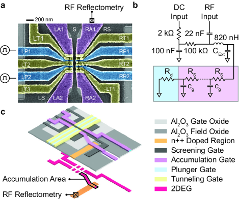
The quantum dot devices in this report are fabricated on an undoped Si/SiGe heterostructure with an 8-nm-thick Si quantum well approximately 50 nm below the surface. Voltages applied to three overlapping layers of aluminum gates are used to confine electrons in up to four quantum dots Angus et al. (2007); Zajac et al. (2015) (Fig 1a).
We optimized a quantum dot device for rf reflectometry through the following design rules. First, the capacitance between the accumulation gate associated with the readout circuit and the 2DEG, , should satisfy F. Second, the total resistance of the path between the doped region associated with the readout circuit and the sensor dot, , should satisfy , where is the resistance per square of the 2DEG. Satisfying this condition likely ensures that for typical accumulation gate voltages and densities in Si/SiGe. Here is the resistance of the sensor dot. We arrived at these empirical design rules by evaluating several prototype devices (Table I). As described below, the final device design has vastly reduced values of and compared to initial devices.
To accommodate these design rules, the region in the reflectometry circuit extends to within 10 m of the sensor dot, which helps to reduce (Fig. 1c). We use a screening gate West et al. (2019), which runs underneath the accumulation gate associated with the reflectometry circuit, RA1, to reduce as much as possible. Additionally, we remove the quantum well everywhere under RA1 except between the region and the dot via a dry etch process to ensure a minimization of . The accumulation gate corresponding to the rf channel has a area consisting of roughly squares between the screening gate and the dot. The device has a 15-nm-thick Al2O3 gate-oxide layer and a 30-nm-thick Al2O3 field-oxide layer. While a thinner gate-oxide layer reduces charge noise Connors et al. (2019), it increases . Although a matching capacitor can improve sensitivity of reflectometry in devices with large Ares et al. (2016), the large , which is distributed with , seemed to prevent success with this approach in our devices. The device optimization described above represents a relatively simple method to implement rf reflectometry, and it should be widely applicable to most accumulation-mode Si quantum dot devices.
| Device | Accumulation Area | Sensitivity | ||
|---|---|---|---|---|
| FET | 9 | - | - | |
| QD 0 | 0 | - | ||
| QD 1 | 83 | 11 | 5 | - |
| QD 2 | 30 | 8 | 25 | |
| QD 3 | 12 | 8 | 27 |
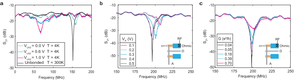
The above mentioned design criteria were evaluated in a prototype two-gate field effect transistor (FET) consisting of an accumulation gate spanning source and drain contacts and a depletion gate used to modulate the channel conductance. The relevant geometries of the FET device were designed to mimic the rf reflectometry circuit in a quantum dot device. To evaluate the rf reflectometry performance, we cooled the prototype device to approximately 4 K and measured using a network analyzer connected to the device via a bias tee and directional coupler. For comparison, Figure 2a shows the rf response of a quantum dot device not optimized for rf reflectometry while 2b and 2c are the results of measurements performed on the FET. Figure 2b shows the response of the reflected signal to the accumulation gate voltage while using the depletion gate to fully suppress the channel conductance. The observed resonance is strongly affected by the gate voltage, demonstrating the capability of using an accumulation gate for in-situ impedance matching. Once the circuit is matched via adjustments to the accumulation gate voltage, the reflected rf signal is sufficiently sensitive to changes in the channel conductance induced by the depletion gate (Fig. 2c). A summary of relevant design parameters and performance metrics for select devices used to prototype the rf reflectometry optimization, including revisions of quantum dot devices, is given in Table I. The design rules and all results in the following sections pertain to device QD 3.
III Charge State Readout
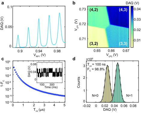
We cool our rf reflectometry optimized device (QD 3 in Table I) in a dilution refrigerator to a base temperature of approximately 50 mK and tune the gate voltages to form a sensor quantum dot under plunger gate RP1. We apply an rf excitation at MHz to the ohmic contact corresponding to RA1, which is part of the impedance-matching circuit. The rf carrier is generated at 10 dBm and sees 36 dB, 20 dB, and 13 dB of attenuation at room temperature, 1.5 K, and 50 mK, respectively. The circuit also consists of an 820-nH surface mount inductor and the stray capacitance of the device, (Fig. 1b). The reflected rf signal is amplified by 38 dB via a Cosmic Microwave Technologies CITLF3 cryogenic amplifier at approximately 4 K and an additional 54 dB via a Narda-MITEQ AU-1565 amplifier at room temperture before it is digitized on an AlazarTech ATS9440 data acquisition card (DAQ) Reilly et al. (2007). During the tune-up process, we adjust the accumulation gate voltage, which affects both and , to optimize the sensitivity of the circuit Angus et al. (2008). We observe a strong modulation in the reflected signal as the plunger gate sweeps across conductance peaks (Fig. 3a).
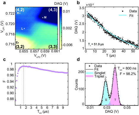
To perform charge sensing, we set the plunger gate voltage to the side of a conductance peak such that the reflected rf signal is sensitive to small changes in the electrochemical potential of the dot. We then tune the gates on the left side of the device to form a double quantum dot, and acquire charge stability diagrams by measuring the reflected rf signal while varying the voltages on plunger gates LP1 and LP2 (Fig. 3b).
We quantify the charge state readout performance by tuning the left-side double dot to the (1,0) occupancy, where the notation refers to the charge configuration with electrons in the dot under gate LP1(LP2). We adjust the tunnel barrier coupling the dot under LP1 to its reservoir such that the tunneling rate is of order 10 Hz. We set the voltage of the plunger gate directly on the (0,0)-(1,0) transition and acquire a time series of the reflected signal, and we resolve individual charge tunneling events Zajac et al. (2016) (Fig. 3c). We fit a histogram of the data (Fig. 3d) to a function where
| (1) |
is a Gaussian with amplitude, mean, and standard deviation , and , respectively. indicates the occupation of the dot, and is the measured voltage.
We define the measurement fidelity associated with occupation as
| (2) |
The integral bounds in Equation 2 are and for , and and for , where is the threshold voltage. is chosen to maximize the charge state readout fidelity
| (3) |
Both and depend on the per-point integration time . In our device, we achieve a charge state readout fidelity of and signal to noise ratio of with an integration time as small as ns (Fig. 3d). By extending the integration time to just ns, we achieve a charge state readout fidelity [Fig. 3c].
IV Singlet-Triplet Readout
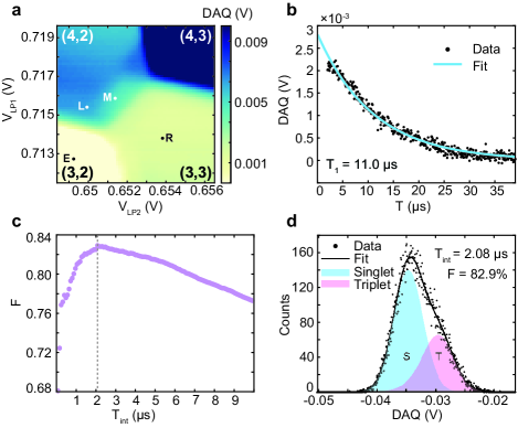
Having demonstrated fast high-fidelity charge sensing, we turn to fast readout of spin states. We observe Pauli spin blockade at the transition in this device. (We did not observe spin blockade at the transition, likely because of a small valley splitting.) We repeatedly apply a three-step pulse sequence that initializes a random spin state in (3,3) prior to pulsing toward the measurement point, at which point the rf excitation is applied to the sensor dot. When the randomly loaded spin state is a singlet, it can tunnel freely from (3,3) to (4,2). If it is a triplet, it remains blockaded in (3,3) until it either undergoes a spin flip or exchanges electrons with the reservoirs. We vary the position of the measurement point, and plot the average signal acquired at each measurement point in Fig. 4a. A trapezoid indicating the spin blockade region is visible in the (4,2) charge configuration near the interdot transition.
To quantify the singlet-triplet readout fidelity, we perform 10,000 single-shot measurements in which we initialize a random spin state before pulsing to the measurement point in the spin blockade region, and an additional 10,000 measurements in which we instead preferentially initialize a singlet state prior to measurement. The two sequences described above pulse the gates between positions E, R, and M in Figure 4a, and positions E, R, L, and M, respectively. At the measurement point, we acquire a time series of the reflected rf signal for s for each single-shot measurement. The average difference between these signals as a function of measurement time from 0-40 s is shown in Fig. 4b. These data follow a characteristic exponential decay with a relaxation time s. In fitting this data, we discard the first 2.5 s of data at the beginning of each measurement to allow for the circuit to ring up. The value of that we measure is lower than typical spin relaxation times in Si based quantum dots Zajac et al. (2016). This fast relaxation is likely related to the rf excitation and strong coupling between the dots and reservoirs in this device.
To compute a measurement fidelity, we use Equations (1)-(3) of Ref. Barthel et al. (2009) to fit a histogram of the data from the first pulse sequence discussed above to the sum of two noise broadened peaks with additional terms to account for relaxation Barthel et al. (2009). We extract the readout fidelity as , where and are the singlet and triplet readout fidelities Barthel et al. (2009). We choose the singlet-triplet threshold voltage to maximize the overall fidelity. Despite the enhanced triplet to singlet relaxation, we achieve a maximum fidelity of in s (Fig. 4d). In this approach, we discard the first 500 ns of data to allow the resonator to ring up. The total measurement time is thus s. In computing the fidelity, we have accounted for spin relaxation during this 500-ns interval.
To improve our readout fidelity, we use a charge latching mechanism Studenikin et al. (2012); Mason et al. (2015); Harvey-Collard et al. (2018). We tune our device such that the tunneling rate between the dot under LP1 and its corresponding reservoir is and the tunneling rate between the dot under LP2 and its corresponding reservoir is . In this tuning, we again apply a three-step pulse sequence that loads a random state prior to pulsing to the measurement point, and vary the measurement point (Fig. 5a). The charge latching mechanism allows singlet states to tunnel across to (4,2), but triplet states instead preferentially tunnel to an excited charge state in (4,3). Generally, this technique results in better sensitivity than conventional spin-blockade readout, because the total electron number differs between these states.
We characterize the readout by performing 10,000 single-shot measurements at position M in Fig. 5a after initializing a random state by pulsing to positions E and then R, as well as after initializing a singlet state by pulsing to positions E, R, and then L. We observe a longer decay time of s [Fig. 5b], which is likely due to the reduced electron exchange rate with the reservoir connected to the double dot via the slow tunnel barrier. We compute the fidelity as before, but we now subtract an additional mapping error Harvey-Collard et al. (2018) . Here, ns is the average tunneling time across the tunnel barrier connecting the dot under LP1 to its reservoir, and ns is the time we discard once the rf excitation is applied to allow the resonator to ring-up and the latching process to take place. is the average probability during the integration time that a triplet will not have tunneled to the state and will be mistakenly identified as a singlet. Figure 5c shows the fidelity as a function of integration time for this method. We achieve a fidelity with an integration time as short as [Fig 5d], and an improved maximum fidelity of in s [Fig 5c].
V Single Spin Readout
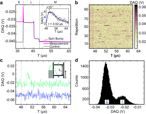
Having demonstrated fast, high-fidelity singlet-triplet state readout, we now discuss fast single-spin readout via spin-selective tunneling Elzerman et al. (2004). Operating the device near the (0,0)-(1,0) transition and with T, we apply a three step pulse sequence Elzerman et al. (2004) to plunger gate LP1 which empties and then loads the corresponding dot with a random spin, and then pulses to the measurement point (Fig. 6a). At the measurement point, which is close to the (1,0)-(0,0) transition, a spin-up electron will preferentially tunnel out. Some time later, a spin-down electron will tunnel back in. This brief change in occupancy results in a measurable change in the charge-sensor signal.
We acquire more than 32,000 single-shot measurements using the pulse sequence described above. For each single-shot measurement, we additionally perform a control measurement using a pulse sequence in which we initialize a spin-down electron instead of an electron with a random spin state. Figure 6a shows plots of the average acquired charge sensor signal across all single-shot traces for both the measurement and control pulse sequences. A “spin bump” from the presence of tunneling events corresponding to spin up electrons is visible at the beginning of the measurement window ranging from s. The signal from the control pulse shows no spin-bump, as expected. The inset of Fig. 6a shows the difference between the average of the control and measurement pulse sequences in the measurement window. We fit these data to a function of the form , where , , and are a fit parameters, and is time from the start of the measurement window. We extract a characteristic tunneling time s. A representative collection of 100 single-shot traces is shown in Figure 6b, and two traces (one spin up and the other spin down) are shown in Fig. 6c.
Figure 6d shows a histogram of the maximum single point value acquired in each single-shot measurement during the measurement window. This histogram shows two distinct peaks corresponding to spin-up and spin-down electrons. The overall acquisition time for each single-shot measurement is only 18 s, orders of magnitude faster than usual spin-selective tunneling measurement times Elzerman et al. (2004). This increase in speed is enabled by the high bandwidth of the reflectometry circuit.
VI Conclusion
We have optimized a Si/SiGe quantum dot device with overlapping gates for rf reflectometry by making only modest geometric changes to our device design. The methods we use are applicable to Si devices with and without overlapping gates, can be implemented with relative ease, preserve the scalability of the gate layout, and, importantly, provide the ability to perform rapid high-fidelity charge and spin state readout. We have demonstrated microsecond-scale readout of single-spin states and sub-microsecond singlet-triplet readout. We expect that further improvements are possible via optimization of the dot-reservoir couplings and the sensor dot position. This work presents a feasible solution to achieving rapid and high-fidelity spin-state readout in Si spin qubits that is largely compatible with existing device designs.
During the completion of this manuscript, we became aware of a related result demonstrating similar techniques for the implementation of rf reflectometry in accumulation mode Si devices Noiri et al. (2020).
We thank Aaron Mitchell Jones for valuable discussions. We thank Lisa F. Edge of HRL Laboratories, LLC. for the epitaxial growth of the SiGe material. Research was sponsored by the Army Research Office and was accomplished under Grant Numbers W911NF-16-1-0260 and W911NF-19-1-0167. The views and conclusions contained in this document are those of the authors and should not be interpreted as representing the official policies, either expressed or implied, of the Army Research Office or the U.S. Government. The U.S. Government is authorized to reproduce and distribute reprints for Government purposes notwithstanding any copyright notation herein. E.J.C. was supported by ARO and LPS through the QuaCGR Fellowship Program.
References
- Veldhorst et al. (2014) M Veldhorst, J C C Hwang, C H Yang, A W Leenstra, Bob de Ronde, J P Dehollain, J T Muhonen, F E Hudson, Kohei M Itoh, A Morello, et al., “An addressable quantum dot qubit with fault-tolerant control-fidelity,” Nature Nanotechnology 9, 981 (2014).
- Tyryshkin et al. (2012) Alexei M Tyryshkin, Shinichi Tojo, John J L Morton, Helge Riemann, Nikolai V Abrosimov, Peter Becker, Hans-Joachim Pohl, Thomas Schenkel, Michael L W Thewalt, Kohei M Itoh, et al., “Electron spin coherence exceeding seconds in high-purity silicon,” Nature Materials 11, 143 (2012).
- Morello et al. (2010) Andrea Morello, Jarryd J Pla, Floris A Zwanenburg, Kok W Chan, Kuan Y Tan, Hans Huebl, Mikko Möttönen, Christopher D Nugroho, Changyi Yang, Jessica A van Donkelaar, et al., “Single-shot readout of an electron spin in silicon,” Nature 467, 687 (2010).
- Yoneda et al. (2018) Jun Yoneda, Kenta Takeda, Tomohiro Otsuka, Takashi Nakajima, Matthieu R Delbecq, Giles Allison, Takumu Honda, Tetsuo Kodera, Shunri Oda, Yusuke Hoshi, et al., “A quantum-dot spin qubit with coherence limited by charge noise and fidelity higher than 99.9%,” Nature Nanotechnology 13, 102 (2018).
- Eng et al. (2015) Kevin Eng, Thaddeus D Ladd, Aaron Smith, Matthew G Borselli, Andrey A Kiselev, Bryan H Fong, Kevin S Holabird, Thomas M Hazard, Biqin Huang, Peter W Deelman, et al., “Isotopically enhanced triple-quantum-dot qubit,” Science Advances 1, e1500214 (2015).
- Maune et al. (2012) Brett M Maune, Matthew G Borselli, Biqin Huang, Thaddeus D Ladd, Peter W Deelman, Kevin S Holabird, Andrey A Kiselev, Ivan Alvarado-Rodriguez, Richard S Ross, Adele E Schmitz, et al., “Coherent singlet-triplet oscillations in a silicon-based double quantum dot,” Nature 481, 344 (2012).
- Watson et al. (2018) T F Watson, S G J Philips, Erika Kawakami, D R Ward, Pasquale Scarlino, Menno Veldhorst, D E Savage, M G Lagally, Mark Friesen, S N Coppersmith, et al., “A programmable two-qubit quantum processor in silicon,” Nature 555, 633 (2018).
- Veldhorst et al. (2015) Menno Veldhorst, C H Yang, J C C Hwang, W Huang, J P Dehollain, J T Muhonen, S Simmons, A Laucht, F E Hudson, Kohei M Itoh, et al., “A two-qubit logic gate in silicon,” Nature 526, 410 (2015).
- Xue et al. (2019) X Xue, T F Watson, J Helsen, Daniel R Ward, Donald E Savage, Max G Lagally, Susan N Coppersmith, M A Eriksson, S Wehner, and L M K Vandersypen, “Benchmarking gate fidelities in a Si/SiGe two-qubit device,” Physical Review X 9, 021011 (2019).
- Vandersypen and Eriksson (2019) Lieven M K Vandersypen and Mark A Eriksson, “Quantum computing with semiconductor spins,” Physics Today 72, 38–45 (2019).
- Zhang et al. (2018) Xin Zhang, Hai-Ou Li, Gang Cao, Ming Xiao, Guang-Can Guo, and Guo-Ping Guo, “Semiconductor quantum computation,” National Science Review 6, 32–54 (2018).
- Fowler et al. (2012) Austin G Fowler, Matteo Mariantoni, John M Martinis, and Andrew N Cleland, “Surface codes: Towards practical large-scale quantum computation,” Physical Review A 86, 032324 (2012).
- Zajac et al. (2016) D M Zajac, T M Hazard, Xiao Mi, E Nielsen, and J R Petta, “Scalable gate architecture for a one-dimensional array of semiconductor spin qubits,” Physical Review Applied 6, 054013 (2016).
- Mortemousque et al. (2018) Pierre-Andre Mortemousque, Emmanuel Chanrion, Baptiste Jadot, Hanno Flentje, Arne Ludwig, Andreas D. Wieck, Matias Urdampilleta, Christopher Bauerle, and Tristan Meunier, “Coherent control of individual electron spins in a two dimensional array of quantum dots,” (2018), arXiv:1808.06180 .
- Mukhopadhyay et al. (2018) Uditendu Mukhopadhyay, Juan Pablo Dehollain, Christian Reichl, Werner Wegscheider, and Lieven M. K. Vandersypen, “A 2 x 2 quantum dot array with controllable inter-dot tunnel couplings,” Applied Physics Letters 112, 183505 (2018).
- Simmons et al. (2011) C. B. Simmons, J. R. Prance, B. J. Van Bael, Teck Seng Koh, Zhan Shi, D. E. Savage, M. G. Lagally, R. Joynt, Mark Friesen, S. N. Coppersmith, and M. A. Eriksson, “Tunable spin loading and of a silicon spin qubit measured by single-shot readout,” Phys. Rev. Lett. 106, 156804 (2011).
- Thalakulam et al. (2011) Madhu Thalakulam, C. B. Simmons, B. J. Van Bael, B. M. Rosemeyer, D. E. Savage, M. G. Lagally, Mark Friesen, S. N. Coppersmith, and M. A. Eriksson, “Single-shot measurement and tunnel-rate spectroscopy of a Si/SiGe few-electron quantum dot,” Phys. Rev. B 84, 045307 (2011).
- Field et al. (1993) M. Field, C. G. Smith, M. Pepper, D. A. Ritchie, J. E. F. Frost, G. A. C. Jones, and D. G. Hasko, “Measurements of coulomb blockade with a noninvasive voltage probe,” Phys. Rev. Lett. 70, 1311–1314 (1993).
- Elzerman et al. (2003) J. M. Elzerman, R. Hanson, J. S. Greidanus, L. H. Willems van Beveren, S. De Franceschi, L. M. K. Vandersypen, S. Tarucha, and L. P. Kouwenhoven, “Few-electron quantum dot circuit with integrated charge read out,” Phys. Rev. B 67, 161308 (2003).
- Pla et al. (2012) Jarryd J Pla, Kuan Y Tan, Juan P Dehollain, Wee H Lim, John J L Morton, David N Jamieson, Andrew S Dzurak, and Andrea Morello, “A single-atom electron spin qubit in silicon,” Nature 489, 541 (2012).
- Broome et al. (2017) M. A. Broome, T. F. Watson, D Keith, S. K. Gorman, M. G. House, J. G. Keizer, S. J. Hile, W Baker, and M. Y. Simmons, “High-fidelity single-shot singlet-triplet readout of precision-placed donors in silicon,” Physical review letters 119, 046802 (2017).
- Colless et al. (2013) J. I. Colless, A. C. Mahoney, J. M. Hornibrook, A. C. Doherty, H Lu, A. C. Gossard, and D. J. Reilly, “Dispersive readout of a few-electron double quantum dot with fast rf gate sensors,” Physical review letters 110, 046805 (2013).
- Pakkiam et al. (2018) P Pakkiam, A. V. Timofeev, M. G. House, M. R. Hogg, T Kobayashi, M Koch, S Rogge, and Michelle Y Simmons, “Single-shot single-gate rf spin readout in silicon,” Physical Review X 8, 041032 (2018).
- Zheng et al. (2019) Guoji Zheng, Nodar Samkharadze, Marc L Noordam, Nima Kalhor, Delphine Brousse, Amir Sammak, Giordano Scappucci, and Lieven M K Vandersypen, “Rapid gate-based spin read-out in silicon using an on-chip resonator,” Nature nanotechnology 14, 742–746 (2019).
- Urdampilleta et al. (2019) Matias Urdampilleta, David J. Niegemann, Emmanuel Chanrion, Baptiste Jadot, Cameron Spence, Pierre-André Mortemousque, Christopher Bäuerle, Louis Hutin, Benoit Bertrand, Sylvain Barraud, Romain Maurand, Marc Sanquer, Xavier Jehl, Silvano De Franceschi, Maud Vinet, and Tristan Meunier, “Gate-based high fidelity spin readout in a cmos device,” Nature Nanotechnology 14, 737–741 (2019).
- West et al. (2019) Anderson West, Bas Hensen, Alexis Jouan, Tuomo Tanttu, Chih-Hwan Yang, Alessandro Rossi, M Fernando Gonzalez-Zalba, Fay Hudson, Andrea Morello, David J Reilly, et al., “Gate-based single-shot readout of spins in silicon,” Nature nanotechnology 14, 437 (2019).
- Volk et al. (2019a) C. Volk, A. M. J. Zwerver, U. Mukhopadhyay, P. T. Eendebak, C. J. van Diepen, J. P. Dehollain, T. Hensgens, T. Fujita, C. Reichl, W. Wegscheider, and L. M. K. Vandersypen, “Loading a quantum-dot based ”qubyte” register,” npj Quantum Information 5, 29 (2019a).
- Kandel et al. (2019) Yadav P. Kandel, Haifeng Qiao, Saeed Fallahi, Geoffrey C. Gardner, Michael J. Manfra, and John M. Nichol, “Coherent spin-state transfer via heisenberg exchange,” Nature 573, 553–557 (2019).
- Qiao et al. (2019) Haifeng Qiao, Yadav P. Kandel, Sreenath K. Manikandan, Andrew N. Jordan, Saeed Fallahi, Geoffrey C. Gardner, Michael J. Manfra, and John M. Nichol, “Conditional teleportation of quantum-dot spin states,” (2019), arXiv:1908.08306 .
- Vink et al. (2007) I T Vink, T Nooitgedagt, R N Schouten, L M K Vandersypen, and Werner Wegscheider, “Cryogenic amplifier for fast real-time detection of single-electron tunneling,” Applied Physics Letters 91, 123512 (2007).
- Jones et al. (2019) A. M. Jones, E. J. Pritchett, E. H. Chen, T. E. Keating, R. W. Andrews, J. Z. Blumoff, L. A. De Lorenzo, K. Eng, S. D. Ha, A. A. Kiselev, S. M. Meenehan, S. T. Merkel, J. A. Wright, L. F. Edge, R. S. Ross, M. T. Rakher, M. G. Borselli, and A. Hunter, “Spin-blockade spectroscopy of /- quantum dots,” Phys. Rev. Applied 12, 014026 (2019).
- Schoelkopf et al. (1998) R. J. Schoelkopf, P. Wahlgren, A. A. Kozhevnikov, P. Delsing, and D. E. Prober, “The radio-frequency single-electron transistor (rf-set): A fast and ultrasensitive electrometer,” Science 280, 1238–1242 (1998).
- Reilly et al. (2007) D J Reilly, C M Marcus, M P Hanson, and A C Gossard, “Fast single-charge sensing with a rf quantum point contact,” Applied Physics Letters 91, 162101 (2007).
- Taskinen et al. (2008) L J Taskinen, R P Starrett, T P Martin, A P Micolich, A R Hamilton, M Y Simmons, D A Ritchie, and M Pepper, “Radio-frequency reflectometry on large gated two-dimensional systems,” Review of Scientific Instruments 79, 123901 (2008).
- Barthel et al. (2009) Christian Barthel, D. J. Reilly, Charles Masamed Marcus, M. P. Hanson, and A. C. Gossard, “Rapid single-shot measurement of a singlet-triplet qubit,” Physical Review Letters 103, 160503 (2009).
- Barthel et al. (2010) Christian Barthel, Morten Kjærgaard, J Medford, M Stopa, Charles Masamed Marcus, M. P. Hanson, and Arthur C Gossard, “Fast sensing of double-dot charge arrangement and spin state with a radio-frequency sensor quantum dot,” Physical Review B 81, 161308 (2010).
- Higginbotham et al. (2014) Andrew Patrick Higginbotham, Ferdinand Kuemmeth, Micah P Hanson, Arthur C Gossard, and Charles M Marcus, “Coherent operations and screening in multielectron spin qubits,” Physical Review Letters 112, 026801 (2014).
- Villis et al. (2014) B. J. Villis, A. O. Orlov, S. Barraud, M. Vinet, M. Sanquer, P. Fay, G. Snider, and X. Jehl, “Direct detection of a transport-blocking trap in a nanoscaled silicon single-electron transistor by radio-frequency reflectometry,” Applied Physics Letters 104, 233503 (2014).
- Hile et al. (2015) Samuel J Hile, Matthew G House, Eldad Peretz, Jan Verduijn, Daniel Widmann, Takashi Kobayashi, Sven Rogge, and Michelle Y Simmons, “Radio frequency reflectometry and charge sensing of a precision placed donor in silicon,” Applied Physics Letters 107, 093504 (2015).
- Angus et al. (2008) S. J. Angus, A. J. Ferguson, A. S. Dzurak, and R. G. Clark, “A silicon radio-frequency single electron transistor,” Applied Physics Letters 92, 112103 (2008).
- Ares et al. (2016) N. Ares, F. J. Schupp, A. Mavalankar, G. Rogers, J. Griffiths, G. A. C. Jones, I. Farrer, D. A. Ritchie, C. G. Smith, A. Cottet, G. A. D. Briggs, and E. A. Laird, “Sensitive Radio-Frequency Measurements of a Quantum Dot by Tuning to Perfect Impedance Matching,” Physical Review Applied 5, 034011 (2016).
- Wang et al. (2013) K Wang, C Payette, Y Dovzhenko, P W Deelman, and Jason R Petta, “Charge relaxation in a single-electron si/sige double quantum dot,” Physical review letters 111, 046801 (2013).
- Volk et al. (2019b) Christian Volk, Anasua Chatterjee, Fabio Ansaloni, Charles M. Marcus, and Ferdinand Kuemmeth, “Fast charge sensing of Si/SiGe quantum dots via a high-frequency accumulation gate,” Nano Letters 19, 5628–5633 (2019b).
- Angus et al. (2007) Susan J. Angus, Andrew J. Ferguson, Andrew S. Dzurak, and Robert G. Clark, “Gate-defined quantum dots in intrinsic silicon,” Nano Letters 7, 2051–2055 (2007).
- Zajac et al. (2015) D M Zajac, T M Hazard, X Mi, K Wang, and J R Petta, “A reconfigurable gate architecture for Si/SiGe quantum dots,” Applied Physics Letters 106, 223507 (2015).
- Connors et al. (2019) Elliot J. Connors, JJ Nelson, Haifeng Qiao, Lisa F. Edge, and John M. Nichol, “Low-frequency charge noise in Si/SiGe quantum dots,” Phys. Rev. B 100, 165305 (2019).
- Studenikin et al. (2012) S A Studenikin, J Thorgrimson, G C Aers, A Kam, P Zawadzki, Z R Wasilewski, A Bogan, and A S Sachrajda, “Enhanced charge detection of spin qubit readout via an intermediate state,” Applied Physics Letters 101, 233101 (2012).
- Mason et al. (2015) J. D. Mason, S. A. Studenikin, A. Kam, Z. R. Wasilewski, A. S. Sachrajda, and J. B. Kycia, “Role of metastable charge states in a quantum-dot spin-qubit readout,” Phys. Rev. B 92, 125434 (2015).
- Harvey-Collard et al. (2018) Patrick Harvey-Collard, Benjamin D’Anjou, Martin Rudolph, N Tobias Jacobson, Jason Dominguez, Gregory A Ten Eyck, Joel R Wendt, Tammy Pluym, Michael P Lilly, William A Coish, et al., “High-fidelity single-shot readout for a spin qubit via an enhanced latching mechanism,” Physical Review X 8, 021046 (2018).
- Elzerman et al. (2004) J. M. Elzerman, R Hanson, L. H. Willems Van Beveren, B Witkamp, L. M. K. Vandersypen, and Leo P Kouwenhoven, “Single-shot read-out of an individual electron spin in a quantum dot,” nature 430, 431 (2004).
- Noiri et al. (2020) Akito Noiri, Kenta Takeda, Jun Yoneda, Takashi Nakajima, Tetsuo Kodera, and Seigo Tarucha, “Radio-frequency detected fast charge sensing in undoped silicon quantum dots,” Nano Letters (2020), 10.1021/acs.nanolett.9b03847, pMID: 31944116.