Resistive contribution in electrical switching experiments with antiferromagnets
Abstract
Recent research demonstrated the electrical switching of antiferromagnets via intrinsic spin-orbit torque or the spin Hall effect of an adjacent heavy metal layer. The electrical readout is typically realized by measuring the transverse anisotropic magnetoresistance at planar cross- or star-shaped devices with four or eight arms, respectively. Depending on the material, the current density necessary to switch the magnetic state can be large, often close to the destruction threshold of the device. We demonstrate that the resulting electrical stress changes the film resistivity locally and thereby breaks the fourfold rotational symmetry of the conductor. This symmetry breaking due to film inhomogeneity produces signals, that resemble the anisotropic magnetoresistance and is experimentally seen as a “saw-tooth”-shaped transverse resistivity. This artifact can persist over many repeats of the switching experiment and is not easily separable from the magnetic contribution. We discuss the origin of the artifact, elucidate the role of the film crystallinity, and propose approaches how to separate the resistive contribution from the magnetic contribution.
I Introduction
The possibility to switch the magnetic order of antiferromagnets (AFM) with electric currents has been predicted about five years ago Železný et al. (2014). It was theoretically shown that materials of certain symmetry can exhibit staggered nonequilibrium spin polarization. If these coincide with the crystallographic positions of the staggered magnetic moments, a net torque on the antiferromagnetic order arises, which enables its current-driven reorientation. While the effect was predicted for Mn2Au, its first realization was demonstrated with CuMnAs Wadley et al. (2016). Later, the Néel-order switching was also shown for Mn2Au films Meinert et al. (2018); Bodnar et al. (2018); Zhou et al. (2018). A greater variety of AFM can be switched using heterostructures that utilize the spin Hall effect (SHE) in an adjacent heavy metal (HM) like Pt to exert an antidamping torque on the Néel-order Chen et al. (2018); Moriyama et al. (2018); Gray et al. (2018); Baldrati et al. (2018); Zhou et al. (2019); Dunz et al. (2019). The reorientation can be realized with cross-shaped planar devices, where electrical pulses driven through the orthogonal lines allow for a reproducible switching of the Néel-order by 90∘. In AFM/HM heterostructures there are two possible readout mechanisms with identical symmetry. The spin-polarized current in the HM is partially absorbed by the AFM, which depends on the relative orientation of the polarization and the magnetic moments in the AFM. This gives rise to the spin Hall magnetoresistance (SMR). The second mechanism is the anisotropic magnetoresistance (AMR). In both cases, typically for the current flowing parallel or perpendicular to the magnetic moments is found. In single layer switching experiments, only the AMR is available for electrical readout. To observe the rather small resistivity change associated with the AMR or SMR, it is favorable to measure in transverse geometry. For a sense current density , the associated transverse electric field is given by , where is the angle between sense current density and magnetic moments. The experiment is performed by recording the transverse voltage with a fixed sense current in a device as sketched in Fig. 1 (a). In this type of experiments, Cheng et al. identified a “saw-tooth”-shaped contribution in measurements arising from the Pt layer for large current density Cheng et al. (2019), which is of nonmagnetic origin. It was found to be larger than the magnetic contribution to the transverse electrical response in some cases.
In the present manuscript, we investigate the origin of this nonmagnetic contribution to the electrical response of the star-shaped structures. We chose paramagnetic Nb films as a model system, because here no magnetic contribution is present. Two different types of films are compared, grown either at room temperature (polycrystalline) or at high temperature (epitaxial). We analyze the response to current pulses and inspect the star-shaped devices in operando by x-ray microdiffraction (µXRD) and scanning electron microscopy (SEM). Our findings are consistent with the results presented in Ref. Cheng et al. (2019), where a change of with the planar Hall effect symmetry is observed in Pt films. We interpret this observation as a local variation of the film resistivity which gives rise to a change with alternating sign for the different pulsing directions. Calculations using a finite-element-method (FEM) show that the effect size is in quantitative agreement with this explanation. Furthermore we see that the sign of can change within one experiment highlighting that at least two processes of nonmagnetic origin can be present in such experiments, related to locally decreasing or increasing resistivities.
II Sample characteristics and experimental setup
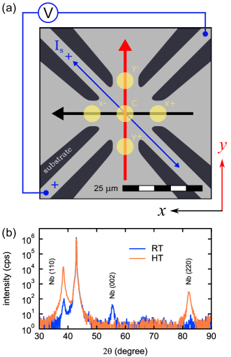
Samples of MgO (001) / Nb 25 nm / Si 2 nm were grown by magnetron sputtering at room temperature (RT) and at (high-temperature, HT). The Si capping prevents oxidation of the films. The film quality is characterized by x-ray diffraction (XRD). The RT sample shows no preferred growth direction, whereas the HT sample grows in (110) direction, see Fig. 1 (b). The resistivities are and , determined by four-point measurements on the films. Finally, the films are patterned to star-shaped devices as depicted in Fig. 1 (a) by photolithography and wire-bonded into IC packages. On each sample, half of the devices have their pulse lines () aligned parallel to the [100] ([010]) direction of the substrate, the other half of the devices are rotated by .
The experimental procedure for the electrical experiments is similar to our experiment on Néel-order switching in CuMnAs, see Ref. Matalla-Wagner et al. (2019). We apply bursts of current pulses to our structure in one of two orthogonal directions and (cf. Fig. 1 (a)). The pulses have a length of and a duty cycle of . The number of pulses per burst is not constant in this work but typically a burst consists of around 100 pulses. After each burst, we measure with a lock-in amplifier. We also observe the evolution of after the burst sequence during a relaxation-phase. The pulse-line resistances and are measured prior to the burst sequence with a Keithley multimeter to set the voltage output of the arbitrary waveform generator accordingly. The experiments are additionally performed with simultaneous µXRD measurements or SEM imaging. The µXRD investigation was conducted at beamline of the Advanced Light Source (ALS), Berkeley, California, USA Kunz et al. (2009). We measure diffraction patterns with a PILATUS 1M detector and an integration time of for the beam located on the constrictions of each pulseline and in the center of the device, as highlighted by the yellow areas in Fig. 1 (a). The spot size is approximately 5 µm and the energy is tuned to match the diffraction conditions.
III Results
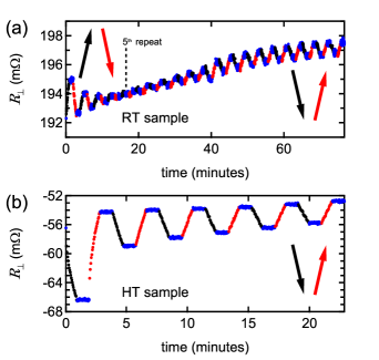
A pulsing experiment performed with Nb thin films is presented in Fig. 2. Panel (a) shows the change of for the RT sample with a current density of applied alternating to the and pulseline. The respective relaxation is observed for . We observe a significant change of during pulsing, whereas remains stable during the relaxation. Initially, pulsing along increases while pulsing along decreases . The amplitude of this „saw-tooth“ signal decreases with each repeat and vanishes around the fifth repeat. The following repeats show an inverted sign of the response with virtually constant amplitude. An overall trend towards higher values of is present which is most likely related to asymmetries arising from imperfect lithography. The polarity of the pulse current has no impact on the signal (not shown). Panel (b) of Fig. 2 shows an equivalent measurement for the HT sample. However, a higher current density of had to be applied to observe a transverse electrical response of similar magnitude. From a current density variation we find, that the HT sample only shows one sign of transverse resistance change. The degradation of the transverse resistance amplitude slows down for successive repeats. We observe no qualitative difference in behavior between devices with or .
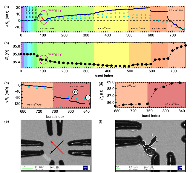
In the following, we investigate a fresh device on the RT sample and take SEM images after each pulsing experiment with the device grounded while taking the image. Here, we primarily pulse along and use pulses in direction only to demonstrate that the sign of depends on the pulsing direction as before. The response of the system and the values of taken intermittently are plotted in Fig. 3 (a) and (b), respectively. For we neither see a transverse response nor a change of . Starting with we observe a response with and a decrease of . Further increasing , enhances the transverse response and the resistance change alike. Pulsing in direction changes the sign of and has no impact on . For successive bursts in the same direction, and seem to saturate until is increased again. At , we observe a crossover between reducing and increasing , where the change of the transverse response also changes sign. This change in sign becomes more apparent for even higher until a response similar to Fig. 2 (b) is obtained for . The effect size greatly enhances for as seen in Fig. 3 (c) and (d). For this current density, we observe that the transverse response intermittently has a positive sign, while the overall trend is negative. increases with each successive experiment until the device breaks. We were not able to resolve any change of the device in SEM images for . However, from the first sequence at until the destruction of the device we see clear changes arising at the lower left constriction of the structure. An exemplary image taken after the second repeat with highest is shown in Fig. 3 (e). With the first burst of the fifth repeat the device breaks (cf. Fig. 3 (f)) with droplets of material moving in electron flow direction.
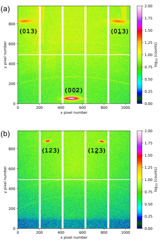
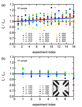
We identified a correlation between and where the physical origin of this resistance change needs to be clarified. In the following, we attempt to investigate whether local annealing due to the Joule heating may contribute to the observed behavior. To this end, we perform µXRD observations of selected x-ray diffraction peaks while performing pulsing experiments. Exemplarily, we show 2D diffractograms in Fig. 4. The positions of the x-ray focus are shown in Fig. 1 (a). During the experiment, we do not observe any changes of the peak positions. To determine the crystallinity of the samples, we define regions of interest (ROI) around the peak positions and calculate the integrated intensity , with being the counts of each pixel and being the experiment index. The x-ray intensity of the beamline varies slightly over time, so we normalize to the background signal which is calculated from an ROI that contains only diffuse scattering and fluorescence signals. In Fig. 5, we plot the normalized peak intensity divided by its initial value against the experiment index, which is essentially a number raised with each pulsing-relaxation sequence containing no information about or the pulsing direction. (a) and (b) show the data measured at the RT and HT sample, respectively. We repeat pulsing experiments either until the sign of the response inverts or the device breaks. Unfortunately, the signal-to-noise ratio is rather unsatisfying despite the integration times of up to per image. Instead of looking at the individual positions, we collect all datasets and apply a linear regression with fixed to extract the trend of peak intensity under repeated electrical pulsing. In Fig. 5, these regressions are visualized by the blue lines. We find a significantly positive slope of for the device on the RT sample. The HT sample was destroyed during the experiment with index 7 where pulses were applied in direction. It can be seen in Fig. 5 (c) that the peak intensity measured at the position after destruction is significantly reduced compared to the other positions. An optical micrograph verifies that indeed the constriction is the one which broke during the experiment. Linear regression with gives , i.e. no significant change in peak intensity is observed. Thus we conclude that the crystallinity of the RT sample is enhanced due to the electrical pulsing. For the HT sample, no enhancement of the crystallinity is observed.
IV Discussion
When a sense current is passed through a material, the appearance of a transverse electric field is generally due to a breaking of the mirror symmetry of the resistivity about the current direction. For the AMR and SMR, this is due to and the current being neither parallel nor perpendicular to the magnetic moments. As we have shown in this study, one can observe a transverse voltage change induced by electrical pulses that largely resembles the electrical switching of the Néel-order in antiferromagnets in devices that are nonmagnetic. Although the amplitude of this nonmagnetic response eventually reduces with successive pulsing, the decay can be marginal and looks like a practically constant amplitude over dozens of repeats.
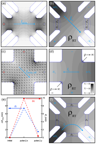
We interpret our experimental findings on Nb films as a symmetry breaking on the (macroscopic) device level rather than on the microscopic level. Due to the Joule heating associated with the large current densities, a local variation of the film resistivity is created. This resistivity change is located in the constrictions of the device where is large compared to the rest of the device. In the following, we attempt to understand the experimental evidence presented before by a finite-element model. Fig. 6 (a) shows the locally resolved current density in our eight-arm devices during a pulse. Additionally, we consider another pulse-current distribution in cross-shaped devices, see Fig. 6 (c), which we discuss later (cf. Ref. Olejník et al. (2017); Meinert et al. (2018)).
The large current density in the constrictions of the device was shown to locally change the film crystallinity and to reduce the resistivity as a consequence. For the simplicity of the model, we consider local changes of the resistivity in rectangular areas within the constrictions as depicted in Fig. 6 (b). In our example, the dimensions of the pulse line constrictions are about and each constriction accounts for of the total pulse line resistance . Assuming that only changes within the constrictions, a change can be translated into a resistivity change within the constriction
| (1) |
with being the pulse line resistance before pulsing. From the resistance variation of the pulse line in Fig. 3 (b) we calculate a maximum of about (around burst index 495). Here, we measure . To check whether can account for , we perform FEM simulations using the software FEMM v4.2 Baltzis (2008); Meeker . The resistivity of the film is set to and the resistivity in the constrictions is (cf. Fig. 6 (b)). We then apply and find that a transverse voltage arises due to the symmetry break about the current direction. The simulated transverse resistance is . critically depends on the exact choice of the shape of the area with , e.g. if we make the area slightly convex (see dotted lines in Fig. 6 (b)), the result increases to . In Fig. 3 (a) we show full calculations with the model using rectangular constrictions, where the local resistivity variation is calculated on the basis of the change in pulse line resistance. We find that the observed transverse resistance is qualitatively well reproduced by the model, although quantitative descrepancies remain, which are probably due to the simplicity of the model. Thus, our conclusion is that the local change in the constrictions of our device contributes largely to the transverse voltage signals. In addition, the sign of the transverse voltage is the same in the FEM calculation and in the experimental lower-current density regime of the RT sample. This implies that the sign change of the transverse resistance in the experiment with the RT sample (cf. Fig. 2 (a)) requires a local increase of the resistivity. This is consistent with Fig. 3 (a) and (b), where the increase of pulse line resistance correlates with a sign reversal in the transverse voltage change. The “saw-tooth”-like electrical response of Fig. 2 (a) and (b) is explained by considering that for pulsing along one direction the mirror symmetry about is gradually broken with every pulse, whereas pulsing along the orthogonal channel restores the mirror symmetry by also reducing/increasing the resistivity in the constrictions. We simulated this situation with the FEM model and show the result in Fig. 6 (e) (right axis). After restoring the mirror symmetry by reducing the local resistivities along both and pulse lines, the transverse voltage drops back to zero within numerical accuracy.
Now we come back to the cross-shaped devices that were used in several previous studies Meinert et al. (2018); Olejník et al. (2017); Baldrati et al. (2018); Moriyama et al. (2018). In this configuration, the pulse voltage is applied to pairs of contacts as depicted in Fig. 6 (c). Here, the maximum current density is found in the corners of the structure. The readout is done with a simple Hall configuration, see Fig. 6 (d). As we lack detailed measurements to compare with, we just show the basic principle of how a transverse voltage arises in this type of device. With respect to the Hall configuration, the mirror symmetry is again broken by the local resistivity change in the corners and restored by pulsing in the orthogonal direction. In the simulation, we consider for simplicity in a small rounded area close to the corners (Fig. 6 (d)). Clearly, this gives rise to a transverse voltage, which can be seen by the distorted equipotential lines. Quantifying the local resistivity changes in this type of device is probably more difficult than in the star-shaped devices. It does therefore seem advisable to preferably make use of star-shaped devices in order to quantify the pulse line resistances for estimating the associated transverse voltage with FEM simulations.
Finally, in some cases a readout configuration as depicted in Fig. 6 (f) is used, which we call “pseudo-longitudinal”. Following previous symmetry-derived arguments, one would not expect an influence of the local resistivity changes. However, our FEM simulation shows that even in this case a change of the pseudo-longitudinal voltage picked up between the top-left and top-right contacts is visible when the constrictions along the and directions change resistivity, cf. Fig. 3 (e). Here, the reason is that the current-density distribution moves along the -direction, such that more current leaks into the film area between the pickup lines. Due to symmetry, this is not fully reversible by orthogonal pulsing and should lead to a “saw-tooth” signal with a prominent drift given by the inverse sign of the local resistivity change. This drift is readily visible in our simulation in Fig. 6 (e). We also note that signal drifts may be ubiquitous as soon as the breaking and restoration of the device symmetry are not perfect, independent of the actual device shape.
V Conclusion
We can conclude that we see two different counteracting mechanisms: on the one hand, the resistivity reduction by crystallization. On the other hand, there is a mechanism that increases the resistivity and destroys the sample eventually. The annealing-like contribution should not be present in the HT sample which is already of good crystallinity. Consistently, we see only one sign of the transverse voltage change in the HT sample, which corresponds to a local increase of the resistivity according to the FEM simulation. The latter is supposedly related to electromigration, which transports material away from the constrictions, thereby creating voids in the material and increasing the local resistivity. The final destruction of the device goes along with a melting of the film and droplets of the material moving in electron flow direction (cf. Fig. 3 (f)). Hence, electromigration is probably the essential mechanism underlying the apparent resistivity increase and eventual breakdown of the device. We note that both the annealing-like component as well as the electromigration-like component are thermally activated and depend on individual energy barriers and the temperature via a Boltzmann factor Jackson (2004). In particular, according to Black’s equation Black (1969)
| (2) |
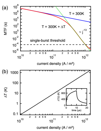
the mean-time-to-failure (MTF) is a strong function of current density and temperature, where the film temperature itself depends strongly on the current density. Here, is the Boltzmann constant and is a scaling factor. Due to the high necessary to switch an AFM, the film temperature may rise by several hundred Kelvin during the pulses You et al. (2006); Meinert et al. (2018); Bodnar et al. (2018). Thus, experiments performed close to the destruction threshold of the devices are particularly prone to the electromigration-like component of the electrical response and results should be taken with care. In Fig. 7, we evaluate Black’s equation within two models, one calculated at fixed , and one calculated at an elevated temperature , where is calculated as a pulse-averaged temperature with You’s formula You et al. (2006) for a pulse width of 10 µs and typical parameters of the MgO substrate (see Ref. Meinert et al. (2018) for details). The parameters for Black’s equation are chosen as and . While is a typical value for grain-boundary self-diffusion Black (1969), is chosen to roughly match the experimental destruction threshold of the device. It can be seen in Fig. 7 (a), that the Joule heating is largely responsible for the short MTF for . Fig. 7 (b) demonstrates that for , the pulse-averaged film temperature is elevated by more than 700 K and may reach even higher temperatures in the final stage of device breakdown, when the constriction becomes even more narrow due to the formation of cracks in the hot-spots. This is consistent with the observed droplets in the destroyed device, see Fig. 3 (f). In the high-current density regime, Black’s equation is often rewritten as to effectively take the Joule heating into account, where . Our numerical estimates suggest that in this specific example, i.e. the MTF shows a very rapid decay with increasing . Because of the similarities in the underlying thermal activation physics, we expect that similar dependencies on measurement temperature and current density may occur due to annealing/electromigration and Néel-order switching. Consequently, it is a difficult task to disentangle the various contributions by electrical experiments alone.
Using a chemically stable capping layer may reduce the surface contribution to the electromigration. However, the volume-contributions of the electromigration can not be reduced by cap layer engineering. As electromigration is a directed transport along the direction of electron flow, one may use single-cycle AC current pulses instead of DC pulses, similar to a previous experiment with CuMnAs Olejník et al. (2018). If the current-pulses are short enough, this should greatly reduce the directed transport, thereby increasing the device lifetime by orders of magnitude Liew et al. (1989). As consequence, the resistivity-enhancing component of the transverse electrical response should be substantially reduced. However, the purely thermal, annealing-like contribution would still be present. This contribution should be relatively easy to remove by pulsed-current annealing the device with a larger current density before systematic investigations of the Néel-order switching are performed. In all cases, it is mandatory to carefully monitor the pulse line resistances and the repeatability of an electrical Néel-order switching experiment to avoid possible confusion of the true planar Hall signal due to switching and the resistive contributions.
As a final remark, we note that we performed similar experiments with films of Ti, V, Mo, and Ta with various degrees of crystal quality, which support our conclusions.
VI Summary
In summary, we investigated the resistive response of star-shaped devices often used in switching experiments with antiferromagnets. We used Nb thin films of different crystallinity and observed different responses in films with either polycrystalline or epitaxial growth. We reason that a change of the resistivity in the constrictions of the devices leads to a transverse voltage in planar Hall effect measurement geometry. From the pulse line resistance changes, we estimate the magnitude of resistivity change in the constrictions and perform FEM simulations that are in semi-quantitative agreement with the experimental data. The decrease and increase of the local resistivity is due to a crystallization and destruction of the sample, respectively. In operando SEM imaging and µXRD measurements support our interpretation. The crystallization or annealing effect is not visible in SEM images, whereas µXRD provides evidence for the local crystallization in polycrystalline films. The sample destruction becomes significant in the transverse and pulse line resistance way before we were able to see any damage in SEM images. This effect resembles the planar Hall effect and is of nonmagnetic origin. Throughout this study, it was found to be irreversible and relaxation was not observed.
For future electrical switching experiments it is thus advisable to regularly measure the pulse line resistances and to check the reproducibility of the switching in, e.g., current density sweeps. As the destructive contribution can be practically constant over a vast number of repeats, the reproducibility of the experiment alone without varying parameters and resistance monitoring does not yield sufficient evidence to exclude the discussed nonmagnetic contributions.
Acknowledgments
This research used beamline 12.3.2 of the Advanced Light Source, which is a DOE Office of Science User Facility under contract no. DE-AC02-05CH11231. We further thank Christan Mehlhaff for conducting preliminary experiments.
References
- Železný et al. (2014) J. Železný, H. Gao, K. Výborný, J. Zemen, J. Mašek, A. Manchon, J. Wunderlich, J. Sinova, and T. Jungwirth, Relativistic Néel-Order Fields Induced by Electrical Current in Antiferromagnets, Phys. Rev. Lett. 113, 157201 (2014).
- Wadley et al. (2016) P. Wadley, B. Howells, J. Železný, C. Andrews, V. Hills, R. P. Campion, V. Novák, K. Olejník, F. Maccherozzi, S. S. Dhesi, S. Y. Martin, T. Wagner, J. Wunderlich, F. Freimuth, Y. Mokrousov, J. Kuneš, J. S. Chauhan, M. J. Grzybowski, A. W. Rushforth, K. W. Edmonds, B. L. Gallagher, and T. Jungwirth, Electrical switching of an antiferromagnet, Science 351, 587 (2016).
- Meinert et al. (2018) M. Meinert, D. Graulich, and T. Matalla-Wagner, Electrical Switching of Antiferromagnetic and the Role of Thermal Activation, Phys. Rev. Appl. 9, 064040 (2018).
- Bodnar et al. (2018) S. Y. Bodnar, L. Šmejkal, I. Turek, T. Jungwirth, O. Gomonay, J. Sinova, A. A. Sapozhnik, H.-J. Elmers, M. Kläui, and M. Jourdan, Writing and reading antiferromagnetic by Néel spin-orbit torques and large anisotropic magnetoresistance, Nat. Commun. 9, 348 (2018).
- Zhou et al. (2018) X. F. Zhou, J. Zhang, F. Li, X. Z. Chen, G. Y. Shi, Y. Z. Tan, Y. D. Gu, M. S. Saleem, H. Q. Wu, F. Pan, and C. Song, Strong Orientation-Dependent Spin-Orbit Torque in Thin Films of the Antiferromagnet , Phys. Rev. Appl. 9, 054028 (2018).
- Chen et al. (2018) X. Z. Chen, R. Zarzuela, J. Zhang, C. Song, X. F. Zhou, G. Y. Shi, F. Li, H. A. Zhou, W. J. Jiang, F. Pan, and Y. Tserkovnyak, Antidamping-Torque-Induced Switching in Biaxial Antiferromagnetic Insulators, Phys. Rev. Lett. 120, 207204 (2018).
- Moriyama et al. (2018) T. Moriyama, K. Oda, T. Ohkochi, M. Kimata, and T. Ono, Spin torque control of antiferromagnetic moments in NiO, Sci. Rep. 8, 14167 (2018).
- Gray et al. (2018) I. Gray, T. Moriyama, N. Sivadas, R. Need, B. J. Kirby, D. H. Low, G. M. Stiehl, J. T. Heron, D. C. Ralph, K. C. Nowack, T. Ono, and G. D. Fuchs, Spin Seebeck imaging of spin-torque switching in antiferromagnetic Pt/NiO/Pt heterostructures, arXiv:1810.03997v2 (2018).
- Baldrati et al. (2018) L. Baldrati, H. Gomonay, A. Ross, M. Filianina, R. Lebrun, R. Ramos, C. Leveille, T. Forrest, F. Maccherozzi, E. Saitoh, J. Sinova, and M. Kläui, Mechanism of Néel order switching in antiferromagnetic thin films revealed by magnetotransport and direct imaging, arXiv:1810.11326v2 (2018).
- Zhou et al. (2019) X. Zhou, X. Chen, J. Zhang, F. Li, G. Shi, Y. Sun, M. Saleem, Y. You, F. Pan, and C. Song, From Fieldlike Torque to Antidamping Torque in Antiferromagnetic , Phys. Rev. Appl. 11, 054030 (2019).
- Dunz et al. (2019) M. Dunz, T. Matalla-Wagner, and M. Meinert, Spin-orbit torque induced electrical switching of antiferromagnetic MnN, arXiv:1907.02386v1 (2019).
- Cheng et al. (2019) Y. Cheng, S. Yu, M. Zhu, J. Hwang, and F. Yang, Reliable Electrical Switching of Tri-State Antiferromagnetic Néel Order in -Fe2O3 Epitaxial Films, arXiv:1906.04694v1 (2019).
- Matalla-Wagner et al. (2019) T. Matalla-Wagner, M.-F. Rath, D. Graulich, J.-M. Schmalhorst, G. Reiss, and M. Meinert, Electrical Néel-order switching in magnetron-sputtered CuMnAs thin films, arXiv:1903.12387v2 (2019).
- Kunz et al. (2009) M. Kunz, N. Tamura, K. Chen, A. A. MacDowell, R. S. Celestre, M. M. Church, S. Fakra, E. E. Domning, J. M. Glossinger, J. L. Kirschman, G. Y. Morrison, D. W. Plate, B. V. Smith, T. Warwick, V. V. Yashchuk, H. A. Padmore, and E. Ustundag, A dedicated superbend x-ray microdiffraction beamline for materials, geo-, and environmental sciences at the advanced light source, Rev. Sci. Instrum. 80, 035108 (2009), https://doi.org/10.1063/1.3096295 .
- Olejník et al. (2017) K. Olejník, V. Schuler, X. Marti, V. Novák, Z. Kašpar, P. Wadley, R. P. Campion, K. W. Edmonds, B. L. Gallagher, J. Garces, M. Baumgartner, P. Gambardella, and T. Jungwirth, Antiferromagnetic CuMnAs multi-level memory cell with microelectronic compatibility, Nat. Commun. 8, 15434 (2017).
- Baltzis (2008) K. Baltzis, The FEMM Package: A Simple, Fast, and Accurate Open Source Electromagnetic Tool in Science and Engineering, J. Eng. Sci. Technol. Rev. 1, 83 (2008).
- (17) D. C. Meeker, Finite Element Method Magnetics, Version 4.2 (28Feb2018 Build), http://www.femm.info.
- Jackson (2004) K. A. Jackson, Kinetic Processes: Crystal Growth, Diffusion, and Phase Transitions in Materials (WILEY-VHC Verlag GmbH & Co. KGaA, 2004).
- Black (1969) J. R. Black, Electromigration - A brief survey and some recent results, IEEE Trans. Electron Devices 16, 338 (1969).
- You et al. (2006) C.-Y. You, I. M. Sung, and B.-K. Joe, Analytic expression for the temperature of the current-heated nanowire for the current-induced domain wall motion, Appl. Phys. Lett. 89, 222513 (2006), https://doi.org/10.1063/1.2399441 .
- Olejník et al. (2018) K. Olejník, T. Seifert, Z. Kašpar, V. Novák, P. Wadley, R. P. Campion, M. Baumgartner, P. Gambardella, P. Němec, J. Wunderlich, J. Sinova, P. Kužel, M. Müller, T. Kampfrath, and T. Jungwirth, Terahertz electrical writing speed in an antiferromagnetic memory, Science Advances 4, 10.1126/sciadv.aar3566 (2018).
- Liew et al. (1989) B. K. Liew, C. N. W., and C. Hu, Electromigration interconnect lifetime under AC and pulse DC stress, 27th Annual Proceedings., International Reliability Physics Symposium , 215 (1989).