Sapphire: A Configurable Crypto-Processor for Post-Quantum Lattice-based Protocols
Abstract
Public key cryptography protocols, such as RSA and elliptic curve cryptography, will be rendered insecure by Shor’s algorithm when large-scale quantum computers are built. Cryptographers are working on quantum-resistant algorithms, and lattice-based cryptography has emerged as a prime candidate. However, high computational complexity of these algorithms makes it challenging to implement lattice-based protocols on low-power embedded devices. To address this challenge, we present Sapphire – a lattice cryptography processor with configurable parameters. Efficient sampling, with a SHA-3-based PRNG, provides two orders of magnitude energy savings; a single-port RAM-based number theoretic transform memory architecture is proposed, which provides 124k-gate area savings; while a low-power modular arithmetic unit accelerates polynomial computations. Our test chip was fabricated in TSMC 40nm low-power CMOS process, with the Sapphire cryptographic core occupying 0.28 mm2 area consisting of 106k logic gates and 40.25 KB SRAM. Sapphire can be programmed with custom instructions for polynomial arithmetic and sampling, and it is coupled with a low-power RISC-V micro-processor to demonstrate NIST Round 2 lattice-based CCA-secure key encapsulation and signature protocols Frodo, NewHope, qTESLA, CRYSTALS-Kyber and CRYSTALS-Dilithium, achieving up to an order of magnitude improvement in performance and energy-efficiency compared to state-of-the-art hardware implementations. All key building blocks of Sapphire are constant-time and secure against timing and simple power analysis side-channel attacks. We also discuss how masking-based DPA countermeasures can be implemented on the Sapphire core without any changes to the hardware.
keywords:
Lattice-based Cryptography LWE Ring-LWE Module-LWE post-quantum NIST Round 2 Number Theoretic Transform Sampling energy-efficient low-power constant-time side-channel security ASIC hardware implementation1 Introduction
Modern public key cryptography relies on hard mathematical problems such as integer factorization, discrete logarithms over finite fields and discrete logarithms over elliptic curve groups. However, these problems can be solved by a large-scale quantum computer in polynomial time using Shor’s algorithm [1], thus making today’s public key protocols like RSA and ECC vulnerable to quantum attacks. Given the rapid advancement in quantum computing technology over the past few years, cryptographers are developing quantum-secure public key algorithms to protect today’s data from tomorrow’s threats. Lattice-based cryptography is being considered one of the most promising candidates for post-quantum cryptographic protocols because of its extensive security analysis as well as small public key and signature sizes.
The National Institute of Standards and Technology (NIST) formally initiated the process of standardizing post-quantum cryptography in 2016 [2]. The first round of candidates were announced in late 2017, with lattice-based cryptography accounting for 48% of the public-key encryption and key encapsulation (PKE/KEM) schemes and 25% of the signature schemes. In early 2019, the candidates moving on to the second round were announced [3], and lattice-based cryptography accounts for 53% (9 out of 17) and 33% (3 out of 9) of the candidates for PKE/KEM and signature schemes respectively. The theoretical foundation of several of these lattice-based protocols lies in the learning with errors (LWE) problem [4] and its variants such as Ring-LWE [5] and Module-LWE [6], and the hardness of LWE has been well-studied in the presence of both classical and quantum adversaries [7, 8]. This has been accompanied by several software and hardware implementations [9, 10, 11, 12, 13, 14, 15, 16, 17, 18, 19, 20] of LWE and Ring-LWE-based public key encryption and key encapsulation protocols, each supporting specific lattice parameters chosen for increased performance and efficiency. Existing lattice-based cryptography implementations, both in software and hardware, have been thoroughly surveyed in [21]. Most of the hardware implementations focus on FPGA demonstration in order to support reconfigurability of lattice parameters, which is especially important for a fast evolving field like lattice-based cryptography, while existing ASIC implementations either lack configurability or have power and area overheads. Some of the key challenges of implementing lattice-based cryptography in ASICs have been discussed in [22], and this work presents a solution using a combination of architectural and algorithmic techniques.
Our contributions: In this work, we present Sapphire – a configurable lattice cryptography processor – which combines low-power modular arithmetic, area-efficient memory architecture and fast sampling techniques to achieve high energy-efficiency and low cycle count, ideal for securing low-power embedded systems. The key technical aspects of our work are as follows:
-
1.
A low-power modular arithmetic core, with configurable prime modulus, is used to accelerate polynomial arithmetic operations; a pseudo-configurable modular multiplier is also implemented, which provides up to improvement in energy-efficiency.
-
2.
A single-port SRAM-based number theoretic transform (NTT) memory architecture provides 124k-gate area savings without any loss in performance or energy-efficiency.
-
3.
An efficient Keccak core is combined with fast sampling techniques to speed up polynomial sampling, while supporting a wide variety of discrete distribution parameters suitable for lattice-based schemes.
-
4.
These efficient hardware building blocks are integrated together with an instruction memory and decoder to build our crypto-processor, which can be programmed with custom instructions for polynomial sampling and arithmetic.
-
5.
The Sapphire crypto-processor is coupled with an efficient RISC-V micro-processor to demonstrate several NIST Round 2 lattice-based key encapsulation and signature protocols such as Frodo [23], NewHope [24], qTESLA [25], CRYSTALS-Kyber [26] and CRYSTALS-Dilithium [27], achieving more than an order of magnitude improvement in performance and energy-efficiency compared to state-of-the-art assembly-optimized software and hardware implementations.
-
6.
All the key building blocks, such as NTT, polynomial arithmetic and binomial sampling, are constant-time and secure against timing and simple power analysis attacks. While our baseline protocol implementations are not secure against differential power analysis attacks, we discuss how the programmability of our crypto-processor can be utilized to implement masking-based countermeasures.
-
7.
Our ASIC implementation was fabricated in the TSMC 40nm low-power CMOS process, and all protocol-level demonstrations and side-channel measurements have been conducted on our test chip.
The rest of the paper is organized as follows: Section 2 provides a brief mathematical background on LWE and associated computations; in Section 3, we present our implementation of energy-efficient modular arithmetic along with an area-efficient NTT memory architecture; in Section 4, we describe our discrete distribution sampler accelerated by a low-power SHA-3 core; Section 5 describes the overall chip architecture; Section 6 presents detailed measurement results obtained from evaluating lattice-based protocols on our test chip, comparison with state-of-the-art software and hardware implementations as well as side-channel analysis; a summary of our key conclusions along with future research directions are discussed in Section 7. This version is same as our CHES 2019 paper except for fixed typos and the addition of Frodo-1344 implementation results.
2 Background
In this section, we provide a brief introduction to LWE, Ring-LWE and Module-LWE along with the associated computations. We use bold lower-case symbols to denote vectors and bold upper-case symbols to denote matrices. The symbol lg is used to denote all logarithms with base 2. The set of all integers is denoted as and the quotient ring of integers modulo is denoted as . For two -dimensional vectors and , their inner product is written as . The concatenation of two vectors and is written as .
2.1 LWE and Related Lattice Problems
The Learning with Errors (LWE) problem [4] acts as the foundation for several modern lattice-based cryptography schemes. The LWE problem states that given a polynomial number of samples of the form , it is difficult to determine secret vector , where vector is sampled uniformly at random and error is sampled from the appropriate error distribution . Examples of secure LWE parameters are , and for Frodo [23].
LWE-based cryptosystems involve large matrix operations which are computationally expensive and also result in large key sizes. To solve this problem, the Ring-LWE problem [5] was proposed, which uses ideal lattices. Let be the ring of polynomials where is power of 2. The Ring-LWE problem states that given samples of the form , it is difficult to determine the secret polynomial , where the polynomial is sampled uniformly at random and the coefficients of the error polynomial are small samples from the error distribution . Examples of secure Ring-LWE parameters are and for NewHope [24].
Module-LWE [6] provides a middle ground between LWE and Ring-LWE. By using module lattices, it reduces the algebraic structure present in Ring-LWE and increases security while not compromising too much on the computational efficiency. The Module-LWE problem states that given samples of the form , it is difficult to determine the secret vector , where the vector is sampled uniformly at random and the coefficients of the error polynomial are small samples from the error distribution . Examples of secure Module-LWE parameters are , and for CRYSTALS-Kyber [26].
2.2 Number Theoretic Transform
While the protocols based on standard lattices (LWE) involve matrix-vector operations modulo , all the arithmetic is performed in the ring of polynomials when working with ideal and module lattices. There are several efficient algorithms for polynomial multiplication [28], and the Number Theoretic Transform (NTT) is one such technique widely used in lattice-based cryptography.
The NTT is a generalization of the well-known Fast Fourier Transform (FFT) where all the arithmetic is performed in a finite field instead of complex numbers. Instead of working with powers of the -th complex root of unity exp, NTT uses the -th primitive root of unity in the ring , that is, is an element in such that and for . In order to have elements of order , the modulus is chosen to be a prime such that . A polynomial with coefficients has the NTT representation , where
The inverse NTT (INTT) operation converts back to as
Note that the INTT operation is similar to NTT, except that is replaced by and the final results is divided by . An iterative in-place version of the NTT algorithm is provided in Algorithm 1 [29, 30]. The PolyBitRev function performs a permutation on the input polynomial such that , where BitRev is formally defined as (for positive integer and power-of-two ), that is, bit-wise reversal of the binary representation of the index . Since there are stages in the NTT outer loop, with operations in each stage, its time complexity is . The factors are called the twiddle factors, similar to FFT.
The NTT provides a fast multiplication algorithm in with time complexity instead of for schoolbook multiplication. Given two polynomials , their product can be computed as
where denotes coefficient-wise multiplication of the polynomials. Since the product of and , before reduction modulo , has coefficients, using the above equation directly to compute will require padding both and with zeros. To eliminate this overhead, the negative-wrapped convolution [31] is used, with the additional requirement so that both the -th and -th primitive roots of unity modulo exist, respectively denoted as and . By multiplying and coefficient-wise by powers of before the NTT computation, and by multiplying coefficient-wise by powers of , no zero padding is required and the -point NTT can be used directly.
Similar to FFT, the NTT inner loop involves butterfly computations. There are two types of butterfly operations – Cooley-Tukey (CT) and Gentleman-Sande (GS) [32]. The CT butterfly-based NTT requires inputs in normal order and generates outputs in bit-reversed order, similar to the decimation-in-time FFT. The GS butterfly-based NTT requires inputs to be in bit-reversed order while the outputs are generated in normal order, similar to the decimation-in-frequency FFT. Using the same butterfly for both NTT and INTT requires a bit-reversal permutation. However, the bit-reversal can be avoided by using CT for NTT and GS for INTT, as proposed in [32].
2.3 Sampling
In lattice-based protocols, the public vectors are generated from the uniform distribution over through rejection sampling. The secret vectors and error terms are sampled from the distribution typically with zero mean and appropriate standard deviation . Accurate sampling of and is critical to the security of these protocols, and the sampling must be constant-time to prevent side-channel leakage of the secret information. Although the original LWE proof used discrete Gaussian distributions for sampling the error terms, several lattice-based schemes use binomial, uniform and ternary distributions for efficiency. A detailed survey of different sampling techniques is available in [21].
3 Modular Arithmetic and NTT
The core arithmetic and logic unit (ALU) of Sapphire consists of a 24-bit data-path, with modular operations in for configurable . In this section, we describe the details of our energy-efficient modular arithmetic implementation, the ALU design and our area-efficient NTT memory architecture.
3.1 Modular Arithmetic Implementation
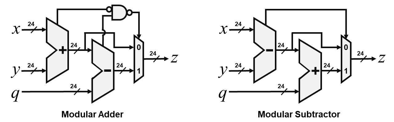
The modular arithmetic core consists of a 24-bit adder, a 24-bit subtractor and a 24-bit multiplier along with associated modular reduction logic. Our modular adder and subtractor designs are shown in Fig. 1, and the corresponding pseudo-codes are shown in Algorithms 2 and 3. Both designs use a pair of adder and subtractor, with the sum, carry bit, difference and borrow bit denoted as , , and respectively. Modular reduction is performed using conditional subtraction and addition, which are computed in the same cycle to avoid timing side-channels. The synthesized areas of the adder and the subtractor are around 550 GE (gate equivalent) each in area.
For modular multiplication, we use a 24-bit multiplier followed by Barrett reduction [33] modulo a prime of size up to 24 bits. Barrett reduction does not exploit any special property of the modulus , thus making it ideal for supporting configurable moduli. Let be the 48-bit product to be reduced to , then Barrett reduction computes by estimating the quotient without performing any division, as shown in Algorithm 4. Barrett reduction involves two multiplications, one subtraction, one bit-shift and one conditional subtraction. The value of is approximated as , with the error of approximation being , therefore the reduction is valid as long as . Since , is set to be the smallest number such that . Typically, is very close to , that is, the bit-size of .
In order to understand the trade-offs between flexibility and efficiency in modular multiplication, we have implemented two different architectures of Barrett reduction logic: (1) with fully configurable modulus ( can be an arbitrary prime) and (2) with pseudo-configurable modulus ( belongs to a specific set of primes), as shown in Fig. 2.
Apart from the prime (which can be up to 24 bits), the fully configurable version requires two additional inputs and such that ( and are allowed to be up to 24 bits and 6 bits respectively). It consists of total 3 multipliers, as shown in Fig. 2a, the first two being used to compute and respectively. For obtaining , the bit-wise shift is implemented purely using combinational logic (multiplexers) because shifting bits sequentially in registers can be extremely inefficient in terms of power consumption. We assume that since is not larger than 24 bits, is typically not smaller than 8 bits and we know that . The third multiplier is used to compute , and a pair of subtractors is used to calculate and perform the final reduction step. All the steps are computed in a single cycle to avoid any potential timing side-channels. The design was synthesized at 100 MHz (with near-zero slack) and occupies around 11k GE area, which includes the area (around 4k GE) of the 24-bit multiplier used to compute .
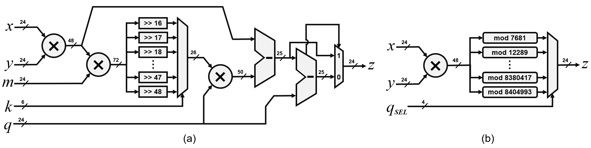
The pseudo-configurable modular multiplier implements Barrett reduction logic for the following primes used by NIST Round 1 lattice-based candidates: 7681 (CRYSTALS-Kyber) [26], 12289 (NewHope) [24], 40961 (R.EMBLEM) [34], 65537 (pqNTRUSign) [35], 120833 (Ding Key Exchange) [36], 133121 / 184321 (LIMA) [37], 8380417 (CRYSTALS-Dilithium) [27], 8058881 (qTESLA v1.0) and 4205569 / 4206593 / 8404993 (qTESLA v2.0) [25]. As shown in Fig. 2b, there is dedicated reduction block for each of these primes, and the input is used to select the output of the appropriate block while the inputs to the other blocks are data-gated to save power. Since the reduction blocks have the parameters , and coded in digital logic and do not require explicit multipliers, they involve lesser computation than the fully configurable reduction circuit from Fig. 2a, albeit at the cost of some additional area and decrease in flexibility. The reduction becomes particularly efficient when at least one of and or both can be written in the form , where are not more than four positive integers. For example, we consider the CRYSTALS primes: for we have and , and for we have and . Therefore, the multiplications by and can be converted to significantly cheaper bit-shifts and additions / subtractions, as shown in Algorithms 5 and 6. Implementation details and reduction parameters for each customized modular reduction block are provided in Appendix A. This design also performs modular multiplication in a single cycle. It was synthesized at 100 MHz (with near-zero slack) and occupies around 19k GE area, including the area of the 24-bit multiplier.
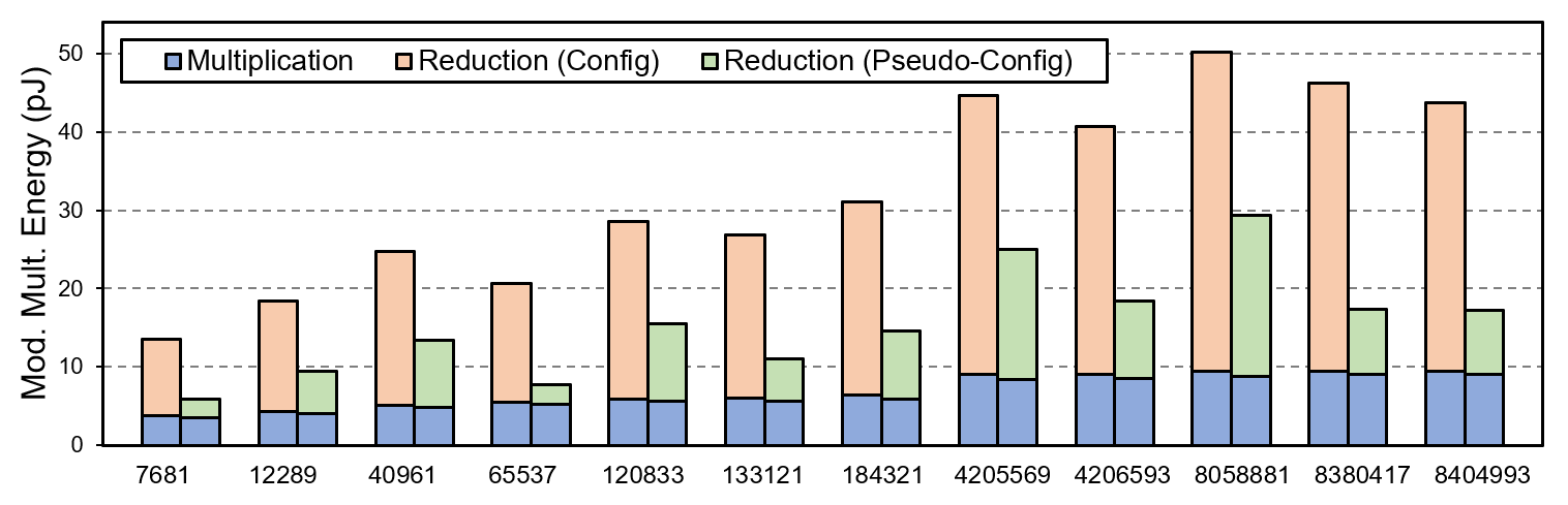
In Fig. 3, we compare the simulated energy consumption of the fully configurable and pseudo-configurable modular multiplier architectures for all the primes mentioned earlier. As expected, the multiplication itself consumes the same energy in both cases, but the modular reduction energy is up to lower for the pseudo-configurable design. The overall decrease in modular multiplication energy, considering both multiplication and reduction together, is up to , clearly highlighting the benefit of the dedicated modular reduction data-paths when working with prime moduli. For reduction modulo (), e.g., in the case of Frodo, the output of the 24-bit multiplier is simply bit-wise AND-ed with implying that the modular reduction energy is negligible.
3.2 Butterfly Unit and ALU
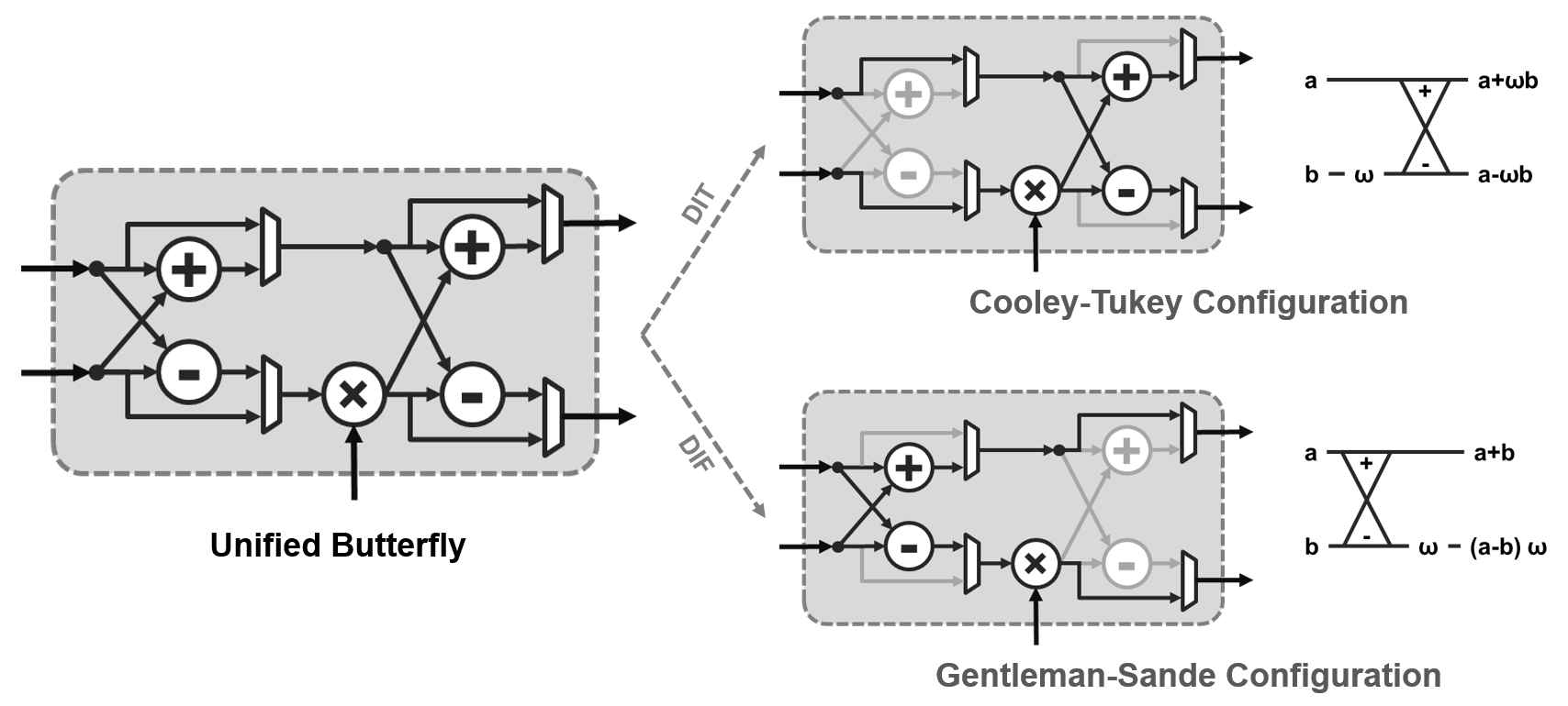
Next, we elaborate how the modular arithmetic units described earlier are integrated together to build the butterfly module. As discussed in Section 2, NTT computations involve butterfly operations similar to the Fast Fourier Transform, with the only difference being that all arithmetic is performed modulo instead of complex numbers. There are two butterfly configurations – Cooley-Tukey (or DIT) and Gentleman-Sande (or DIF). In terms of arithmetic, the DIT butterfly computes and the DIF butterfly computes , where and are the inputs to the butterfly and is the twiddle factor. The DIT butterfly requires inputs to be in bit-reversed order and the DIF butterfly generates outputs in bit-reversed order, thus making DIF and DIT suitable for NTT and INTT respectively. While software implementations have the flexibility to program both configurations, hardware designs typically implement either DIT or DIF, thus requiring bit-reversals. To solve this problem, we have implemented a unified butterfly architecture [38] which can be configured as both DIT and DIF, as shown in Fig. 4. It consists of two sets of modular adders and subtractors along with some multiplexing circuitry to select whether the multiplication with is performed before or after the addition and subtraction. Since the critical path of the design is inside the modular multiplier, there is no impact on system performance. The associated area overhead is also negligible.
The modular arithmetic blocks inside the butterfly are re-used for coefficient-wise polynomial arithmetic operations as well as for multiplying polynomials with the appropriate powers of and during negative-wrapped convolution. Apart from butterfly and arithmetic modulo , the Sapphire ALU also supports the following bit-wise operations – AND, OR, XOR, left shift and right shift.
3.3 NTT Memory Architecture
Hardware architectures for polynomial multiplication using NTT consist of memory banks for storing the polynomials along with the ALU which performs butterfly computations. Since each butterfly needs to read two inputs and write two outputs all in the same cycle, these memory banks are typically implemented using dual-port RAMs [9, 39, 30, 19] or four-port RAMs [17]. Although true dual-port memory is easily available in state-of-the-art commercial FPGAs in the form of block RAMs (BRAMs), use of dual-port SRAMs in ASIC can pose large area overheads in resource-constrained devices. Compared to a simple single-port SRAM, a dual-port SRAM has double the number of row and column decoders, write drivers and read sense amplifiers. Also, the bit-cells in a low-power dual-port SRAM consist of ten transistors (10T) compared to the usual six transistor (6T) bit-cells in a single-port SRAM [40]. Therefore, the area of a dual-port SRAM can be as much as double the area of a single-port SRAM with the same number of bits and column muxing. To reduce this area overhead, we implement an area-efficient NTT memory architecture [38] which uses the constant-geometry FFT data-flow [41] and consists of single-port SRAMs only.
The constant geometry NTT is described in Algorithm 7 [42, 39]. Clearly, the coefficients of the polynomial are accessed in the same order for each stage, thus simplifying the read/write control circuitry. For constant geometry DIT NTT, the butterfly inputs are and and the outputs are and , while the inputs are and and the outputs are and for DIF NTT. However, the constant geometry NTT is inherently out-of-place, therefore requiring storage for both polynomials and . For our hardware implementation, we create two memory banks – left and right – to store these two polynomials while allowing the butterfly inputs and outputs to ping-pong between them during each stage of the transform. Although out-of-place NTT requires storage for both the input and output polynomials, this does not affect the total memory requirements of the crypto-processor because the total number of polynomials required to be stored during the protocol execution is greater than two, e.g., four polynomials are involved in any computation of the form .
Next, we describe how these memory banks are constructed using single-port SRAMs so that each butterfly can be computed in a single cycle without causing read/write hazards. As shown in Fig. 5a, each polynomial is split among four single port SRAMs Mem 0-3 on the basis of the least and most significant bits (LSB and MSB) of the coefficient index (or address ). This allows simultaneously accessing coefficient index pairs of the form and . Our NTT memory architecture is shown in Fig. 5b, which consists of two such memory banks labelled as LWE Poly Cache. In every cycle, the butterfly inputs are read from two different single-port SRAMs (out of four SRAMs in the input memory bank) and the outputs are also written to two different single-port SRAMs (out of four SRAMs in the output memory bank), thus avoiding hazards. The data flow in the first two cycles of NTT is shown in Fig. 6, where the input polynomial is stored in the left bank and the output polynomial is stored in the right bank. As the input and output polynomials exchange their memory banks from one stage to the next, our NTT control circuitry ensures that the same data-flow is maintained. To illustrate this, the memory access patterns for all three stages of an 8-point NTT are shown in Fig. 7 for both decimation-in-time and decimation-in-frequency.
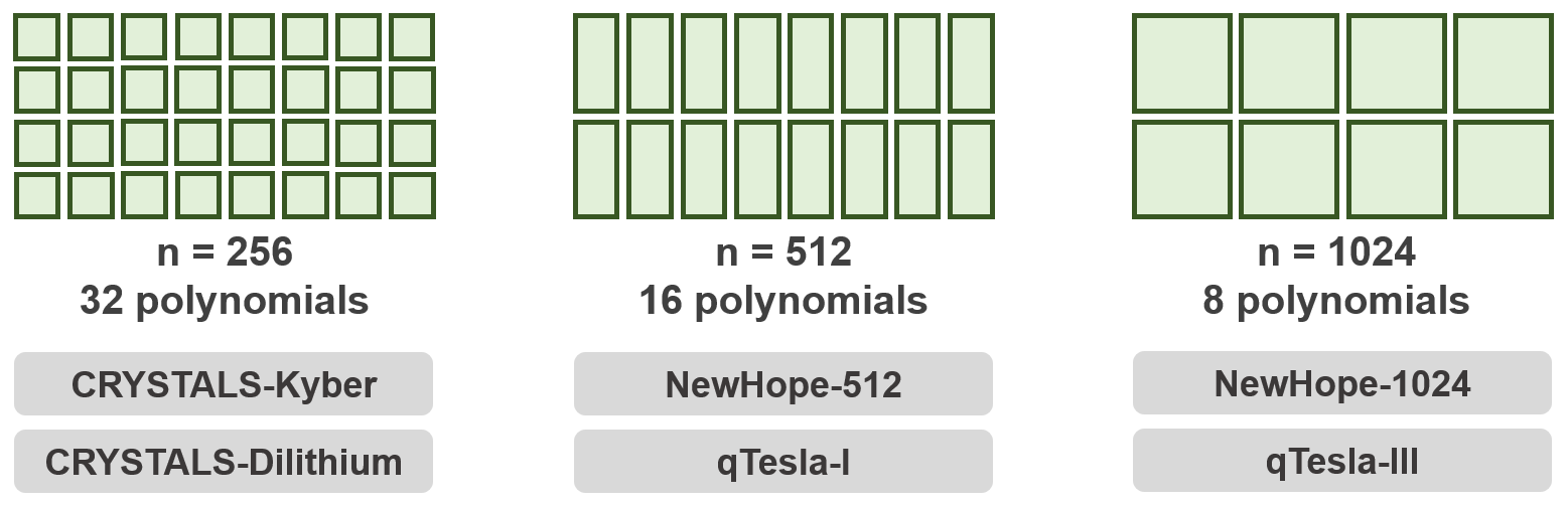
The two memory banks consist of four -bit single-port SRAMs each (24 KB total). Together they store 8192 entries, which can be split into four 2048-dimension polynomials or eight 1024-dimension polynomials or sixteen 512-dimension polynomials or thirty-two 256-dimension polynomials or sixty-four 128-dimension polynomials or one-hundred-twenty-eight 64-dimension polynomials. By constructing this memory using single-port SRAMs (and some additional read-data multiplexing circuitry), we have achieved area savings equivalent to 124k GE compared to a dual-port SRAM-based implementation. This is particularly important since SRAMs account for a large portion of the total hardware area in ASIC implementations of lattice-based cryptography [17, 43].
In order to allow configurable parameters, our NTT hardware also requires additional storage (labelled as NTT Constants RAM in Fig. 5) for the pre-computed twiddle factors: , for and and , for . Since and , this would require another 24 KB of memory. To reduce this overhead, we exploit the following properties of and : , and [30]. Then, it’s sufficient to store only for and , for , thus reducing the twiddle factor memory size by 37.5% down to 15 KB.
Finally, we compare the energy-efficiency and performance of our NTT with state-of-the-art software and ASIC hardware implementations in Table 1. For the software implementation, we have used assembly-optimized code for ARM Cortex-M4 from the PQM4 crypto library [44], and measurements were performed using the NUCLEO-F411RE development board [45]. Total cycle count of our NTT is , including the multiplication of polynomial coefficients with powers of . All measurements for our NTT implementation were performed on our test chip operating at clock frequency 72 MHz and nominal supply voltage 1.1 V. Our hardware-accelerated NTT is up to more energy-efficient than the software implementation, after accounting for voltage scaling. It is more energy-efficient compared to the fast NTT design from [14] with similar cycle count, and more energy-efficient compared to the slow NTT design from [14] with cycle count. Our NTT is almost twice as fast as [43], since our memory architecture allows computing one butterfly per cycle even with single-port SRAMs, while having similar energy consumption. The energy-efficiency of our NTT implementation is largely due to the careful design of low-power modular arithmetic, as discussed earlier, which decreases overall modular reduction complexity and simplifies the logic circuitry. However, our NTT is still about less energy-efficient compared to [17], primarily due to the fact that [17] uses 16 parallel butterfly units along with dedicated four-port scratch-pad buffers to achieve higher parallelism and lower energy consumption at the cost of significantly larger chip area (2.05 mm2) compared to our design (0.28 mm2). As will be discussed in Section 6, sampling accounts for majority of the computational cost in Ring-LWE and Module-LWE schemes, therefore justifying our choice of area-efficient NTT architecture at the cost of some energy overhead.
| Design | Platform | Tech | VDD | Freq | Parameters | NTT | NTT |
| (nm) | (V) | (MHz) | Cycles | Energy | |||
| This work | ASIC | 40 | 1.1 | 72 | 1,289 | 165.98 nJ | |
| 2,826 | 410.52 nJ | ||||||
| 6,155 | 894.28 nJ | ||||||
| Software [44] | ARM Cortex-M4 | - | 3.0 | 100 | 22,031 | 13.55 J | |
| 34,262 | 21.07 J | ||||||
| 75,006 | 46.13 J | ||||||
| Song et al. [17] | ASIC | 40 | 0.9 | 300 | 160 | 31 nJ | |
| 492 | 96 nJ | ||||||
| Nejatollahi et al. [14] | ASIC | 45 | 1.0 | 100 | 2,854 | 1016.02 nJ | |
| 11,053 | 596.86 nJ | ||||||
| Fritzmann et al. [43] | ASIC | 65 | 1.2 | 25 | 2,056 | 254.52 nJ | |
| 4,616 | 549.98 nJ | ||||||
| 10,248 | 1205.03 nJ | ||||||
| Roy et al. [9] | FPGA | - | - | 313 | 1,691 | - | |
| 278 | 3,443 | - | |||||
| Du et al. [30] | FPGA | - | - | 233 | 4,066 | - | |
| 8,806 | - |
4 Discrete Distribution Sampler
Hardness of the LWE problem is directly related to statistical properties of the error samples. Therefore, an accurate and efficient sampler is a critical component of any lattice cryptography implementation. Sampling accounts for a major portion of the computational overhead in software implementations of ideal and module lattice-based protocols [46]. A cryptographically secure pseudo-random number generator (CS-PRNG) is used to generate uniformly random numbers, which are then post-processed to convert them into samples from different discrete probability distributions. In this section, we describe our design of energy-efficient CS-PRNG along with fast sampling techniques for configurable distribution parameters.
4.1 Energy-Efficient CS-PRNG
| PRNG | Area (kGE) a | Cycles / | No. of | Energy |
| Round | PRNG Bits | (pJ/bit) b | ||
| SHAKE-128 | 34.5 (23.5) | 24 | 1344 | 1.67 |
| SHAKE-256 | 1088 | 2.07 | ||
| ChaCha20 | 21.1 (17.5) | 20 | 512 | 3.53 |
| AES-128-CTR | 15.0 (11.1) | 11 | 128 | 5.10 |
| AES-256-CTR | 15 | 128 | 7.56 | |
| a Area of placed-and-routed design (post-synthesis area in brackets) | ||||
| b Energy measured from test chip operating at 1.1 V | ||||
Some of the standard choices for CS-PRNG are SHA-3 in the SHAKE mode [47], AES in counter mode [48] and ChaCha20 [49]. In order to identify the most efficient among these, we have compared them in terms of area, pseudo-random bit generation performance and energy consumption, as shown in Table 2. Only place-and-route area and measured energy are considered for all analysis, and synthesis area is reported for reference. For fair comparison, all the three primitives – SHA-3, AES and ChaCha20 – were implemented as full data path architectures. From Fig. 8, we observe that although all three primitives have comparable area-energy product, SHA-3 is more energy-efficient than ChaCha20 and more energy-efficient than AES; and this is largely due to the fact that SHA-3 generates the highest number of pseudo-random bits per round.
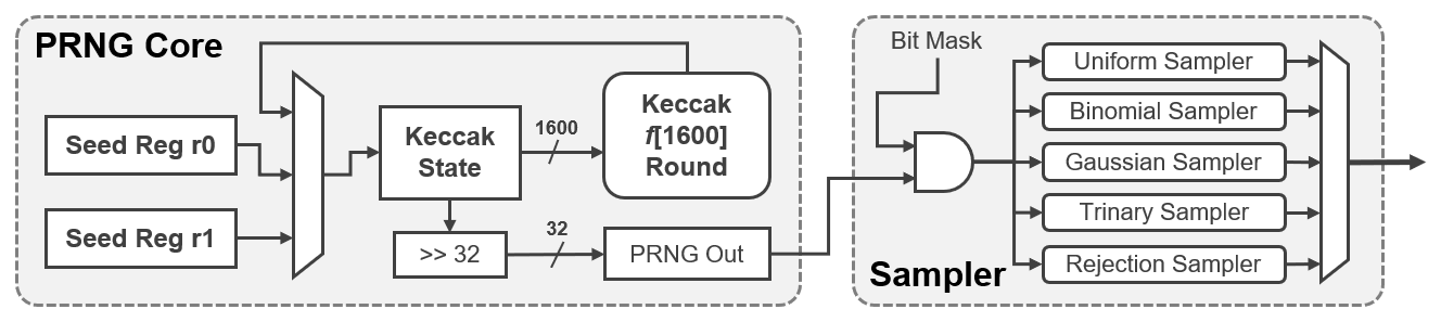
The basic building block of SHA-3 is the Keccak permutation function [50]. Therefore, our PRNG consists of a 24-cycle Keccak-f[1600] core [38] which can be configured in different SHA-3 modes and consumes 2.33 nJ per round at nominal voltage of 1.1 V (and 0.89 nJ per round at 0.68 V). Its 1600-bit state is processed in parallel, thus avoiding expensive register shifts and multiplexing required in serial architectures. Fig. 9 shows the overall architecture our discrete distribution sampler with the energy-efficient SHA-3 core. Pseudo-random bits generated by SHAKE-128 or SHAKE-256 are stored in the 1600-bit Keccak state register, and shifted out 32 bits at a time as required by the sampler. The sampler then feeds these bits, AND-ed with the appropriate bit mask to truncate them to desired size, to the post-processing logic to perform one of the following five types of operations – rejection sampling in , binomial sampling with standard deviation , discrete Gaussian sampling with standard deviation and desired precision up to 32 bits, uniform sampling in for and trinary sampling in with specified weights for the and samples.
4.2 Rejection Sampling
The public polynomial in Ring-LWE and the public vector in Module-LWE have their coefficients uniformly drawn from through rejection sampling, where uniformly random numbers of desired bit size are obtained from the PRNG as candidate samples and only numbers smaller than are accepted. The probability that a random number is not accepted is known as the rejection probability.
| Prime | Bit | Rej. Prob. | Scaling | Rej. Prob. | Decrease in |
| Size | (w/o. scaling) | Factor | (w. scaling) | Rej. Prob. | |
| 7681 | 13 | 0.06 | 1 | 0.06 | - |
| 12289 | 14 | 0.25 | 5 | 0.06 | 0.19 |
| 40961 | 16 | 0.37 | 3 | 0.06 | 0.31 |
| 65537 | 17 | 0.50 | 7 | 0.12 | 0.38 |
| 120833 | 17 | 0.08 | 1 | 0.08 | - |
| 133121 | 18 | 0.49 | 7 | 0.11 | 0.38 |
| 184321 | 18 | 0.30 | 11 | 0.03 | 0.27 |
| 8380417 | 23 | 0 | 1 | 0 | - |
| 8058881 | 23 | 0.04 | 1 | 0.04 | - |
| 4205569 | 23 | 0.50 | 7 | 0.12 | 0.38 |
| 4206593 | 23 | 0.50 | 7 | 0.12 | 0.38 |
| 8404993 | 24 | 0.50 | 7 | 0.12 | 0.38 |
For prime , the rejection probability is calculated as . In Table 3, we list the rejection probabilities for primes mentioned earlier in Section 3. Clearly, different primes have very different rejection probabilities, often as high as 50%, which can be a bottleneck in lattice-based protocols. To solve this problem, we refer to [51] where pseudo-random numbers smaller than are accepted for , thus reducing the rejection probability from 25% to 6%. We extend this technique for any prime by scaling the rejection bound from to , for appropriate small integer , so that the rejection probability is now . We list these scaling factors for the primes in Table 3 along with the corresponding decrease in rejection probability.
| Design | Platform | Tech | VDD | Freq | Parameters | Samp. | Samp. |
| (nm) | (V) | (MHz) | Cycles | Energy | |||
| This work | ASIC | 40 | 1.1 | 72 | 461 | 50.90 nJ | |
| 921 | 105.74 nJ | ||||||
| 1,843 | 211.46 nJ | ||||||
| Software [44] | ARM Cortex-M4 | - | 3.0 | 100 | 60,433 | 37.17 J | |
| 139,153 | 85.58 J | ||||||
| 284,662 | 175.07 J |
Although this method reduces rejection rates, the output samples now lie in instead of . In [51], for and , the accepted samples are reduced to by subtracting from them up to four times. Since is not fixed for our rejection sampler, we employ Barrett reduction [33] for this purpose. Unlike modular multiplication, where the inputs lie in , the inputs here are much smaller; so the Barrett reduction parameters are also quite small, therefore requiring little additional logic. In Table 4, we compare our rejection sampler performance (SHAKE-128 used as PRNG) with software implementation on ARM Cortex-M4 using assembly-optimized Keccak [44].
4.3 Binomial Sampling
| Design | Platform | Tech | VDD | Freq | Parameters | Samp. | Samp. |
| (nm) | (V) | (MHz) | Cycles | Energy | |||
| This work | ASIC | 40 | 1.1 | 72 | 505 | 58.20 nJ | |
| 1,009 | 116.26 nJ | ||||||
| 2,018 | 232.50 nJ | ||||||
| Software [44] | ARM Cortex-M4 | - | 3.0 | 100 | 52,603 | 32.35 J | |
| 155,872 | 95.86 J | ||||||
| 319,636 | 196.58 J | ||||||
| Song et al. [17] | ASIC | 40 | 0.9 | 300 | 3,704 | 1.25 J | |
| Oder et al. [13] | FPGA | - | - | 125 | 33,792 | - |
For binomial sampling, we take two -bit chunks from the PRNG and computes the difference of their Hamming weights, as proposed in [24]. The resulting samples follow a binomial distribution with standard deviation . We allow configuring to any value up to 32, thus providing the flexibility to support different standard deviations.
We compare our binomial sampling performance (SHAKE-256 used as PRNG) with state-of-the-art software and hardware implementations in Table 5. Our sampler is more than two orders of magnitude more energy-efficient compared to the software implementation on ARM Cortex-M4 which uses assembly-optimized Keccak [44]. It is also more efficient than [17] which uses Knuth-Yao sampling [52] for binomial distributions with ChaCha20 as PRNG.
4.4 Discrete Gaussian Sampling
Our discrete Gaussian sampler implements the inversion method of sampling [53] from a discrete symmetric zero-mean distribution on with small support which approximates a rounded continuous Gaussian distribution, e.g., in Frodo [23] and R.EMBLEM [34]. For a distribution with support , where is a small positive integer, the probabilities for , such that can be derived from the cumulative distribution table (CDT) , where and for for precision . Given random inputs and distribution table , a sample from can be obtained using Algorithm 8 [23].
The sampling must be constant-time in order to eliminate timing side-channels, therefore the algorithm does a complete loop through the entire table . The comparison must also be implemented in a constant-time manner. Our implementation adheres to these requirements and uses a RAM to store the CDT, allowing the parameters and to be configured according to the choice of the distribution. In Table 6, we have compared our Gaussian sampler performance (SHAKE-256 used as PRNG) with software implementation on ARM Cortex-M4 using assembly-optimized Keccak [44], and we observe up to improvement in energy-efficiency after accounting for voltage scaling. Hardware architectures for Knuth-Yao sampling have been proposed by [9] and [17], but they are for discrete Gaussian distributions with larger standard deviation and higher precision, which we do not support.
| Design | Platform | Tech | VDD | Freq | Parameters | Samp. | Samp. |
| (nm) | (V) | (MHz) | Cycles | Energy | |||
| This work | ASIC | 40 | 1.1 | 72 | 29,169 | 1232.71 nJ | |
| 15,330 | 647.86 nJ | ||||||
| 14,306 | 604.58 nJ | ||||||
| Software [44] | ARM Cortex-M4 | - | 3.0 | 100 | 397,921 | 244.72 J | |
| 325,735 | 200.33 J | ||||||
| 317,541 | 195.29 J |
4.5 Other Distributions
Several lattice-based protocols, such as CRYSTALS-Dilithium [27] and qTESLA [25], require polynomials to be sampled with coefficients uniformly distributed in the range for a specified bound . For this, we again use rejection sampling. Unlike rejection sampling from , we do not require any special techniques since is typically small or an integer close to a power of two.
Finally, we have also implemented a trinary sampler for polynomials with coefficients from . We classify these polynomials into three categories: (1) with non-zero coefficients, (2) with ’s and ’s, and (3) with coefficients distributed as and for . Their implementations are described in Algorithms 9, 10 and 11. For the first two cases, we start with a zero-polynomial of size . Then, uniformly random coefficient indices are generated, and the corresponding coefficients are replaced with or if they are zero [25, 35]. For the third case, sampling of the coefficients is based on the observation [54] that for a uniformly random number we have , and . Therefore, for the appropriate value of , we can generate samples from the desired trinary distribution with . For all three algorithms, the symbol denotes pseudo-random number generation using the PRNG.
5 Chip Architecture
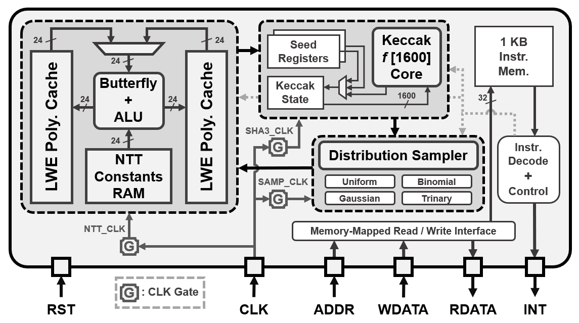
The top-level architecture of Sapphire is shown in Fig. 10. The efficient building blocks described in Sections 3 and 4 are integrated with a 1 KB instruction memory and an instruction decoder to form the core of our crypto-processor. It can be programmed using 32-bit custom instructions to perform different polynomial arithmetic, transform and sampling operations, as well as simple branching. For example, the following instructions generate polynomials , and calculate , which is a typical computation in the Ring-LWE-based scheme NewHope-1024:
config (n = 1024, q = 12289)
# sample_a
rej_sample (prng = SHAKE-128, seed = r0, c0 = 0, c1 = 0, poly = 0)
# sample_s
bin_sample (prng = SHAKE-256, seed = r1, c0 = 0, c1 = 0, k = 8, poly = 1)
# sample_e
bin_sample (prng = SHAKE-256, seed = r1, c0 = 0, c1 = 1, k = 8, poly = 2)
# ntt_s
mult_psi (poly = 1)
transform (mode = DIF_NTT, poly_dst = 4, poly_src = 1)
# a_mul_s
poly_op (op = MUL, poly_dst = 0, poly_src = 4)
# intt_a_mul_s
transform (mode = DIT_INTT, poly_dst = 5, poly_src = 0)
mult_psi_inv (poly = 5)
# a_mul_s_plus_e
poly_op (op = ADD, poly_dst = 1, poly_src = 5)
The config instruction is first used to configure the protocol parameters and which, in this example, are the parameters from NewHope-1024. For , the polynomial cache is divided into 8 polynomials, which are accessed using the poly argument in all instructions. For sampling, the seed can be chosen from a pair of 256-bit registers r0 and r1, while two 16-bit registers c0 and c1 are used as counters for sampling multiple polynomials from the same seed. For coefficient-wise operations poly_op, the poly_src argument indicates the first source polynomial while the poly_dst argument is used to denote the second source (and destination) polynomial. Similarly, the following set of instructions are used to generate matrix of polynomials and vectors of polynomials , and calculate , which is a typical computation in the Module-LWE-based scheme CRYSTALS-Kyber-512:
config (n = 256, q = 7681)
# sample_s
bin_sample (prng = SHAKE-256, seed = r1, c0 = 0, c1 = 0, k = 3, poly = 4)
bin_sample (prng = SHAKE-256, seed = r1, c0 = 0, c1 = 1, k = 3, poly = 5)
# sample_e
bin_sample (prng = SHAKE-256, seed = r1, c0 = 0, c1 = 2, k = 3, poly = 24)
bin_sample (prng = SHAKE-256, seed = r1, c0 = 0, c1 = 3, k = 3, poly = 25)
# ntt_s
mult_psi (poly = 4)
transform (mode = DIF_NTT, poly_dst = 16, poly_src = 4)
mult_psi (poly = 5)
transform (mode = DIF_NTT, poly_dst = 17, poly_src = 5)
# sample_A0
rej_sample (prng = SHAKE-128, seed = r0, c0 = 0, c1 = 0, poly = 0)
rej_sample (prng = SHAKE-128, seed = r0, c0 = 1, c1 = 0, poly = 1)
# A0_mul_s
poly_op (op = MUL, poly_dst = 0, poly_src = 16)
poly_op (op = MUL, poly_dst = 1, poly_src = 17)
init (poly = 20)
poly_op (op = ADD, poly_dst = 20, poly_src = 0)
poly_op (op = ADD, poly_dst = 20, poly_src = 1)
# sample_A1
rej_sample (prng = SHAKE-128, seed = r0, c0 = 0, c1 = 1, poly = 0)
rej_sample (prng = SHAKE-128, seed = r0, c0 = 1, c1 = 1, poly = 1)
# A1_mul_s
poly_op (op = MUL, poly_dst = 0, poly_src = 16)
poly_op (op = MUL, poly_dst = 1, poly_src = 17)
init (poly = 21)
poly_op (op = ADD, poly_dst = 21, poly_src = 0)
poly_op (op = ADD, poly_dst = 21, poly_src = 1)
# intt_A_mul_s
transform (mode = DIT_INTT, poly_dst = 8, poly_src = 20)
mult_psi_inv (poly = 8)
transform (mode = DIT_INTT, poly_dst = 9, poly_src = 21)
mult_psi_inv (poly = 9)
# A_mul_s_plus_e
poly_op (op = ADD, poly_dst = 24, poly_src = 8)
poly_op (op = ADD, poly_dst = 25, poly_src = 9)
In this example, parameters from CRYSTALS-Kyber-512 have been used. For , the polynomial cache is divided into 32 polynomials, which are again accessed using the poly argument. The init instruction is used to initialize a specified polynomial with all zero coefficients. The matrix is generated one row at a time, following a just-in-time approach [55] instead of generating and storing all the rows together, to save memory, which becomes especially useful when dealing with larger matrices such as in CRYSTALS-Kyber-1024 and CRYSTALS-Dilithium-IV. We have written a Perl script to parse such plain-text programs and convert them into 32-bit binary instructions which can be decoded by the Sapphire crypto-processor. A complete list of supported instructions is provided in Appendix B.
We use dedicated clock gates for fine-grained power savings during program execution, and an interrupt pin is used to indicate completion of the program. Its memory and data registers can be accessed through a simple memory-mapped interface. Using the same interface, it is also coupled with a low-power RISC-V micro-processor [56], with 32 KB instruction memory and 64 KB data memory, which implements the RV32IM instruction set [57] and has Dhrystone performance similar to ARM Cortex-M0. When executing cryptographic workloads in the Sapphire core, the RISC-V core can be clock-gated using the wait-for-interrupt (wfi) instruction. The processor is woken up by a dedicated interrupt from the Sapphire core, which is raised when the cryptographic operation is complete. Using the memory-mapped interface ensures that the cryptographic core can be accessed through simple load and store instructions, without requiring any custom instructions or changes to the compilation toolchain. While the cryptographic core is used to accelerate all lattice cryptography computations, the RISC-V processor is used for scheduling the cryptographic workloads as well as for compression and decompression of public keys and ciphertexts. The Keccak-f[1600] core inside Sapphire can be accessed standalone through RISC-V software, and is used to accelerate SHA-3 hashing and extendable output functions according to the requirements of the protocol.
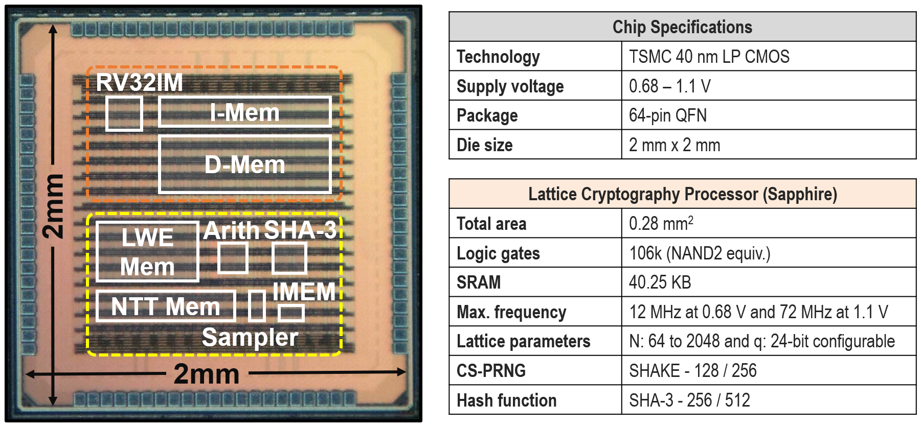
Our test chip was fabricated in the TSMC 40nm LP CMOS process, and the chip micrograph is shown in Fig. 11 with the key design components highlighted. The final placed-and-routed design of our Sapphire core consists of 106k logic gates (76 kGE for synthesized design) and 40.25 KB SRAM, with a total area of 0.28 mm2 (logic and memory combined). Our test chip supports supply voltage scaling from 0.68 V to 1.1 V. Although one of our key design objectives was to demonstrate a configurable lattice cryptography processor, our architecture can be easily scaled for more specific parameter sets. For example, in order to accelerate only NewHope-512 (), size of the polynomial cache can be reduced to 6.5 KB ( bits) and the pre-computed NTT constants can be hard-coded in logic or stored in a 2.03 KB ROM ( bits) instead of the 15 KB SRAM. Also, the modular arithmetic logic in the ALU can be simplified significantly to work with a single prime only.
We use the on-chip software-configurable clock gates (shown in Fig. 10) to accurately measure power consumption of different sub-modules inside the Sapphire core, e.g., sampling, NTT, arithmetic, etc. For example, the following instructions are executed to measure the average power consumption of NTT over 1000 executions:
clock_config (keccak = GATE, ntt = UNGATE, sampler = GATE)
c0 = 0
loop: mult_psi (poly = 0)
transform (mode = DIF_NTT, poly_dst = 4, poly_src = 0)
c0 = c0 + 1
flag = compare (c0, 1000)
if (flag == -1) goto loop
The clock_config instruction is used to control the clock gates, e.g., the PRNG and sampler clocks are gated when measuring NTT power (the RISC-V core is clock-gated using wfi as explained earlier). A simple loop is implemented using labels, comparison and conditional jump instructions, similar to assembly programs in general-purpose micro-controllers (please refer to Appendix B for details of our custom instructions). One of the chip GPIO pins is kept high during the execution of this program to indicate the measurement window, and the power consumption is measured using a source meter. This still includes leakage power from the rest of the chip, but it is only a small fraction of the total power compared to the dynamic power of the operation being measured. Similarly, power consumption of the RISC-V core is measured by clock-gating the Sapphire cryptographic core through software. Finally, leakage power of the chip is measured by externally gating the clock signal being supplied to the chip, so that all logic inside the chip is inactive.
The RISC-V processor consumes 45 W/MHz at 1.1 V (18 W/MHz at 0.68 V) when running the Dhrystone 2.1 benchmark. Power consumption of the cryptographic core is a strong function of the protocols being executed along with the associated parameters. Average power consumption of the lattice crypto-processor was measured to be around 8 mW at 1.1 V and 72 MHz (520 W at 0.68 V and 12 MHz). Total leakage power of the chip was measured to be 391 W at 1.1 V (70 W at 0.68 V). Since our chip operates on a single power domain, it is not possible to measure leakage power of different components of the chip. We report the individual module-wise leakage and dynamic power consumption, as obtained from post-place-and-route simulations of our design operating at 1.1 V and 72 MHz, in the table below:
| Module | P (W) | P (W) | P (W) |
|---|---|---|---|
| Butterfly + ALU | 18.28 | 9210.04 | 9228.32 |
| LWE Polynomial Cache | 120.28 | 1660.18 | 1780.46 |
| NTT Constants RAM | 76.50 | 661.61 | 738.11 |
| Keccak Core + Sampler | 41.15 | 1053.58 | 1094.73 |
| RISC-V Processor + Memory | 320.15 | 2745.68 | 3065.83 |
Before moving on to the protocol implementations and measurements, we summarize some key architectural design techniques we have used to achieve energy-efficiency:
-
•
We have employed increased parallelism in the modular arithmetic and CS-PRNG modules in the form of single-cycle butterfly computation and 1600-bit 24-cycle Keccak data-path respectively. This reduces cycle count as well as data movement and control circuitry, thus decreasing overall energy consumption.
-
•
Based on overall computational complexity, we know that additions are much cheaper than multiplications. Therefore, we have exploited special properties of prime and parameter , wherever possible, during Barrett reduction to convert expensive multiplications into cheaper bit-shifts and additions / subtractions.
-
•
Reading data from registers involves much smaller energy consumption compared to reading from SRAMs. We have used registers for storing PRNG seeds, temporary values and the Keccak state, and SRAMs are used to store only the polynomials. This significantly reduces overall energy consumption, especially for the Keccak core.
-
•
Software-controlled clock gates (explicitly inserted in RTL, apart from tool-inserted clock gates) for the sampler, PRNG and NTT allow fine-grained dynamic power savings by gating inactive modules as required during program execution.
-
•
The crypto-processor internal memory is efficiently utilized to store polynomials during protocol execution, thus avoiding access to the main processor’s data memory as much as possible and reducing energy consumption.
6 Protocol Implementations and Measurement Results
To measure the efficiency of our design, we have implemented the following NIST Round 2 lattice-based cryptography protocols on our test chip:
| Algorithm | Lattice Prob. | NIST Sec. | Parameter Set |
| CCA-KEM Algorithms | |||
| NewHope | Ring-LWE | 1 | NewHope-512 |
| 5 | NewHope-1024 | ||
| CRYSTALS-Kyber | Module-LWE | 1 | Kyber-512 |
| 3 | Kyber-768 | ||
| 5 | Kyber-1024 | ||
| Frodo | LWE | 1 | Frodo-640 |
| 3 | Frodo-976 | ||
| 5 | Frodo-1344 | ||
| Signature Algorithms | |||
| qTESLA | Ring-LWE | 1 | qTESLA-I |
| 3 | qTESLA-III-size | ||
| 3 | qTESLA-III-speed | ||
| CRYSTALS-Dilithium | Module-LWE | 1 | Dilithium-II |
| 2 | Dilithium-III | ||
| 3 | Dilithium-IV | ||
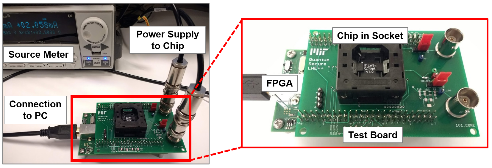
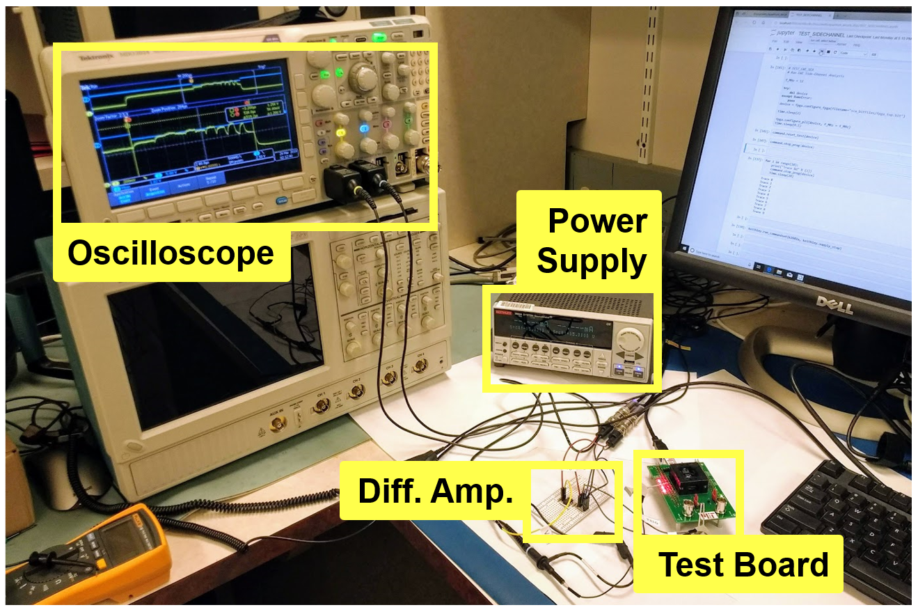
where NIST security levels 1-6 indicate brute-force security matching or exceeding that of AES-128, SHA3-256, AES-192, SHA3-384, AES-256 and SHA3-512 respectively. Fig. 12 shows our test board and measurement setup. The test chip is housed in a QFN64 socket soldered to the board, an Opal Kelly XEM7001 FPGA development board is used to interface with the chip, and a Keithley 2602A source meter supplies power to the chip. Both the FPGA and the source meter are controlled from a host computer through USB and GPIB interfaces respectively. The FPGA is used to transfer programs from the host computer to the instruction memory of our test chip. Also, a small ring-oscillator-based true random number generator [58] implemented on the FPGA is connected to our test chip through GPIO pins for providing fresh random inputs to the randombytes function which is part of the NIST API. All lattice cryptography programs are written using custom instructions and compiled with our script, while all RISC-V software is written in C and compiled using the riscv-gcc toolchain.
6.1 Protocol Implementations and Evaluation Results
Next, we describe some key aspects of our protocol implementations along with timing and energy profiling results. All polynomial arithmetic, transforms and sampling operations are accelerated using custom programs running in the Sapphire core, and all SHA-3 computations utilize the Keccak core inside Sapphire. The RISC-V processor is used only to read / write data and programs from / to the cryptographic core (both when executing polynomial computations and when utilizing the fast Keccak core for SHA-3 operations), generate initial randomness using the randombytes function, encode / decode messages and compress / decompress public keys and ciphertexts. For polynomials which need to be read from the polynomial cache and encoded (or decoded and written to the polynomial cache), we directly post-process the outputs (or pre-process the inputs) of the crypto-processor’s internal memory, instead of first storing the data in intermediate temporary arrays and then processing them. This saves around 10-20% cycles in overall protocol run-time. Also, the internal clock gates are strategically enabled and disabled during program execution using the clock_config instruction (please refer to Appendix B for details of our custom instructions) to reduce overall energy consumption.
For the NewHope and CRYSTALS-Kyber key exchange schemes, each of the CPA-secure public key encryption functions – CPA-PKE.KeyGen, CPA-PKE.Encrypt and CPA-PKE.Decrypt – has been written entirely (excluding the encoding and decoding operations) using Sapphire custom instructions with each of the corresponding programs fitting completely in its 1 KB instruction memory. The CCA-secure key encapsulation functions – CCA-KEM.KeyGen, CCA-KEM.Encaps and CCA-KEM.Decaps – involve calls to SHA-3 and the CPA-PKE functions (according to the Fujisaki-Okamoto transform [59]), which are implemented in software. Since the signature schemes qTESLA and CRYSTALS-Dilithium both involve probabilistic rejection of intermediate values, the associated polynomial computations are split into multiple custom programs instead of one each for the KeyGen, Sign and Verify functions. These blocks of code are scheduled using RISC-V software, which also handles encoding and decoding operations. The only exception is the KeyGen step in qTESLA, where high-precision discrete Gaussian sampling using large CDT tables is implemented in software, with the SHA-3 functions accelerated in hardware.
Since Module-LWE algorithms involve working with vectors or matrices of polynomials, it is particularly important to ensure that these polynomials fit inside the crypto-processor memory as much as possible (because reads and writes to the internal memory through software are not cheap). When multiplying the public matrix A with the secret vector s, the matrix A is generated through rejection sampling, one row at a time, following the just-in-time approach from [55]. This reduces memory footprint so that the entire computation can fit in the polynomial cache.
| Protocol | Cortex-M4 [44] | This work | |||
|---|---|---|---|---|---|
| Cycles | Energy (J) | Cycles | Power (mW) | Energy (J) | |
| NewHope-512-CPA-PKE | |||||
| KeyGen | - | - | 18,667 | 7.15 | 1.85 |
| Encrypt | - | - | 53,499 | 7.79 | 5.79 |
| Decrypt | - | - | 29,099 | 6.81 | 2.77 |
| NewHope-1024-CPA-PKE | |||||
| KeyGen | 1,179,353 | 725.30 | 38,012 | 7.39 | 3.90 |
| Encrypt | 1,663,023 | 1022.76 | 106,611 | 8.10 | 12.00 |
| Decrypt | 194,439 | 119.58 | 56,061 | 9.31 | 7.26 |
| CRYSTALS-Kyber-512-CPA-PKE | |||||
| KeyGen | 609,923 | 375.10 | 46,187 | 7.61 | 4.90 |
| Encrypt | 721,925 | 443.98 | 66,851 | 8.33 | 7.74 |
| Decrypt | 95,894 | 58.97 | 32,198 | 7.67 | 3.45 |
| CRYSTALS-Kyber-768-CPA-PKE | |||||
| KeyGen | 1,001,328 | 615.82 | 72,245 | 7.40 | 7.43 |
| Encrypt | 1,116,540 | 686.67 | 94,440 | 7.87 | 10.31 |
| Decrypt | 129,560 | 79.68 | 40,202 | 7.75 | 4.34 |
| CRYSTALS-Kyber-1024-CPA-PKE | |||||
| KeyGen | 1,610,114 | 990.22 | 100,453 | 7.95 | 11.09 |
| Encrypt | 1,747,687 | 1074.83 | 124,142 | 7.94 | 13.70 |
| Decrypt | 162,204 | 99.76 | 48,205 | 8.42 | 5.65 |
| Includes program execution and read/write from/to crypto-processor | |||||
In Table 7, we compare cycle count and energy consumption of our implementations of the Ring-LWE and Module-LWE CPA-PKE schemes with assembly-optimized software on ARM Cortex-M4 micro-processor (from PQM4 [44]), with average cycle counts for 100 executions. The energy consumption of our test chip has been measured at 1.1 V and 72 MHz, while the energy consumption of the Cortex-M4 processor is estimated from cycle counts using average power (61.5 mW or 615 pJ/cycle at 3.0 V and 100 MHz) measured on NUCLEO-F411RE operating at 100 MHz. The cycle count and energy consumption for our implementation include program execution as well as the additional overhead of writing inputs to and reading outputs from the Sapphire cryptographic core. For both NewHope and CRYSTALS-Kyber, we observe up to an order of magnitude improvement in energy-efficiency compared to software, after accounting for voltage scaling. Fig. 13 shows how configurability of the Sapphire polynomial cache is utilized to support different ring dimensions.
Although our lattice crypto-processor architecture primarily targets Ring-LWE and Module-LWE schemes, we also implement the LWE-based Frodo KEM protocol to demonstrate its flexibility. Since LWE-based algorithms require large matrix multiplications, the arithmetic operations dominate total computation cost unlike Ring-LWE and Module-LWE where sampling is the most expensive operation. Since the matrix dimensions are not powers of two, we tile the rows or columns so that we can use the crypto-processor’s array operations effectively, as shown in Fig. 14. For Frodo-640, we split each 640-element array into two arrays of size 512 and 128. For Frodo-976, we simply use arrays of size 1024 with the last 48 elements zeroed out or ignored, as applicable. For Frodo-1344, we use arrays of size 1536, formed by splitting them into two arrays of size 1024 and 512, with the last 192 elements (of the 512-dimension array) zeroed out or ignored, as applicable. However, this tiling scheme makes our version of Frodo incompatible with the reference software implementation.
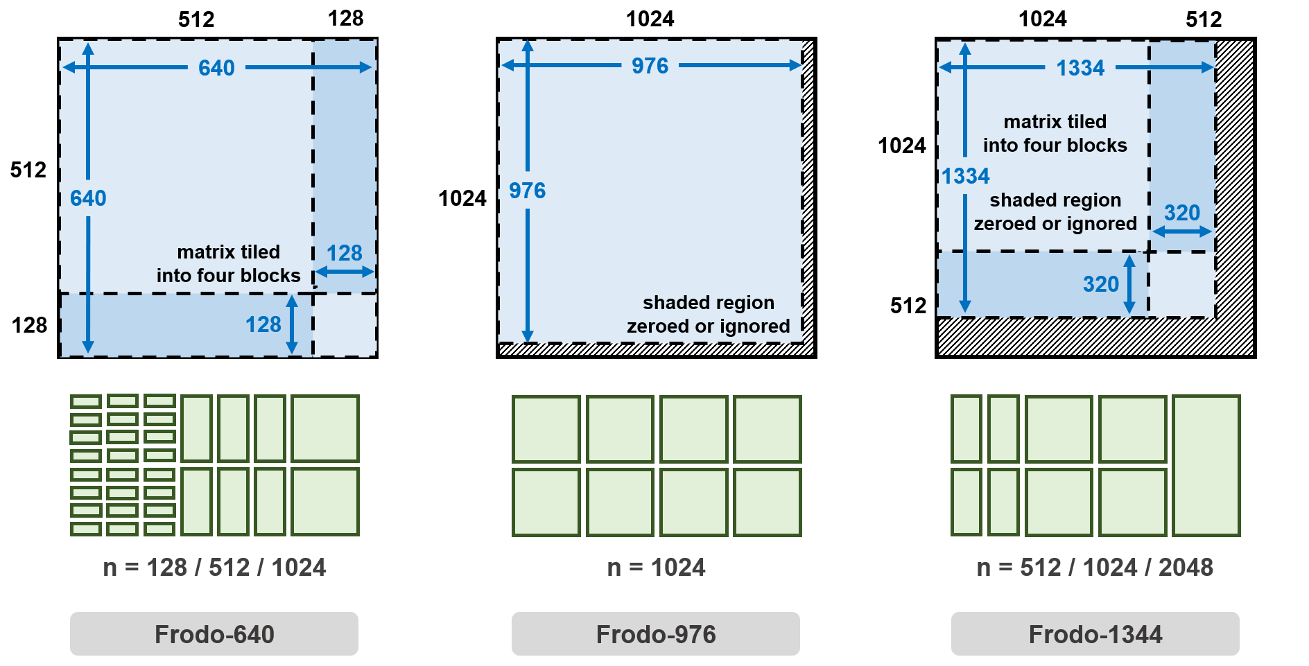
Frodo involves three large matrix multiplications: AS, S′A and S′B, where A, S, S′ and B have dimensions , , and respectively with and . We ensure that S′ is stored in row-major form and B is stored in column-major form, which simplifies calculating S′B using the schoolbook matrix multiplication technique. The poly_op instruction is used to coefficient-wise multiply a row of the multiplier matrix with a column of the multiplicand matrix, and the sum_elems instruction computes the sum of its elements to generate one element of the output matrix (please refer to Appendix B for details of our custom instructions). For calculating the matrix AS, we generate A in row-major form (using rejection sampling, with zero chance of rejection since is a power of two) and S in column major form (using CDT-based discrete Gaussian sampling) so that the same techniques still work. For , the matrix S is generated two columns at a time to reduce the number of outer loop iterations, as illustrated in the pseudo-code below:
#if (n == 1344)
for (j = 0; j < nbar; j = j + 1) {
#else
for (j = 0; j < nbar/2; j = j + 2) {
#endif
cdt_sample (prng = SHAKE-256, seed = r1, ..., poly = 0)
#if (n != 1344)
cdt_sample (prng = SHAKE-256, seed = r1, ..., poly = 1)
#endif
for (i = 0; i < n; i = i + 1) {
rej_sample (prng = SHAKE-128, seed = r0, ..., poly = 4)
#if (n != 1344)
poly_copy (poly_dst = 5, poly_src = 4)
#endif
poly_op (op = MUL, poly_dst = 4, poly_src = 0)
AS[i][j] = sum_elems (poly = 4)
#if (n != 1344)
poly_op (op = MUL, poly_dst = 5, poly_src = 1)
AS[i][j+1] = sum_elems (poly = 5)
#endif
}
}
Since both matrices S′ and A are generated on-the-fly in row-major fashion, this makes calculating S′A a bit complicated. We multiply each element of the i-th row of A with the i-th element of the j-th row of S′ to generate a partial sum. These i partial sums are incrementally added together to compute the j-th row of the output matrix S′A. Once again, we generate S two columns at a time to reduce the number of outer loop iterations. The corresponding pseudo-code is shown below:
#if (n == 1344)
for (j = 0; j < nbar; j = j + 1) {
#else
for (j = 0; j < nbar/2; j = j + 2) {
#endif
cdt_sample (prng = SHAKE-256, seed = r1, ..., poly = 0)
init (poly = 6)
#if (n != 1344)
cdt_sample (prng = SHAKE-256, seed = r1, ..., poly = 1)
init (poly = 7)
#endif
for (i = 0; i < n; i = i + 1) {
rej_sample (prng = SHAKE-128, seed = r0, ..., poly = 4)
reg = (poly = 0)[i]
poly_op (op = CONST_MUL, poly_dst = 2, poly_src = 4)
poly_op (op = ADD, poly_dst = 6, poly_src = 2)
#if (n != 1344)
reg = (poly = 1)[i]
poly_op (op = CONST_MUL, poly_dst = 3, poly_src = 4)
poly_op (op = ADD, poly_dst = 7, poly_src = 3)
#endif
}
}
where the reg = (poly)[i] instruction is used to save the i-th element of the array in the 24-bit internal register reg, the init (poly) instruction creates an array of zeros and the CONST_MUL operation multiplies each element of an array with the value stored in reg (please refer to Appendix B for details of our instructions). The AS + E and S′A + E′ computations require 10.9M and 9.9M cycles respectively for Frodo-640, and 25.3M and 23.2M cycles respectively for Frodo-976, and 67.1M and 62.7M cycles respectively for Frodo-1344, which constitute majority of the total cycle count. This is quite different from the Ring-LWE and Module-LWE schemes, where polynomial sampling accounts for 60-70% of the total computation cost. Please note that memory usage of Frodo-1344-CCA-KEM-Decaps exceeds the 64 KB processor data memory on our test chip; hence it was evaluated only in simulation, with power consumption extrapolated from measured power for Frodo-640 and Frodo-976.
In Tables 8 and 9, we have compared cycle count and energy consumption of assembly-optimized Cortex-M4 software [44] with our hardware-accelerated implementation on our test chip operating at 1.1 V and 72 MHz, with average cycle counts for 100 executions. Clearly, our design achieves up to an order of magnitude improvement in energy-efficiency and performance compared to state-of-the-art software. We note that Module-LWE schemes, although a bit slower compared to Ring-LWE, offer parameters with better scalability in terms of security and efficiency compared to Ring-LWE schemes. Among the key encapsulation schemes, NewHope and CRYSTALS-Kyber are two orders of magnitude more efficient than Frodo, owing to the inherent structure in ideal and module lattices where the key operation is polynomial multiplication as opposed to matrix multiplication in standard lattices. Among the digital signature schemes evaluated, qTESLA allows faster signature generation and verification compared to CRYSTALS-Kyber. However, our implementation of the key generation step in qTESLA is quite expensive since it uses CDT-based discrete Gaussian sampling with large tables and high precision. This is not a big concern since signature key-pairs are generated infrequently; also, more specialized hardware can be added to our architecture to support such distribution parameters, albeit at the cost of logic area.
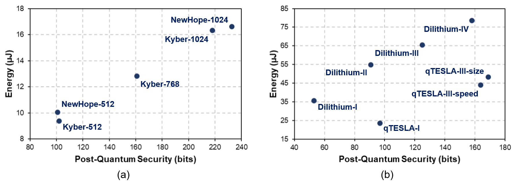
In Fig. 15, we plot the measured energy consumption of the Ring-LWE and Module-LWE-based CCA-KEM-Encaps and Sign algorithms at different post-quantum security levels, as implemented on our test chip operating at at 1.1 V and 72 MHz. Due to the configurability of our lattice crypto-processor, we are able to implement all these different modes and achieve energy scalability through efficiency versus security trade-offs.
| Protocol | Cortex-M4 [44] | This work | |||
|---|---|---|---|---|---|
| Cycles | Energy | Cycles | Power | Energy | |
| (J) | (mW) | (J) | |||
| NewHope-512-CCA-KEM | |||||
| KeyGen | - | - | 52,063 | 6.04 | 4.37 |
| Encaps | - | - | 136,077 | 5.30 | 10.02 |
| Decaps | - | - | 142,295 | 5.80 | 11.46 |
| NewHope-1024-CCA-KEM | |||||
| KeyGen | 1,243,729 | 764.89 | 97,969 | 6.13 | 8.35 |
| Encaps | 1,963,184 | 1207.34 | 236,812 | 5.05 | 16.59 |
| Decaps | 1,978,982 | 1217.07 | 258,872 | 5.89 | 21.17 |
| CRYSTALS-Kyber-512-CCA-KEM | |||||
| KeyGen | 726,921 | 447.06 | 74,519 | 5.77 | 5.97 |
| Encaps | 987,864 | 607.54 | 131,698 | 5.12 | 9.37 |
| Decaps | 1,018,946 | 626.65 | 142,309 | 5.69 | 11.25 |
| CRYSTALS-Kyber-768-CCA-KEM | |||||
| KeyGen | 1,200,291 | 738.18 | 111,525 | 5.28 | 8.19 |
| Encaps | 1,446,284 | 889.46 | 177,540 | 5.19 | 12.80 |
| Decaps | 1,477,365 | 908.58 | 190,579 | 5.86 | 15.52 |
| CRYSTALS-Kyber-1024-CCA-KEM | |||||
| KeyGen | 1,771,729 | 1089.61 | 148,547 | 5.95 | 12.27 |
| Encaps | 2,142,912 | 1317.89 | 223,469 | 5.25 | 16.3 |
| Decaps | 2,188,917 | 1346.18 | 240,977 | 5.91 | 19.76 |
| Frodo-640-CCA-KEM | |||||
| KeyGen | 81,293,476 | 49995.49 | 11,453,942 | 6.65 | 1057.65 |
| Encaps | 86,178,252 | 52999.62 | 11,609,668 | 7.01 | 1129.95 |
| Decaps | 87,170,982 | 53610.15 | 12,035,513 | 6.88 | 1150.83 |
| Frodo-976-CCA-KEM | |||||
| KeyGen | - | - | 26,005,326 | 6.70 | 2420.97 |
| Encaps | - | - | 29,749,417 | 7.05 | 2912.95 |
| Decaps | - | - | 30,421,175 | 6.94 | 2932.13 |
| Frodo-1344-CCA-KEM | |||||
| KeyGen | - | - | 67,994,170 | 6.75 | 6374.45 |
| Encaps | - | - | 71,501,358 | 7.10 | 7050.83 |
| Decaps | - | - | 72,526,695 | 7.00 | 7051.21 |
| Protocol | Cortex-M4 [44] | This work | |||
|---|---|---|---|---|---|
| Cycles | Energy | Cycles | Power | Energy | |
| (J) | (mW) | (J) | |||
| qTESLA-I | |||||
| KeyGen | 17,545,901 | 10790.73 | 4,846,949 | 7.89 | 531.55 |
| Sign | 6,317,445 | 3885.23 | 168,273 | 9.99 | 23.34 |
| Verify | 1,059,370 | 651.51 | 38,922 | 7.99 | 4.32 |
| qTESLA-III-size | |||||
| KeyGen | 58,227,852 | 35810.13 | 11,479,190 | 7.71 | 1229.18 |
| Sign | 19,869,370 | 12219.66 | 348,429 | 9.97 | 48.23 |
| Verify | 2,297,530 | 1412.98 | 69,154 | 7.59 | 7.27 |
| qTESLA-III-speed | |||||
| KeyGen | 30,720,411 | 18893.05 | 11,898,241 | 7.64 | 1262.39 |
| Sign | 11,987,079 | 7372.05 | 317,083 | 9.97 | 43.91 |
| Verify | 2,225,296 | 1368.56 | 67,712 | 7.30 | 6.86 |
| CRYSTALS-Dilithium-I | |||||
| KeyGen | - | - | 95,202 | 6.82 | 9.00 |
| Sign | - | - | 376,392 | 6.77 | 35.41 |
| Verify | - | - | 142,576 | 7.73 | 15.31 |
| CRYSTALS-Dilithium-II | |||||
| KeyGen | - | - | 130,022 | 7.24 | 13.08 |
| Sign | - | - | 514,246 | 7.68 | 54.82 |
| Verify | - | - | 184,933 | 7.49 | 19.23 |
| CRYSTALS-Dilithium-III | |||||
| KeyGen | 2,322,955 | 1428.62 | 167,433 | 7.36 | 17.11 |
| Sign | 9,978,000 | 6136.47 | 634,763 | 7.40 | 65.26 |
| Verify | 2,322,765 | 1428.50 | 229,481 | 7.41 | 23.63 |
| CRYSTALS-Dilithium-IV | |||||
| KeyGen | - | - | 223,272 | 6.89 | 21.38 |
| Sign | - | - | 815,636 | 6.93 | 78.53 |
| Verify | - | - | 276,221 | 7.44 | 28.55 |
In Table 10, we compare our design with existing hardware-accelerated implementations of NIST Round 2 lattice-based protocols. Our crypto-processor is significantly smaller than the multiple designs generated using high-level synthesis in [20], and is also more flexible and energy-efficient. Our Kyber implementation is faster than [18] which uses RSA, AES and SHA hardware accelerators on the SLE 78 security controller platform to accelerate lattice cryptography. Efficiency of our design is greater than or comparable to state-of-the-art FPGA implementations of Ring-LWE [13, 60]. Notably, [60] also uses a RISC-V processor with NTT and SHA accelerators to implement the NewHope protocol. However, our implementation of Frodo, which re-purposes the Ring/Module-LWE hardware for LWE computations, is not as efficient as the dedicated LWE accelerator in [16]. Finally, we also compare our design with state-of-the-art pre-quantum elliptic curve cryptography hardware [56, 61], and we observe our implementation of CCA-secure lattice-based key encapsulation using NewHope-512 to be around more efficient compared to elliptic curve Diffie-Hellman key exchange using the NIST P-256 curve at comparable pre-quantum security level.
| Design | Platform | Tech | VDD | Freq | Protocol | Area | Cycles | Energy |
| (nm) | (V) | (MHz) | (kGE) | (J) | ||||
| This work | ASIC | 40 | 1.1 | 72 | NewHope-512-CCA-KEM-Encaps | 106 | 136,077 | 10.02 |
| NewHope-1024-CPA-PKE-Encrypt | 106,611 | 12.00 | ||||||
| Kyber-512-CCA-KEM-Encaps | 131,698 | 9.37 | ||||||
| Kyber-768-CPA-PKE-Encrypt | 94,440 | 10.31 | ||||||
| Kyber-768-CCA-KEM-Encaps | 177,540 | 12.80 | ||||||
| Frodo-640-CCA-KEM-Encaps | 11,609,668 | 1129.95 | ||||||
| Dilithium-II-Sign | 514,246 | 54.82 | ||||||
| Basu et al. [20] | ASIC | 65 | 1.2 | 169 | NewHope-512-CCA-KEM-Encaps | 1273 | 307,847 | 69.42 |
| 200 | Kyber-512-CCA-KEM-Encaps | 1341 | 31,669 | 6.21 | ||||
| 158 | Dilithium-II-Sign | 1603 | 155,166 | 50.42 | ||||
| Albrecht et al. [18] | SLE 78 | - | - | 50 | Kyber-768-CPA-PKE-Encrypt | - | 4,747,291 | - |
| Kyber-768-CCA-KEM-Encaps | 5,117,996 | |||||||
| Oder et al. [13] | FPGA | - | - | 117 | NewHope-1024-Simple-Encrypt | - | 179,292 | - |
| Howe et al. [16] | FPGA | - | - | 167 | Frodo-640-CCA-KEM-Encaps | - | 3,317,760 | - |
| Fritzmann et al. [60] | FPGA | - | - | - | NewHope-1024-CPA-PKE-Encrypt | - | 589,285 | - |
| Hutter et al. [61] | ASIC | 130 | 1.2 | 1 | Curve25519-ECDHE | 50 | 1,622,354 | 113.56 |
| Banerjee et al. [56] | ASIC | 65 | 1.2 | 20 | NIST-P256-ECDHE | 149 | 680,000 | 24.07 |
| NIST-P256-ECDSA-Sign | 180,000 | 6.48 | ||||||
| Only post-synthesis area and energy consumption reported | ||||||||
6.2 Side-Channel Analysis
Side-channel security is an important aspect of all public-key cryptography implementations and lattice-based cryptography is not an exception. In order to prevent information leakage through timing side channels, the most important requirement is to ensure that the timing and memory access patterns of underlying computations are independent of the secret data being computed upon. In our implementation, this is achieved either by making the computations constant-time, e.g., binomial sampling, discrete Gaussian sampling, NTT and polynomial arithmetic, or by using rejection sampling, e.g, sampling numbers from or or probabilistic rejection during signature schemes. Since our cryptographic core and RISC-V processor both have a single-level memory hierarchy, the possibility of cache timing attacks is also eliminated.
Our power side-channel measurement setup is shown in Fig. 17. Our test board has an 18 resistor connected in series between the power supply and the VDD pin of our test chip. The voltage across this resistor, proportional to the chip’s current draw, is magnified using a non-inverting differential amplifier (consists of an AD8001 op-amp chip, with 6 dB flat gain up to 100 MHz, in the non-inverting configuration with resistors of appropriate sizes) and then observed through a 2.5 GS/s Tektronix MDO3024 mixed domain oscilloscope.
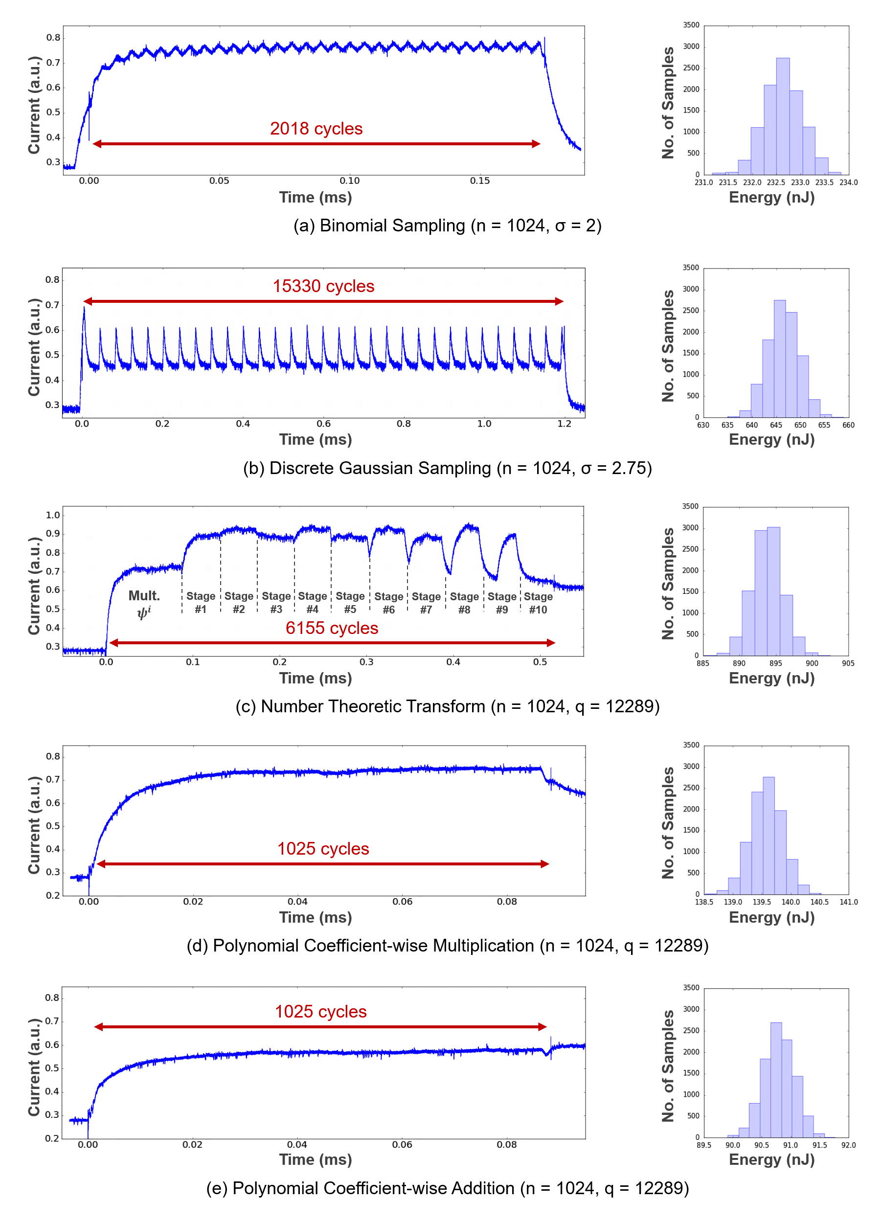
The execution times of binomial sampling, discrete Gaussian sampling, NTT, polynomial coefficient-wise multiplication and addition (with and ) were measured for 10,000 random executions to verify that these computations are indeed constant-time. The corresponding power waveforms and energy consumption histograms, measured from our test chip operating at 1.1 V and 12 MHz, are shown in Fig. 16.
Typical simple power analysis (SPA) attacks on lattice cryptography implementations exploit information leakage through conditional branching or data-dependent execution times during the modular arithmetic computations in NTT or polynomial coefficient-wise multiplication [62, 63, 64]. As explained in Fig. 16, our implementation of polynomial arithmetic is constant-time. To quantitatively evaluate SPA resistance of our design, we perform a difference-of-means test [65, 64, 66] on three polynomial operations – NTT, coefficient-wise multiplication and coefficient-wise addition – which are traditionally used as attack points. In this test, we try to differentiate two sets of measurements – those with a particular coefficient (‘0’-th coefficient in our case) in the input polynomial set to 0 (denoted as set ‘0’ or ) versus the same coefficient set to (denoted as set ‘1’ or ) – by comparing their means separately for each point in the mean power trace. The difference-of-means is calculated for increasing number of measurements and plotted as a function of the number of traces . The corresponding 99.99% confidence interval for having a zero difference of means between these two sets is calculated as , where and are the standard deviations of the two sets and respectively and is the critical -statistic for degrees of freedom and cumulative probability . As long as the absolute difference-of-means is smaller than the confidence interval, it is a strong indicator that the sets and are indistinguishable.
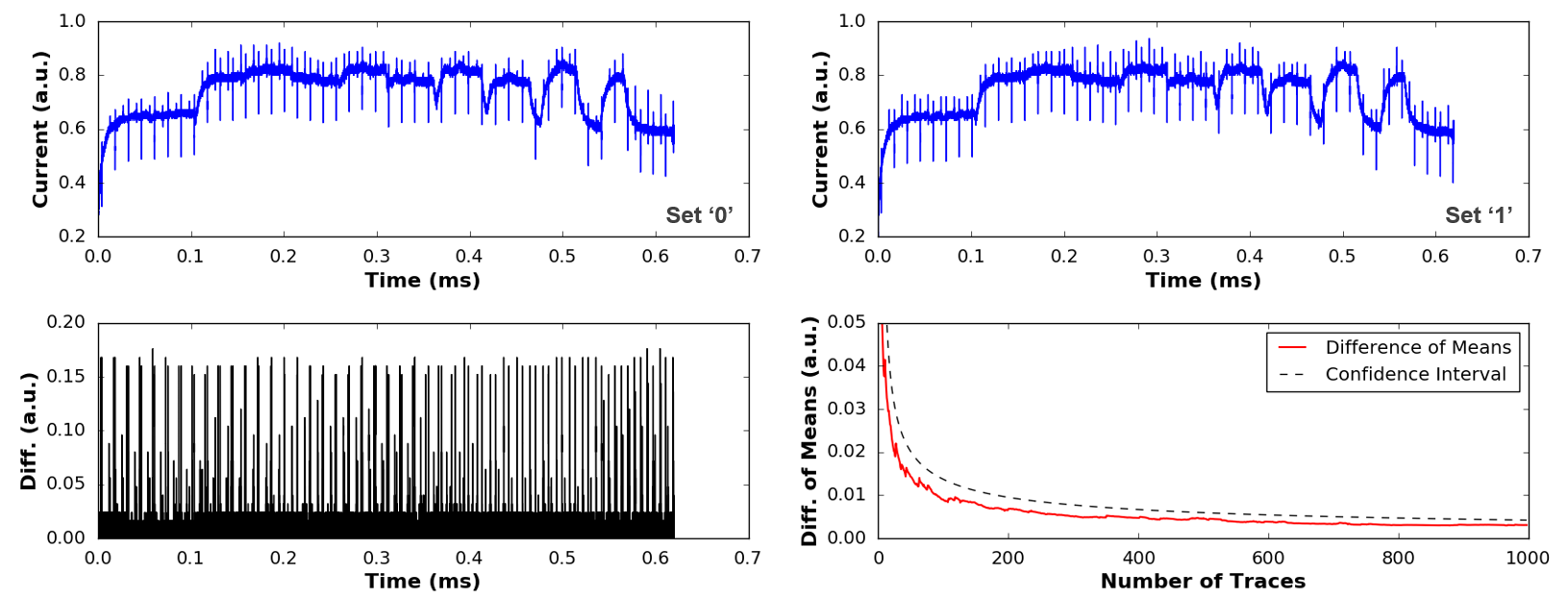
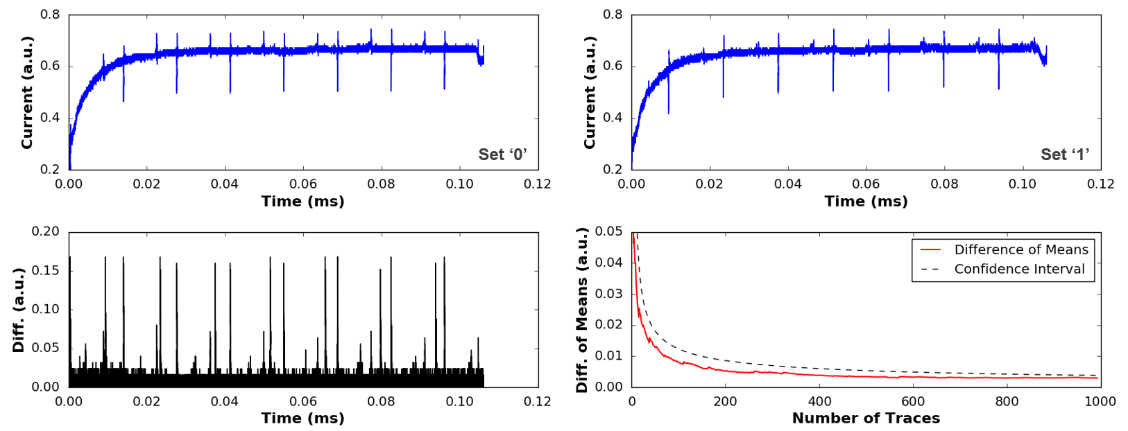
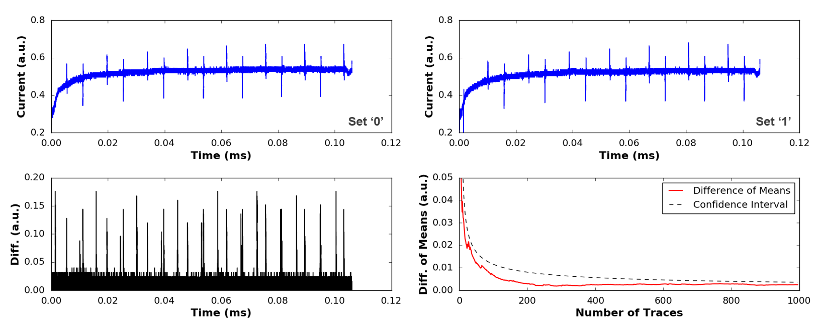
In Figures 18, 19 and 20, we provide preliminary difference-of-means test results for three polynomial operations (with and ) as measured from our test chip operating at 1.1 V and 10 MHz. Sampling rate of the oscilloscope was set to 500 MS/s for NTT and 2.5 GS/s for coefficient-wise multiplication and addition. The red lines denote measured difference-of-means, and the dashed lines mark the 99.99% confidence interval for ideal zero difference-of-means. These results validate that our design is secure against SPA side-channel attacks.
The protocol implementations discussed earlier do not have any explicit countermeasures against differential power analysis (DPA) attacks. Although DPA attacks can be mitigated by using ephemeral keys, it is still important to analyze how these protocols can be made DPA-secure. Masking-based countermeasures have been proposed in [67, 68, 46] for Ring-LWE encryption. Since our crypto-processor is programmable, such masked protocols can be implemented using the right mix of software and hardware acceleration. For example, we consider NewHope-CPA-PKE and discuss how the masked decryption algorithm, inspired by [67, 68, 46], can be implemented using our hardware. A simplified version of the CPA-PKE scheme, excluding any key / ciphertext compression / decompression and encoding / decoding and implementation-specific details, is provided below:
function NewHope-CPA-PKE.KeyGen():
Sample
return (, )
function NewHope-CPA-PKE.Encrypt():
Sample
Encode
return
function NewHope-CPA-PKE.Decrypt():
Decode
return
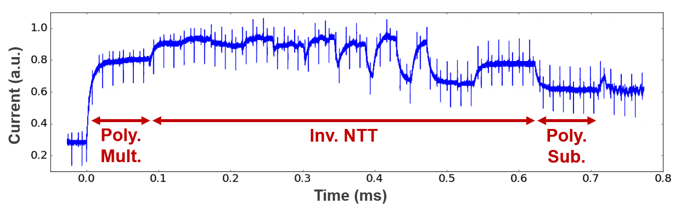
where is the 32-byte message to be encrypted, is the NTT representation of polynomial , denotes coefficient-wise multiplication (in the transform domain) and denotes polynomial multiplication in . The Encode function converts message into a polynomial in . To allow robustness against errors, each bit of the 256-bit message is encoded into coefficients. For example, for , the -th, -th, -th and -th coefficients are set to 0 or depending on whether the -th bit in is 0 or 1 respectively, for . The Decode function maps coefficients of a polynomial back to the original message bit. For example, for , it takes the -th, -th, -th and -th coefficients (each in the range , subtracts from each of them, accumulates their absolute values, and finally sets the -th message bit to 0 if the sum is larger than or to 1 otherwise, for . Further details about these functions are available in the NewHope specification document [24]. The Decrypt algorithm requires one polynomial coefficient-wise multiplication , one inverse NTT (including multiplication with ) to compute , and one polynomial coefficient-wise subtraction . Figure 21 shows the corresponding measured power waveform for .
Similar to the encryption scheme studied in [68], we note that NewHope-CPA-PKE is also additively homomorphic, that is, if and are the ciphertexts corresponding to messages and respectively, under the same key-pair, then will be the ciphertext corresponding to . Following the works of [67, 68, 46], this property can be exploited to randomize the decryption algorithm (as a first-order DPA countermeasure) as explained below:
-
1.
Generate a secret random message
-
2.
Encrypt to its corresponding ciphertext
-
3.
Compute , where is the original ciphertext
-
4.
Decrypt masked ciphertext to obtain , where is the original message
-
5.
Recover original message
Therefore, the masked decryption now requires generation of a random message along with invocations of both the Encrypt and Decrypt functions. As explained earlier, these functions can be implemented entirely using Sapphire custom programs, so the masking involves minimal software overheads. Referring to the cycle counts and energy consumption of NewHope-1024-CPA-PKE in Table 7, we note that the masked decryption is about less efficient compared to the unmasked version, both in terms of energy and performance. Since is independent from the original message , the ciphertext can be pre-computed offline in order to reduce online computation time and energy consumption. As explained in [68], this technique does not require any modifications to the Decode function. However, addition of ciphertexts increases the noise in them, thus increasing the decryption failure rate. Each of the two polynomials in the ciphertext contains one noise term whose coefficients are derived from the zero-mean binomial distribution with support and standard deviation ( for NewHope). When two such ciphertexts are added, the resulting noise distribution (still binomial) now has support with standard deviation , that is, the noise variance is doubled. For , which is also used in NewHope-Simple, the decryption failure probability will go up from [24] to [69]. As discussed in [68], standard deviation of the error distribution can be decreased to allow correct decryptions at the cost of a minor deterioration in security. So, one possibility is to set in the unmasked scheme (so that for masked decryption and failure probability remains ). The corresponding decrease in security level is from 289 bits to 268 bits, as obtained from the LWE hardness estimator [70] using the following Sage module:
load("https://bitbucket.org/malb/lwe-estimator/raw/HEAD/estimator.py")
n = 1024; q = 12289; stddev = sqrt(4/2); alpha = sqrt(2*pi)*stddev/q
_ = estimate_lwe(n, alpha, q, reduction_cost_model=BKZ.sieve)
7 Conclusion and Future Work
In this work, we have presented a configurable lattice cryptography processor supporting different parameters for NIST Round 2 lattice-based key encapsulation and digital signature protocols such as NewHope, qTESLA, CRYSTALS-Kyber, CRYSTALS-Dilithium and Frodo. Efficient modular arithmetic, sampling and NTT memory architectures together provide an order of magnitude improvement in performance and energy-efficiency compared to state-of-the-art software and hardware implementations. Our ASIC implementation was fabricated in a 40nm low-power CMOS process and all measurement results are obtained from our test chip operating at 1.1 V and 72 MHz. Our protocol implementations are secure against timing and simple power analysis attacks, and we also discuss how masking countermeasures against differential power analysis can be implemented using the programmability of our crypto-processor.
Since our design supports configurable lattice parameters, it will be interesting to explore other lattice-based protocols such as Saber [71] and Round5 [72], which are based on the LWR (learning with rounding) problem [73]. More concrete analysis of DPA-secure masked implementations, for CPA-PKE, CCA-KEM and signature schemes, along with leakage tests and impact on performance and energy-efficiency, will also be performed in the future. Finally, non-lattice-based post-quantum protocols can also be implemented on our platform, using a mix of hardware acceleration and software, since they can still benefit from our efficient implementation of modular arithmetic and SHA-3 computations.
Acknowledgements
The authors would like to thank Texas Instruments for funding this work, the TSMC University Shuttle Program for chip fabrication support, and Bluespec, Xilinx, Cadence, Synopsys and Mentor Graphics for providing CAD tools. The authors also thank the anonymous reviewers for their valuable comments and suggestions.
References
- [1] P. W. Shor, “Polynomial-Time Algorithms for Prime Factorization and Discrete Logarithms on a Quantum Computer,” SIAM Journal of Computing, vol. 26, pp. 1484–1509, Oct. 1997.
- [2] L. Chen, S. Jordan, Y. Liu, D. Moody, R. Peralta, R. Perlner, and D. Smith-Tone, “Report on Post-Quantum Cryptography,” Tech. Rep. 8105, National Institute of Standards and Technology, Apr. 2016.
- [3] G. Alagic, J. Alperin-Sheriff, D. Apon, D. Cooper, Q. Dang, C. Miller, D. Moody, R. Peralta, R. Perlner, A. Robinson, D. Smith-Tone, and Y. Liu, “Status Report on the First Round of the NIST Post-Quantum Cryptography Standardization Process,” Tech. Rep. 8240, National Institute of Standards and Technology, Jan. 2019.
- [4] O. Regev, “On Lattices, Learning with Errors, Random Linear Codes, and Cryptography,” in Proceedings of the Thirty-Seventh Annual ACM Symposium on Theory of Computing (STOC), pp. 84–93, May 2005.
- [5] V. Lyubashevsky, C. Peikert, and O. Regev, “On Ideal Lattices and Learning with Errors over Rings,” Journal of the ACM, vol. 60, pp. 43:1–43:35, Nov. 2013.
- [6] A. Langlois and D. Stehle, “Worst-case to Average-case Reductions for Module Lattices,” Designs, Codes and Cryptography, vol. 75, pp. 565–599, Jun. 2015.
- [7] Z. Brakerski, A. Langlois, C. Peikert, O. Regev, and D. Stehle, “Classical Hardness of Learning with Errors,” in Proceedings of the Forty-fifth Annual ACM Symposium on Theory of Computing (STOC), pp. 575–584, Jun. 2013.
- [8] O. Regev, “Quantum Computation and Lattice Problems,” SIAM Journal of Computing, vol. 33, pp. 738–760, Mar. 2004.
- [9] S. S. Roy, F. Vercauteren, N. Mentens, D. D. Chen, and I. Verbauwhede, “Compact Ring-LWE Cryptoprocessor,” in Cryptographic Hardware and Embedded Systems – CHES 2014, pp. 371–391, Sep. 2014.
- [10] R. de Clercq, S. S. Roy, F. Vercauteren, and I. Verbauwhede, “Efficient Software Implementation of Ring-LWE Encryption,” in 2015 Design, Automation Test in Europe Conference Exhibition (DATE), pp. 339–344, Mar. 2015.
- [11] E. Alkim, P. Jakubeit, and P. Schwabe, “NewHope on ARM Cortex-M,” in Security, Privacy, and Applied Cryptography Engineering – SPACE 2016, pp. 332–349, Dec. 2016.
- [12] P.-C. Kuo, W.-D. Li, Y.-W. Chen, Y.-C. Hsu, B.-Y. Peng, C.-M. Cheng, and B.-Y. Yang, “High Performance Post-Quantum Key Exchange on FPGAs.” Cryptology ePrint Archive, Report 2017/690, 2017. https://eprint.iacr.org/2017/690.
- [13] T. Oder and T. Guneysu, “Implementing the NewHope-Simple Key Exchange on low-cost FPGAs,” in International Conference on Cryptology and Information Security in Latin America, – LATINCRYPT 2017, pp. 371–391, Sep. 2017.
- [14] H. Nejatollahi, N. Dutt, I. Banerjee, and R. Cammarota, “Domain-specific Accelerators for Ideal Lattice-based Public Key Protocols.” Cryptology ePrint Archive, Report 2018/608, 2018. https://eprint.iacr.org/2018/608.
- [15] J. W. Bos, S. Friedberger, M. Martinoli, E. Oswald, and M. Stam, “Fly, you fool! Faster Frodo for the ARM Cortex-M4.” Cryptology ePrint Archive, Report 2018/1116, 2018. https://eprint.iacr.org/2018/1116.
- [16] J. Howe, T. Oder, M. Krausz, and T. Guneysu, “Standard Lattice-Based Key Encapsulation on Embedded Devices,” IACR Transactions on Cryptographic Hardware and Embedded Systems, vol. 2018, pp. 372–393, Aug. 2018.
- [17] S. Song, W. Tang, T. Chen, and Z. Zhang, “LEIA: A 2.05mm2 140mW Lattice Encryption Instruction Accelerator in 40nm CMOS,” in 2018 IEEE Custom Integrated Circuits Conference (CICC), pp. 1–4, Apr. 2018.
- [18] M. Albrecht, C. Hanser, A. Holler, T. Poppelmann, F. Virdia, and A. Wallner, “Implementing RLWE-based Schemes Using an RSA Co-Processor,” IACR Transactions on Cryptographic Hardware and Embedded Systems, vol. 2019, pp. 169–208, Nov. 2018.
- [19] D. Liu, C. Zhang, H. Lin, Y. Chen, and M. Zhang, “A Resource-Efficient and Side-Channel Secure Hardware Implementation of Ring-LWE Cryptographic Processor,” IEEE Transactions on Circuits and Systems I: Regular Papers, vol. 66, pp. 1474–1483, Apr. 2019.
- [20] K. Basu, D. Soni, M. Nabeel, and R. Karri, “NIST Post-Quantum Cryptography - A Hardware Evaluation Study.” Cryptology ePrint Archive, Report 2019/047, 2019. https://eprint.iacr.org/2019/047.
- [21] H. Nejatollahi, N. Dutt, S. Ray, F. Regazzoni, I. Banerjee, and R. Cammarota, “Post-Quantum Lattice-Based Cryptography Implementations: A Survey,” ACM Computing Surveys, vol. 51, pp. 129:1–129:41, Jan. 2019.
- [22] T. Oder, T. Guneysu, F. Valencia, A. Khalid, M. O’Neill, and F. Regazzoni, “Lattice-based Cryptography: From Reconfigurable Hardware to ASIC,” in 2016 International Symposium on Integrated Circuits (ISIC), pp. 1–4, Dec. 2016.
- [23] M. Naehrig, E. Alkim, J. Bos, L. Ducas, K. Easterbrook, B. LaMacchia, P. Longa, I. Mironov, V. Nikolaenko, C. Peikert, A. Raghunathan, and D. Stebila, “FrodoKEM: Learning With Errors Key Encapsulation – Algorithm Specifications And Supporting Documentation,” tech. rep., National Institute of Standards and Technology, 2019. https://csrc.nist.gov/Projects/Post-Quantum-Cryptography/Round-2-Submissions.
- [24] T. Poppelmann, E. Alkim, R. Avanzi, J. Bos, L. Ducas, A. de la Piedra, P. Schwabe, D. Stebila, M. R. Albrecht, E. Orsini, V. Osheter, K. G. Paterson, G. Peer, and N. P. Smart, “NewHope – Algorithm Specifications And Supporting Documentation,” tech. rep., National Institute of Standards and Technology, 2019. https://csrc.nist.gov/Projects/Post-Quantum-Cryptography/Round-2-Submissions.
- [25] N. Bindel, S. Akleylek, E. Alkim, P. S. L. M. Barreto, J. Buchmann, E. Eaton, G. Gutoski, J. Kramer, P. Longa, H. Polat, J. E. Ricardini, and G. Zanon, “Lattice-based Digital Signature Scheme qTESLA – Submission to NIST’s Post-Quantum Project,” tech. rep., National Institute of Standards and Technology, 2019. https://csrc.nist.gov/Projects/Post-Quantum-Cryptography/Round-2-Submissions.
- [26] P. Schwabe, R. Avanzi, J. Bos, L. Ducas, E. Kiltz, T. Lepoint, V. Lyubashevsky, J. M. Schanck, G. Seiler, and D. Stehle, “CRYSTALS-Kyber – Algorithm Specifications And Supporting Documentation,” tech. rep., National Institute of Standards and Technology, 2019. https://csrc.nist.gov/Projects/Post-Quantum-Cryptography/Round-2-Submissions.
- [27] V. Lyubashevsky, L. Ducas, E. Kiltz, T. Lepoint, P. Schwabe, G. Seiler, and D. Stehle, “CRYSTALS-Dilithium – Algorithm Specifications And Supporting Documentation,” tech. rep., National Institute of Standards and Technology, 2019. https://csrc.nist.gov/Projects/Post-Quantum-Cryptography/Round-2-Submissions.
- [28] D. J. Bernstein, “Fast Multiplication and its Applications,” Algorithmic Number Theory, vol. 44, pp. 325–384, 2008.
- [29] T. H. Cormen, C. E. Leiserson, R. L. Rivest, and C. Stein, Introduction to Algorithms. The MIT Press, 3rd ed., 2009.
- [30] C. Du and G. Bai, “Towards Efficient Polynomial Multiplication for Lattice-based Cryptography,” in 2016 IEEE International Symposium on Circuits and Systems (ISCAS), pp. 1178–1181, May 2016.
- [31] R. R. Howell, Algorithms: A Top-Down Approach. Draft, 2012. http://people.cs.ksu.edu/~rhowell/algorithms-text.
- [32] P. Longa and M. Naehrig, “Speeding up the Number Theoretic Transform for Faster Ideal Lattice-Based Cryptography.” Cryptology ePrint Archive, Report 2016/504, 2016. https://eprint.iacr.org/2016/504.
- [33] P. Barrett, “Implementing the Rivest Shamir and Adleman Public Key Encryption Algorithm on a Standard Digital Signal Processor,” in Advances in Cryptology – CRYPTO 86, pp. 311–323, Aug. 1986.
- [34] M. Seo, J. H. Park, D. H. Lee, S. Kim, and S.-J. Lee, “EMBLEM and R.EMBLEM – Error-blocked Multi-Bit LWE-based Encapsulation Mechanism,” tech. rep., National Institute of Standards and Technology, 2017. https://csrc.nist.gov/Projects/Post-Quantum-Cryptography/Round-1-Submissions.
- [35] C. Chen, J. Hoffstein, W. Whyte, and Z. Zhang, “NIST PQ Submission: pqNTRUSign – A Modular Lattice Signature Scheme,” tech. rep., National Institute of Standards and Technology, 2017. https://csrc.nist.gov/Projects/Post-Quantum-Cryptography/Round-1-Submissions.
- [36] J. Ding, T. Takagi, X. Gao, and Y. Wang, “Ding Key Exchange,” tech. rep., National Institute of Standards and Technology, 2017. https://csrc.nist.gov/Projects/Post-Quantum-Cryptography/Round-1-Submissions.
- [37] M. R. Albrecht, Y. Lindell, E. Orsini, V. Osheter, K. G. Paterson, G. Peer, and N. P. Smart, “LIMA –- A PQC Encryption Scheme,” tech. rep., National Institute of Standards and Technology, 2017. https://csrc.nist.gov/Projects/Post-Quantum-Cryptography/Round-1-Submissions.
- [38] U. Banerjee, A. Pathak, and A. P. Chandrakasan, “An Energy-Efficient Configurable Lattice Cryptography Processor for the Quantum-Secure Internet of Things,” in 2019 IEEE International Solid-State Circuits Conference (ISSCC), pp. 46–48, Feb. 2019.
- [39] D. D. Chen, N. Mentens, F. Vercauteren, S. S. Roy, R. C. C. Cheung, D. Pao, and I. Verbauwhede, “High-Speed Polynomial Multiplication Architecture for Ring-LWE and SHE Cryptosystems,” IEEE Transactions on Circuits and Systems I: Regular Papers, vol. 62, pp. 157–166, Jan. 2015.
- [40] H. Noguchi, S. Okumura, Y. Iguchi, H. Fujiwara, Y. Morita, K. Nii, H. Kawaguchi, and M. Yoshimoto, “Which is the Best Dual-Port SRAM in 45-nm Process Technology? — 8T, 10T Single End, and 10T Differential —,” in 2008 IEEE International Conference on Integrated Circuit Design and Technology and Tutorial, pp. 55–58, Jun. 2008.
- [41] M. C. Pease, “An Adaptation of the Fast Fourier Transform for Parallel Processing,” Journal of the ACM, vol. 15, pp. 252–264, Apr. 1968.
- [42] J. M. Pollard, “The Fast Fourier Transform in a Finite Field,” Mathematics of Computation, vol. 25, pp. 365–374, May 1971.
- [43] T. Fritzmann and J. Sepúlveda, “Efficient and Flexible Low-Power NTT for Lattice-Based Cryptography,” in 2019 IEEE International Symposium on Hardware Oriented Security and Trust (HOST), pp. 141–150, May 2019.
- [44] M. J. Kannwischer, J. Rijneveld, P. Schwabe, and K. Stoffelen, “PQM4: Post-quantum crypto library for the ARM Cortex-M4,” 2018. https://github.com/mupq/pqm4.
- [45] STMicroelectronics, “NUCLEO-F411RE Development Board.” https://os.mbed.com/platforms/ST-Nucleo-F411RE.
- [46] T. Oder, T. Schneider, T. Poppelmann, and T. Guneysu, “Practical CCA2-Secure and Masked Ring-LWE Implementation,” IACR Transactions on Cryptographic Hardware and Embedded Systems, vol. 2018, pp. 142–174, Feb. 2018.
- [47] NIST, “SHA-3 Standard: Permutation-Based Hash and Extendable-Output Functions,” Tech. Rep. FIPS PUB 202, National Institute of Standards and Technology, Aug. 2015.
- [48] NIST, “Advanced Encryption Standard (AES),” Tech. Rep. FIPS PUB 197, National Institute of Standards and Technology, Nov. 2001.
- [49] D. J. Bernstein, “ChaCha, a variant of Salsa20,” Jan. 2008. https://cr.yp.to/chacha/chacha-20080128.pdf.
- [50] G. Bertoni, J. Daemen, M. Peeters, and G. Van Assche, “Keccak Specifications,” 2009.
- [51] S. Gueron and F. Schlieker, “Speeding up R-LWE Post-Quantum Key Exchange.” Cryptology ePrint Archive, Report 2016/467, 2016. https://eprint.iacr.org/2016/467.
- [52] D. E. Knuth and A. C. Yao, Algorithms and Complexity: New Directions and Recent Results, ch. The Complexity of Non-Uniform Random Number Generation. Academic Press, 1976.
- [53] J. Follath, “Gaussian Sampling in Lattice Based Cryptography,” Tatra Mountains Mathematical Publications, vol. 60, pp. 1–23, Sep. 2014.
- [54] J. H. Cheon, S. Park, J. Lee, D. Kim, Y. Song, S. Hong, D. Kim, J. Kim, S.-M. Hong, A. Yun, J. Kim, H. Park, E. Choi, K. Kim, J.-S. Kim, and J. Lee, “Lizard Public Key Encryption,” tech. rep., National Institute of Standards and Technology, 2017. https://csrc.nist.gov/Projects/Post-Quantum-Cryptography/Round-1-Submissions.
- [55] A. Karmakar, J. M. Bermudo Mera, S. S. Roy, and I. Verbauwhede, “Saber on ARM,” IACR Transactions on Cryptographic Hardware and Embedded Systems, vol. 2018, pp. 243–266, Aug. 2018.
- [56] U. Banerjee, C. Juvekar, A. Wright, Arvind, and A. P. Chandrakasan, “An Energy-Efficient Reconfigurable DTLS Cryptographic Engine for End-to-End Security in IoT Applications,” in 2018 IEEE International Solid-State Circuits Conference (ISSCC), pp. 42–44, Feb. 2018.
- [57] A. Waterman, Y. Lee, D. A. Patterson, and K. Asanovic, “The RISC-V Instruction Set Manual,” 2014.
- [58] M. Dichtl and J. D. Golic, “High-Speed True Random Number Generation with Logic Gates Only,” in Cryptographic Hardware and Embedded Systems - CHES 2007, pp. 45–62, Sep. 2007.
- [59] E. Fujisaki and T. Okamoto, Tatsuaki, “Secure Integration of Asymmetric and Symmetric Encryption Schemes,” Journal of Cryptology, vol. 26, pp. 80–101, Jan. 2013.
- [60] T. Fritzmann, U. Sharif, D. Müller-Gritschneder, C. Reinbrecht, U. Schlichtmann, and J. Sepulveda, “Towards Reliable and Secure Post-Quantum Co-Processors based on RISC-V,” in 2019 Design, Automation Test in Europe Conference Exhibition (DATE), pp. 1148–1153, Mar. 2019.
- [61] M. Hutter, J. Schilling, P. Schwabe, and W. Wieser, “Nacl’s crypto_box in hardware,” in Cryptographic Hardware and Embedded Systems – CHES 2015, pp. 81–101, Sep. 2015.
- [62] A. Park and D. Han, “Chosen Ciphertext Simple Power Analysis on Software 8-bit Implementation of Ring-LWE Encryption,” in 2016 IEEE Asian Hardware-Oriented Security and Trust (AsianHOST), pp. 1–6, Dec 2016.
- [63] R. Primas, P. Pessl, and S. Mangard, “Single-Trace Side-Channel Attacks on Masked Lattice-Based Encryption,” in Cryptographic Hardware and Embedded Systems – CHES 2017, pp. 513–533, Sep. 2017.
- [64] A. Aysu, M. Orshansky, and M. Tiwari, “Binary Ring-LWE Hardware with Power Side-Channel Countermeasures,” in 2018 Design, Automation Test in Europe Conference Exhibition (DATE), pp. 1253–1258, Mar. 2018.
- [65] P. Kocher, J. Jaffe, B. Jun, and P. Rohatgi, “Introduction to Differential Power Analysis,” Journal of Cryptographic Engineering, vol. 1, pp. 5–27, Apr. 2011.
- [66] S. Ebrahimi, S. Bayat-Sarmadi, and H. Mosanaei-Boorani, “Post-Quantum Cryptoprocessors Optimized for Edge and Resource-Constrained Devices in IoT,” IEEE Internet of Things Journal, vol. 6, pp. 5500–5507, Jun. 2019.
- [67] O. Reparaz, S. S. Roy, F. Vercauteren, and I. Verbauwhede, “A Masked Ring-LWE Implementation,” in Cryptographic Hardware and Embedded Systems – CHES 2015, pp. 683–702, Sep. 2015.
- [68] O. Reparaz, R. d. S. S. Roy, F. Vercauteren, and I. Verbauwhede, “Additively homomorphic ring-lwe masking,” in Post-Quantum Cryptography, pp. 233–244, Feb. 2016.
- [69] E. Alkim, L. Ducas, T. Poppelmann, and P. Schwabe, “NewHope without Reconciliation.” Cryptology ePrint Archive, Report 2016/1157, 2016. https://eprint.iacr.org/2016/1157.
- [70] M. R. Albrecht, R. Player, and S. Scott, “On the Concrete Hardness of Learning with Errors,” Journal of Mathematical Cryptology, vol. 9, p. 169–203, Oct. 2015.
- [71] J. D’Anvers, A. Karmakar, S. S. Roy, and F. Vercauteren, “SABER: Mod-LWR based KEM,” tech. rep., National Institute of Standards and Technology, 2019. https://csrc.nist.gov/Projects/Post-Quantum-Cryptography/Round-2-Submissions.
- [72] O. Garcia-Morchon, Z. Zhang, S. Bhattacharya, R. Rietman, L. Tolhuizen, J.-L. Torre-Arce, H. Baan, M.-J. O. Saarinen, S. Fluhrer, T. Laarhoven, and R. Player, “Round5: KEM and PKE based on (Ring) Learning with Rounding,” tech. rep., National Institute of Standards and Technology, 2019. https://csrc.nist.gov/Projects/Post-Quantum-Cryptography/Round-2-Submissions.
- [73] A. Banerjee, C. Peikert, and A. Rosen, “Pseudorandom Functions and Lattices,” in Advances in Cryptology – EUROCRYPT 2012, pp. 719–737, Apr. 2012.
Appendix Appendix A Modular Reduction Parameters
As mentioned in Section 3, our modular multiplier with pseudo-configurable prime modulus uses efficient Barrett reduction, with the parameters , and coded in digital logic, for a set of chosen primes. These parameters and the corresponding reduction implementations are detailed here. Please note that and are written in the form only when the number of such integers is less than 5.
For the prime , we employ an easier reduction technique owing to the special structure of . Any integer can be written as where and are 16-bit numbers and . Since , we have , which must be followed by a conditional addition to bring back the result to .
Appendix Appendix B Custom Instruction Set Summary
In this section, we briefly describe all the custom instructions supported by our crypto-processor. Apart from the polynomials stored in its memory and the 256-bit seed registers r0 and r1, these are the core internal registers that can also be manipulated:
-
•
24-bit temporary registers reg and tmp
-
•
16-bit counter registers c0 and c1
-
•
2-bit flag register to store comparison results (-1, 0 or +1)
Following is the list of instructions along with short descriptions:
| Configuration: set parameters and clock gates |
| config (n, q) |
| clock_config (keccak, ntt, sampler) |
| Register Operations: register assignments and arithmetic |
| c0 = #VAL / c0 + #VAL / c0 - #VAL |
| c1 = #VAL / c1 + #VAL / c1 - #VAL |
| reg = #VAL / tmp |
| tmp = #VAL / tmp (OP) reg |
| where #VAL can be any unsigned integer of appropriate size, and (OP) is one of the following operations: {ADD, SUB, MUL, AND, OR, XOR, RSHIFT, LSHIFT} |
| Register-Polynomial Operations: register and polynomial interactions |
| reg = max_elems (poly) |
| reg = sum_elems (poly) |
| reg = (poly)[#VAL] / (poly)[c0] / (poly)[c1] |
| (poly)[#VAL] / (poly)[c0] / (poly)[c1] = reg |
| Transforms: number theoretic transform and related computations |
| transform (mode, poly_dst, poly_src) |
| mult_psi (poly) / mult_psi_inv (poly) |
| where mode is one of the following: {DIF_NTT, DIF_INTT, DIT_NTT, DIT_INTT} |
| Sampling: polynomial sampling from various distributions |
| bin_sample (prng, seed, c0, c1, k, poly) |
| cdt_sample (prng, seed, c0, c1, r, s, poly) |
| rej_sample (prng, seed, c0, c1, poly) |
| uni_sample (prng, seed, c0, c1, eta, bitlen, poly) |
| tri_sample_1 (prng, seed, c0, c1, m, poly) |
| tri_sample_2 (prng, seed, c0, c1, m0, m1, poly) |
| tri_sample_3 (prng, seed, c0, c1, rho, poly) |
| where prng can be SHAKE-128 or SHAKE-256, seed can be r0 or r1, and k, r, s, eta, bitlen, m, m0, m1, rho are the distribution parameters |
| Polynomial Computations: polynomial initialization and other operations |
| init (poly) |
| poly_copy (poly_dst, poly_src) |
| poly_op (op, poly_dst, poly_src) |
| shift_poly (ring, poly_dst, poly_src) |
| where op can be one of the following: {ADD, SUB, MUL, BITREV, CONST_ADD, CONST_SUB, CONST_MUL, CONST_AND, CONST_OR, CONST_XOR, CONST_RSHIFT, CONST_LSHIFT}, and ring can be either x^N+1 or x^N-1 |
| Comparison and Branching: simple branching operations |
| flag = eq_check (poly, poly) |
| flag = inf_norm_check (poly, bound) |
| flag = compare (reg / tmp / c0 / c1, #VAL) |
| if (flag == / != -1 / 0 / +1) goto <label> |
| where the flag register stores -1, 0 and +1 for the register comparison result being “lesser than”, “equal to” and “greater than” respectively, and it stores 1 or 0 depending on whether the equality check and infinity norm check has passed or failed respectively |
| SHA-3 Computations: hashing operations |
| sha3_init |
| sha3_256_absorb (poly) |
| sha3_512_absorb (poly) |
| sha3_256_absorb (r0 / r1) |
| sha3_512_absorb (r0 / r1) |
| r0 / r1 = sha3_256_digest |
| r0 || r1 = sha3_512_digest |
| where the seed registers are used to store the hash outputs – either r0 or r1 for SHA-3-256, and both r0 and r1 together for SHA-3-512 |