Digital Low-Level RF control system for Advanced Light Source Storage Ring
Abstract
We have commissioned the digital Low Level RF (LLRF) system for storage ring RF at Advanced Light Source at Lawrence Berkeley National Lab (LBNL). The system is composed of 42 synchronous sampling channels for feedback control, diagnostics, and interlocks. The closed loop RF amplitude and phase stability is measured as and respectively, and the real-time machine protection interlock latency is measured s. We have also developed PLC-FPGA-EPICS interfaces to support system configurations between hybrid operation modes using two klystrons driving two RF cavities at 500MHz resonance frequency. The deployed LLRF system has been operating since March 2017.
I Introduction
The Advanced Light Source (ALS) at Lawrence Berkeley National Laboratory is a U.S. Department of Energy’s synchrotron light source user facility that is operational since 1993. With circumference of 196.8 m, the ALS Storage Ring (SR) keeps electron beam current of 500 mA at 1.9 GeV under multi–bunch mode user operation to deliver synchrotron X-rays to surrounding 40 experimental end stations. As the electron beam loses energy every turn due to synchrotron radiation, two normal conducting RF cavities provides a total of MV acceleration voltage and keeps the beam energy constant against variable beam loads and many sources of instabilities.
The two cavities are driven by two 300 kW klystrons at 499.642 MHz through a waveguide matrix system, which can be configured to switch RF drive mode among different modes. As shown in Figure 1, 5 configurable RF drive modes includes each klystron driving one cavity, one klystron driving two cavities or test loads for RF test.
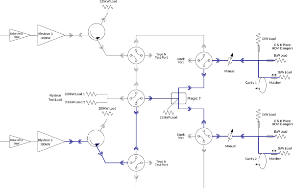
Table I shows typical values of storage ring (SR) RF power requirement for nominal user operation for both ALS at 1.9 Gev 500 mA multi bunch mode, and the planned ALS-Upgrade (ALS-U) project at 2.0 GeV.
| ALS | ALS-U | ||
| Number of Klystrons | 2 | ||
| Number of Cavities | 2 | ||
| Cavity | 28670 | ||
| Cavity | 16700 | ||
| Harmonic number | 328 | 327 | |
| Circumference | 196.8 | 195.94 | m |
| Beam energy | 1.9 | 2.0 | GeV |
| Cavity RF Frequency | 499.64 | 500.394 | MHz |
| (ea) | 4.9 | 4.9 | M |
| Cavity voltage | 671 | 300 | kV |
| 2.9 | 10.07 | ||
| Energy loss per trun | 329 | 329 | keV |
| BM Beam Power | 141 | 125 | kW |
| ID Beam Power | 42 | 35 | kW |
| 3HC Beam Power | 7.3 | 4.4 | kW |
| Parasitic Beam Power | 2.9 (est.) | 2.2 (est.) | kW |
| Total Beam Power | 192.9 | 166.9 | kW |
| Cavity Power(no beam) | 46 | 9.2 | kW |
| Cavity Power(beam) | 142.5 | 127.6 | kW |
| Waveguide Loss | 9.2 (est.) | 2.6 (est.) | kW |
| High Power Amplifier | 294.0 | 257.8 | kW |
As part of the ALS RF system upgrade project, the digital LLRF system was designed to replace the analog controller [1] and corresponding RF interlock systems, with design parameters and requirements listed in Table II. The digital LLRF system was installed and commissioned in March 2017, and was operational since then. It is expected that the current LLRF design would still meet ALS-U SR RF specifications, except ALS-U would have additional LLRF control requirements to its accumulator ring RF.
| Analog LLRF | Digital LLRF | ||
|---|---|---|---|
| Num. RF Drive Modes | 1 | 5 | |
| Num. RF Signals | 4 | 42 | |
| Amp. Loop Bandwidth | 3.5 | 1 | kHz |
| Phase Loop Bandwidth | 3.6 | 1 | kHz |
| Phase Jitter [10Hz,1MHz] | ps | ||
| Interlock latency | s | ||
| Amp. stability | 0.56 | % | |
| Phase stability | 1.8 | ∘ |
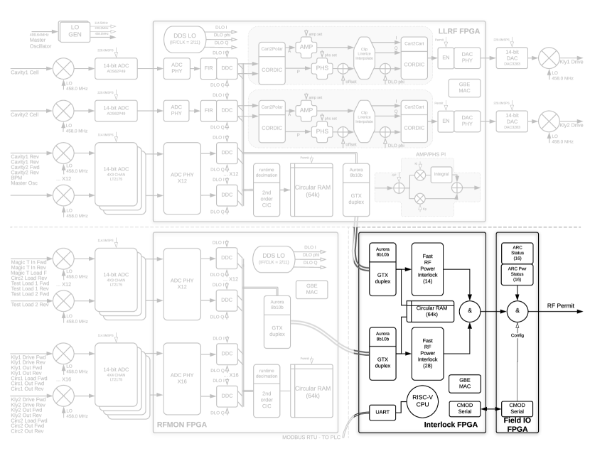
The digital LLRF consists of three connected FPGA chassis: LLRF chassis, RF monitor (RFMON) chassis and Fast Interlock chassis as shown in 2. The LLRF chassis generates a common LO reference from ALS master oscillator for synchronous digitizing and digital signal processing clocks for all 42 RF signals, and two processed IQ streams from LLRF and RFMON chassis are sent to Fast Interlock chassis for centralized interlock processing together with 16 channels of ARC detectors.
Each FPGA chassis has Gigabit Ethernet communication to a local computer that hosts EPICS Input-Output-Controller(IOC) to access all raw and processed registers, and configurable waveforms. Fast Interlock chassis has a dedicated communication to master interlock PLC, so that all interlock settings are directly available from PLC, which holds the RF drive mode and waveguide matrix configuration information.
The PLC-FPGA interlock system is designed to be software–free, so that the operation reliability and interlock invulnerability would not be impacted by external components such as EPICS, network or any operating system issues.
II Hardware design
II-A Frequency configuration
Both LO and sampling frequency are derived from ALS master oscillator .
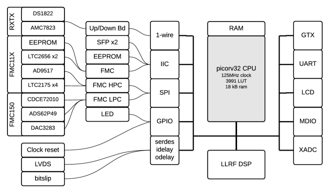
II-B Low-Level RF chassis
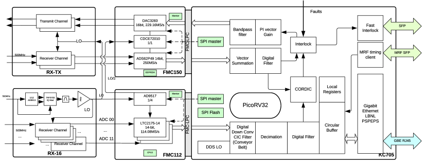
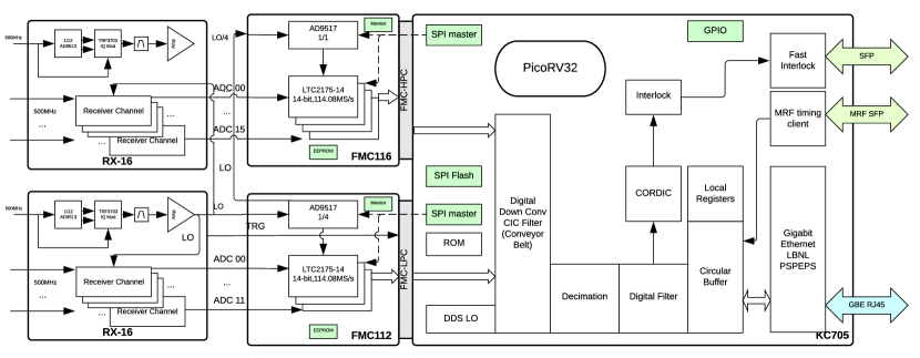
The LLRF chassis uses Abaco Systems FMC150 and FMC112 with Xilinx KC705 FPGA carrier board for digital platform. FMC150 provides 2 14-bits ADC and 2 16-bits DAC channels at for precision control, and FMC112 provides 12 14-bits ADC at for RF monitoring. Two Gigabit transceivers (GTX) links are used for inter–FPGA communication via optic fiber (SFP+) for interlocking and timing distribution respectively.
II-B1 Single Side Band LO generation
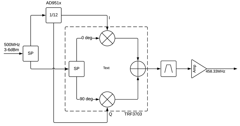
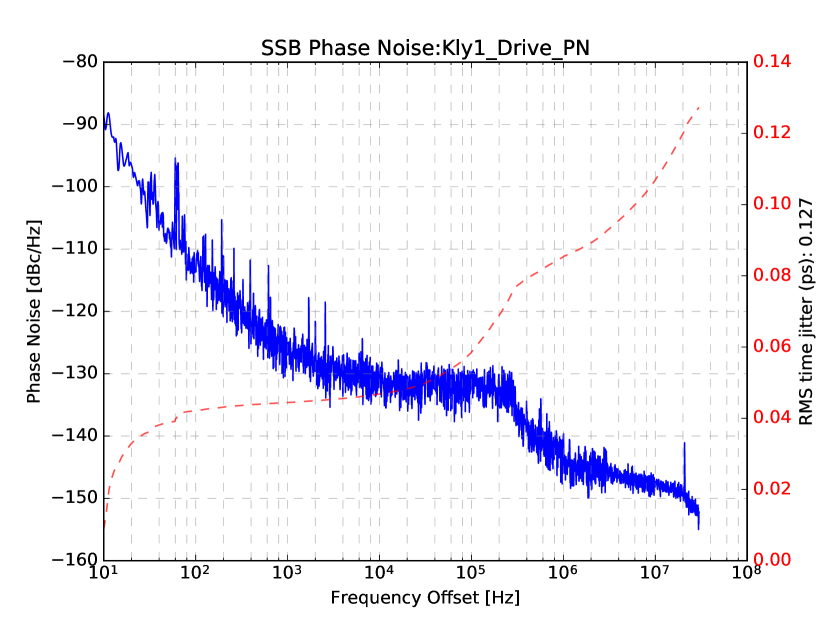
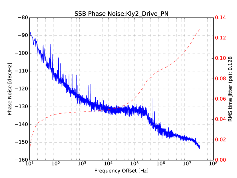
is generated using single side band modulation by a frequency divider AD9513 and a vector modulator TRF3703, as shown in Figure 4(a). Because both chips are not sensitive to clock signal level, the generated LO level is stable against MO signal level variations. The carrier feed through and image frequency suppression is also benefited as shown in Table III. When using an external signal source with 107 fs rms phase jitter at , the measured phase noise of is 140 fs rms [1Hz, 20MHz].
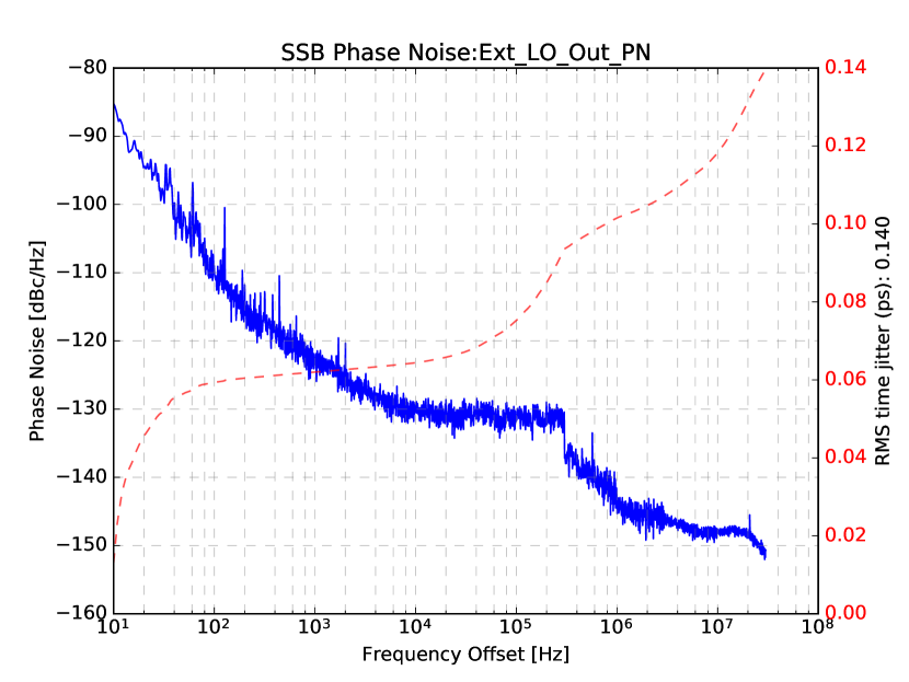
| Carrier feed–through | -45.4 | dB |
|---|---|---|
| Image frequency suppression | -59.3 | dB |
| LO phase jitter | 140 | fs (rms) |
| LO level variation over a week | dBm (p2p) |
II-B2 Analog RF Frontend
All RF signals are down converted to for digitization using a home-built analog frontend boards. A 16 channel down converter is designed in order to interface FMC112/FMC116 as shown in Figure 5.
This frontend board features single side band LO generation and distribution, externally synchronizable switch DC power supply, individual linear regulator for each channel, high channel isolations, and environmental monitoring for voltage, current, LO level and temperature.
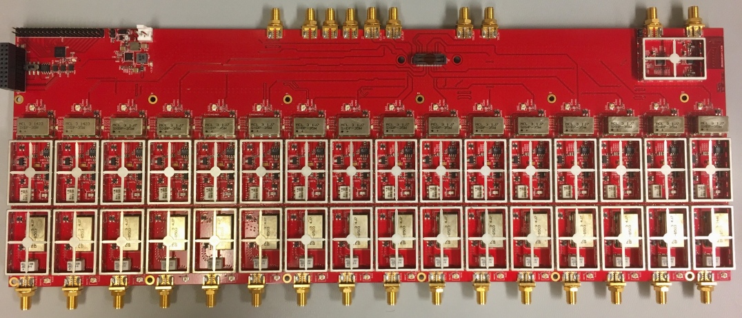
The cross talk between channels is optimized by using RF shielding, various attenuation and filtering in LO path, and individual low noise local voltage regulators. It is measured as better than 50 dB when using the high density connector for FMC112/FMC116.
II-B3 ADC benchmark
By injecting a near full scale signal at , all ADC channels including analog down conversion are benchmarked to match data sheet specifications.
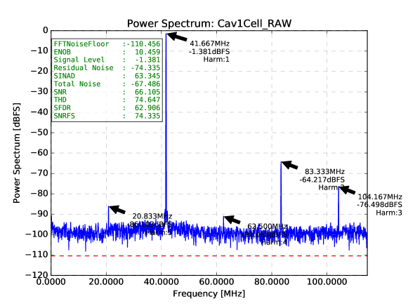
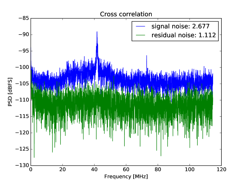
In order to separate signal against common components between ADC channels such as feedthrough, LO and common power supply noise, we used cross correlation between channel and to measure residual ADC noise [2].
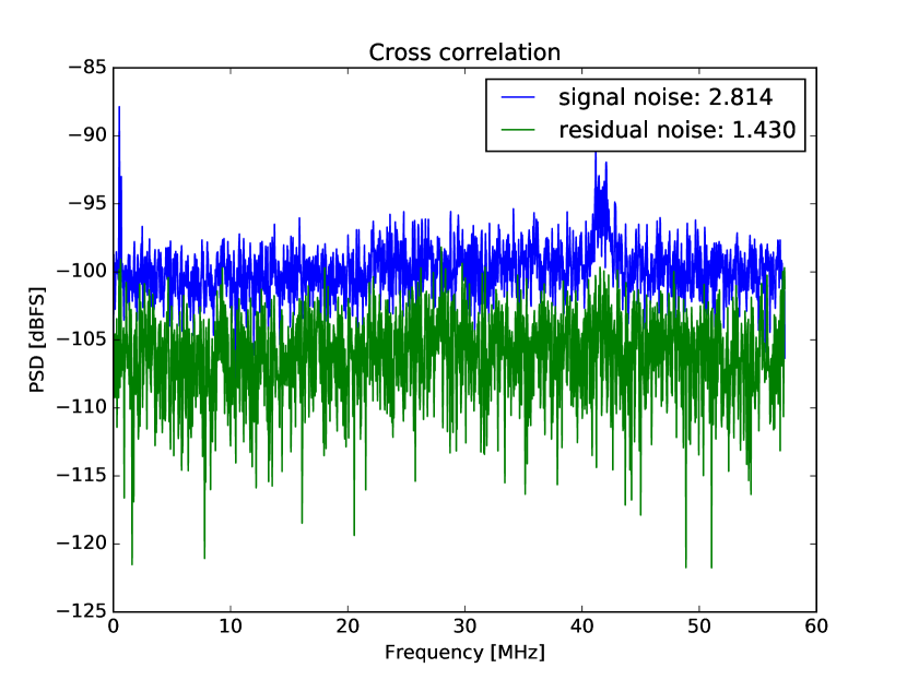
| Specified | Measured | ||
|---|---|---|---|
| Total SNR | 71 | 66 | dBFS |
| 75 | 74.34 | dBFS | |
| Isolation (feedback) | dB | ||
| Isolation (interlock) | 55 | dB |
It is concluded that the analog frontend together with digitization platform meets the design specifications.
II-B4 DAC benchmark
The phase noise of two DAC output signal at after up conversion are measured as fs (rms) [1Hz, 20MHz] using a signal source analyzer (Rohde & Schwarz FSUP) which also met design specification, as shown in Figure 8.
II-C RF Monitor chassis
The RF monitor chassis uses Abaco Systems FMC112 and FMC116 with Xilinx KC705 FPGA carrier, as in Figure 9. Two 16–channel down conversion frontend boards are used to host 28 channels. LO signal are from LLRF chassis to keep the same frequency divider states for RF phase measurement. All sampling frequencies are at and FPGA clock is running at twice as fast at . The communication interfaces are common to LLRF chassis.
II-D Fast Interlock Chassis
Also based on Xilinx KC705, the Fast Interlock Chassis uses two GTX links to collect and process IQ streams from LLRF and RFMON chassis, with addition of 16 channels of arc detectors faults and arc power faults through a Field IO FPGA (Digilent CMOD S6). The standalone reference clock is tuned to be within ppm of stream clock at .
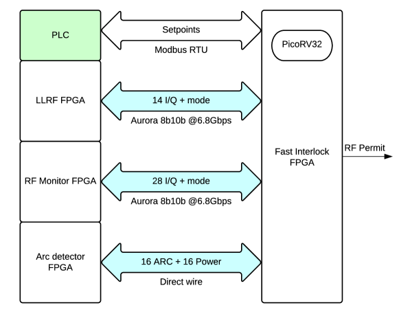
All interlock configurations and setpoints are passed by PLC–FPGA communication, and the end–to–end interlock latency needs to be s.
III Firmware design
III-A Digital Signal processing
III-A1 Direct Digital Down-conversion
Non–IQ sampling avoids aliasing for high precision digitization.[3] In our case, with , one can construct direct digital down–conversion (DDC) using two consecutive ADC samples . The coefficient matrix is generated using a Coordinate Rotation Digital Computer (CORDIC).
III-A2 Double-time signal process
Because , and also the need for dynamically configure feedback signal paths according to RF drive mode, it is desired to have two DSP clock cycles per ADC sample in order to reuse the same pipeline for different combinations of RF signal processing. Figure 11 shows an example of pipe lining two ADC channels to a stream of digitally down converted IQ pairs.

III-A3 Feedback controller
The feedback controller is constructed as shown in Figure 12.
The framed IQ pairs, in our case two cavity probe signals are converted to amplitude and phase in order to compare with loop sepoints, and fed into a set of proportional–integral controllers with limiter. The clipped output is then digitally up converted using an output CORDIC with an optional phase shifter to compensate variable loop group delay. When RF permit signal is valid, the loop output signal is sent to each DAC.
There are amplitude and phase loops for each klystron. For one klystron driving two cavities of test loads, the weighted average of two cavity probe amplitudes are used for amplitude loop, and one cavity phase for phase loop.
Since the exact controller transfer function is known by design, the loop register scaling are verified using an IIR cavity emulator in domain.

III-A4 Waveform
All baseband signal after DDC are serialized onto a conveyor belt signal stream to apply a run–time configurable CIC filter for different decimation factors.

Features of waveform handling includes dynamic channel selection, collision–free doubled buffer structure, associated statistics with timestamps, and fault capturing.

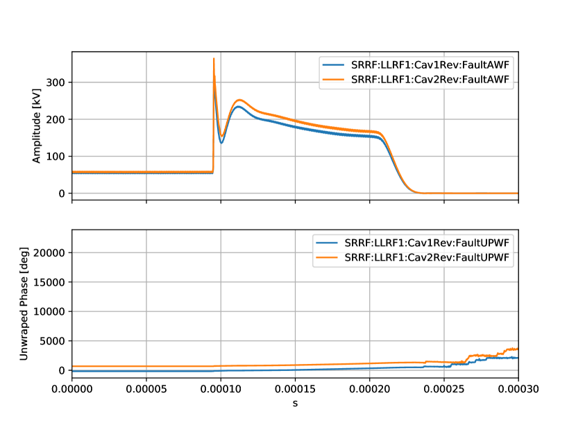
Figure 14 shows an example of fault waveform capturing at an event of RF trip, when both cavities were only driven by beam after LLRF permit was removed. This is an essential feature for finding the root cause of RF system trip.
III-A5 Peripheral management
There are hundreds of registers and complicated processes involved in initialization process to bring the system to nominal state from power up. An open source RISC–V soft core PicoRV32[4] is used in each design to handle peripheral management and initialization process.
III-A6 PLC–FPGA interface
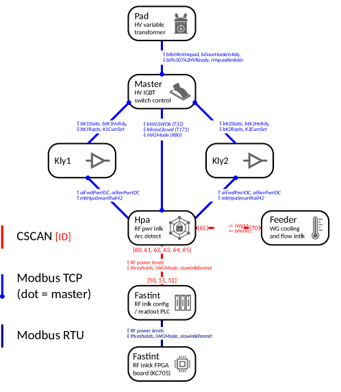
PicoRV32 in Fast Interlock Chassis also handles direct interfacing with PLC via ModbusRTU. The multi-chassis FPGA system works as a peripheral from PLC point of view as shown in Figure 16.
IV Software design
Both python based diagnostic tools and EPICS based operation applications were developed based on the UDP Gigabit direct access to registers and waveforms [5].
V Operation and performance
V-A RF stability
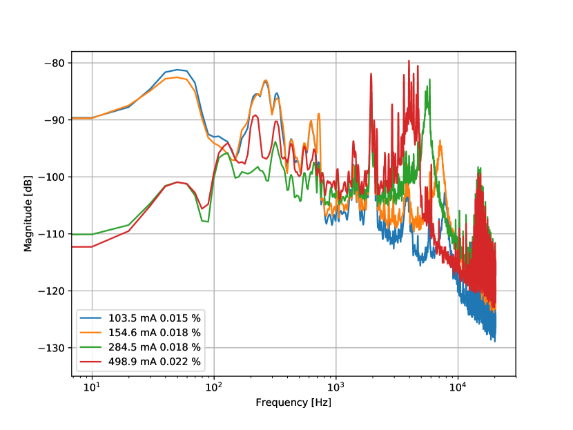
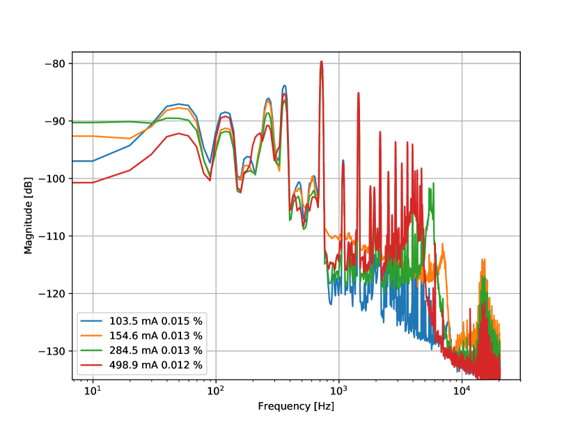
We have measured both amplitude and phase loop noise spectrum density from in–loop waveform data at different beam currents as shown in Figure 17. The data was measured under klystron 2 drive mode, where average of two cavity cell voltages are regulated. Loop parameters are at operation nominal setting, with kHz bandwidth, integral only. It is observed that, as beam current increased from 103 mA to 499 mA, the synchrotron frequency moved from kHz towards kHz, and its contribution became more significant. Within analyse bandwidth of [10Hz, 20kHz], the amplitude loop stability is measured as rms, and phase loop stability is rms.
V-B Loop Frequency Response
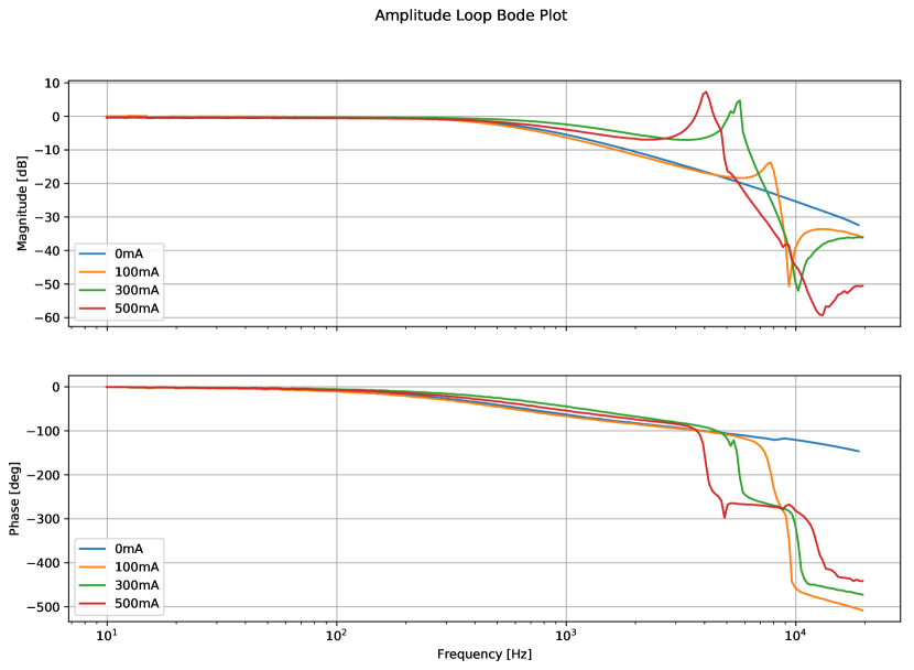
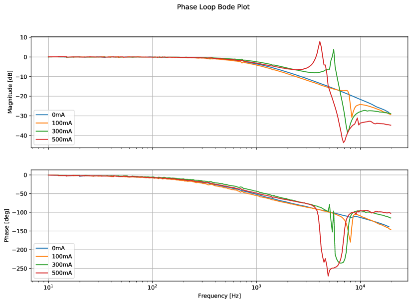
By injecting a excitation tone on either amplitude or phase loop setpoint, the closed loop frequency response could be measured as a function of excitation frequency. We have measured bode plots at different beam currents as shown in Figure 18. Both amplitude and phase loop unity gain is observed around 1 kHz, as expected. Again, beam induced synchrotron frequencies contributes as a resonance peak outside loop bandwidth.
V-C Hard real–time RF interlock
| RF Power (Lab) | 1.45 | s |
|---|---|---|
| RF Power (ALS) | s | |
| ARC det. latency | s |
VI Conclusion
The digital LLRF system for ALS storage ring RF is operational since March 2017 with months of mean time between failure. System functionality and performance met design requirements.
Acknowledgment
This work is supported by the Office of Science, Office of Basic Energy Sciences, of the U.S. Department of Energy under Contract No. DE-AC02-05CH11231.
References
- [1] C. Lo, B. Taylor, and K. Baptiste, “The amplitude and phase control of the als storage ring rf system,” in Proceedings Particle Accelerator Conference, vol. 2. IEEE, 1995, pp. 801–803.
- [2] L. Doolittle, G. Huang, K. Campbell, E. Cullerton, and J. Jones, “LCLS–II LLRF Loopback Test Results,” 2016, http://recycle.lbl.gov/~ldoolitt/loopback.
- [3] L. Doolittle, H. Ma, and M. S. Champion, “Digital Low–Level RF Control using Non–IQ Sampling,” in Proceedings of LINAC 2006, Knoxville, Tennessee USA. Citeseer, 2006, pp. 568–570.
- [4] C. Wolf, “PicoRV32 – A Size–Optimized RISC–V CPU,” https://github.com/cliffordwolf/picorv32, 2015.
- [5] C. Serrano and L. Doolittle, “FPGA Communications based on Gigabit Ethernet,” in 13th International Conference on Accelerator and Large Experimental Physics Control Systems 2011, Grenoble, France, 2011.