Gate field effects on the topological insulator interface
Abstract
Interfaces between two topological insulators are of fundamental interest in condensed matter physics. Inspired by experimental efforts, we study interfacial processes between two slabs of (BSTS) via first principles calculations. Topological surface states are absent for the BSTS interface at its equilibrium separation, but our calculations show that they appear if the inter-slab distance is greater than . More importantly, we find that topological interface states can be preserved by inserting two or more layers of hexagonal boron nitride between the two BSTS slabs. In experiments, the electric current tunneling through the interface is insensitive to back gate voltage when the bias voltage is small. Using a first-principles based method that allows us to simulate gate field, we show that at low bias the extra charge induced by a gate voltage resides on the surface that is closest to the gate electrode, leaving the interface almost undoped. This provides clues to understand the origin of the observed insensitivity of transport properties to back voltage at low bias. Our study resolves a few questions raised in experiment, which does not yet offer a clear correlation between microscopic physics and transport data. We provide a road map for the design of vertical tunneling junctions involving the interface between two topological insulators.
Topological surface states (TSS) of a three dimensional topological insulator (TI) have drawn much research attention due to their robustness, linear dispersion, and spin-momentum locking, which allow potential applications in low-energy-consumption electronics and spintronics Hsieh2012 ; Chen2012 . A large category of electronic/spintronic devices involve an interface between a TI and another material, which could be a normal insulator, metal, magnet, superconductor, or even molecules Gehring2012 ; Berntsen2013 ; Yoshimi2014 ; Seibel2012 ; NKim2013 ; Scholz2012 ; Shoman2015 ; JLi2012 ; MLi2015 ; LFu2006 ; Jauregui2018 ; JZhang2016 ; Jakobs2015 . It is thus necessary to understand how TSS are affected by proximity effects, especially their preservation Gehring2012 ; Berntsen2013 ; Yoshimi2014 ; Seibel2012 ; NKim2013 ; Scholz2012 ; Shoman2015 or passivation Berntsen2013 ; JZhang2016 ; Jakobs2015 . A gate field is often applied to control the electron transport properties of an electronic device. A single gate induces charge doping, and a dual gate configuration can further create a vertical electric field. A gate voltage provides a knob for tuning topological surface/interface states Steinberg2010 ; Sulaev2015 ; YXu2015 . Nevertheless, theoretical work has been mostly limited to model JLi2009 ; Yokoyama2010 or conventional electronic structure calculations. Min2007 ; Houssa2016
(BSTS) has been reported to be topological insulator with high bulk resistivity and robust surface states for certain and values AATaskin2011 ; TArakane2012 ; YXu2014 ; HLohani2017 . In this work, we study the interface between two slabs, with and without spacers in between. We construct a theoretical approach that can simulate gate effects via a first-principles treatment. The major results reported here are from theoretical investigations which are motivated by the experimental data. Experimentally, two BSTS flakes are prepared separately before stacked together to form a vertical tunneling junction. It is observed that the electric current is not sensitive to a back gate voltage when the bias voltage between the two BSTS slabs is small (see Fig. S1 in the supplemental material). Based on these observations, theoretical investigations focus on the three questions – First, do topological interface states exist at the BSTS interface? Second, how do topological interface states respond to a gate field when they are present? and, Third, how can we turn BSTS into a quantum system that is useful for future electronics? This work offers a picture at the electron level, deepens our understanding of TI interfaces and demonstrates a way to utilize quantum TSS, and finally provides an idea for designing TI-based vertical tunneling devices.

In order to answer whether the interface hosts topological surface states, we first generate a special quasirandom structure of the BSTS alloy, that approximates the true disordered state with a periodic supercell deWalle2013 , using the “mcsqs” code of the Alloy Theoretic Automated Toolkit deWalle2013 ; deWalle2002 . The topological invariants of our quasirandom BSTS supercell are calculated to be with the aid of the Z2Pack package. Gresch2017 ; Soluyanov2011 As such, our model BSTS represents a strong topological insulator. Then, we build a BSTS interface based on the special quasirandom structure and visualize it using the Visualization for Electronic and Structural Analysis (VESTA) software Momma2011 . As shown in Fig. 1, the interface is made of two BSTS slabs that are separated by distance , where each slab contains six quinlayers, periodic in the - plane perpendicular to the -direction. The in-plane lattice constants are and , with . At least of vacuum is added along the -direction to avoid interaction between periodic images of the same system. For a single BSTS slab with six quinlayers, we test that there are localized surface states with spin-momentum locking that disappear if spin-orbit coupling is switched off, evidence that the special random structure represents a topological insulator. Our calculations are based on density functional theory (DFT) HK1964 ; KS1965 as implemented in the Vienna Ab initio simulation package (VASP). KH1993 ; GKresse1999 In VASP calculations, we adopt at least a energy cutoff for plane waves, the PAW pseudopotential PEBlochl1994 ; GKresse1999 , the optB86b vdW-DF energy functional for including the van der Waals interaction MDion2004 ; GRP2009 ; JKlimes2010 , a Monkhorst-Pack -point mesh, a energy tolerance for self-consistency, and a force tolerance for ionic relaxation.
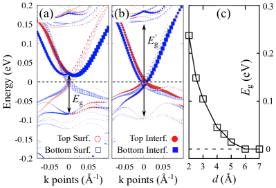
Now, we examine the relation between interface states and the inter-slab distance . Figs. 2(a) and 2(b) show the band structure of the BSTS interface with an inter-slab distance of and respectively. For both and , the top (bottom) surface band forms a Dirac cone around the Fermi energy. In contrast, for , the top (bottom) interface band does not form a Dirac cone, and an energy gap of opens at the point. This energy gap however closes when , due to weak interaction between the two slabs, and accordingly the Dirac cone for the top (bottom) interface is recovered. Therefore, the presence of topological interface states strongly depends on the inter-stab distance . Fig. 2(c) shows that decreases with and reaches zero at around . Note that there are three typical alignments of stacking between the two BSTS slabs, namely the atop, the bridge and the hollow. The above discussion is for the BSTS interface with atop stacking; however it remains valid qualitatively for the other two stackings. The energetically favorable for the atop (the bridge, the hollow) stacking is about (, ) Å and a Dirac cone is not formed. The hollow site stacking is the most stable configuration, about and lower than the bridge stacking and the atop stacking respectively.
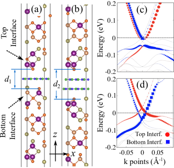
In order to recover TSS at the interface, we considered inserting -BN between the two BSTS slabs, since -BN is a normal insulator WAuwarter2004 and TSS are known to exist at the interface between a topological insulator and a normal insulator Gehring2012 (experimentally, it might be easier to prepare BSTS with a surface covered by a -BN monolayer before stacking two pieces together). In the following, we show that monolayer -BN is not sufficient, and two layers of -BN are required. Fig. 3(a) [3(b)] shows the atomic configuration of the BSTS interface with monolayer (bilayer) -BN, denoted as BSTS/BN/BSTS (BSTS/BN/BSTS). The band structures for BSTS/BN/BSTS and BSTS/BN/BSTS are shown in Figs. 3(c) and 3(d). The red circles (blue squares) are for the top (bottom) interface and again the size of a circle/square indicates the localization of the corresponding state. When there is only one layer of -BN, a band gap opens at the point for both the top and the bottom interface states around the Fermi energy. In other words, Dirac cone and TSS are absent at the interface. In contrast, when there are two layers of -BN, the energy gap closes and two Dirac cones are formed around Fermi energy, one for the top interface states and the other for the bottom interface states. These results are for hollow stacking between BSTS and BN; however they remain valid for atop stacking and bridge stacking. We observe that the top (bottom) interface is slightly hole- (electron-) doped. This charge transfer arises from the asymmetry in the atomic configuration of the interface. If we construct an inversion symmetric interface, then the two Dirac cones indeed become identical and the Dirac points are located at the Fermi level. Note that the top and the bottom surface states still exist, although they are not emphasized in Fig. 3.
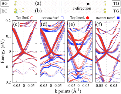
So far, we have answered the question of whether or not TSS exist at the BSTS interface. Now we turn to the second question: How do topological interface states respond to a gate field? In order to answer this question, we take the BSTS/BN/BSTS interface as an example and place it between two gate electrodes, as shown in Fig. 4. Each gate electrode has a constant Hartree potential and the two gate electrodes could have different Hartree potentials, forming a non-periodic boundary condition. We simulate the gate field effect using the Effective Screening Medium (ESM) method as implemented in the SIESTA package ESM ; SIESTA , where the non-periodic boundary condition for the Hartree potential is dealt with Green’s functions. A vacuum layer of about nm thick is inserted between the BSTS slab and the top/bottom gate electrode as a dielectric layer. We adopt norm-conserving relativistic pseudopotentials as generated via the Troullier-Martins scheme of the “atom” code NTroullier1991 ; ATOM . The pseudopotentials for Bi, Se and Te atoms are created by Rivero et al. PRivero2015 and the rest ones are created by the authors. The localized basis set is optimized in order to obtain a reasonable band structure compared with the results of VASP. We use the PBE exchange correlation energy functional. This does not present a problem because the atomic structure is fixed and van der Waals interaction does not change the band structure much. A mesh cutoff of is used to sample in real space.
Two gate electrodes permit not only charge doping but also an electric field perpendicular to the interface. Here electric field means the average electric field between the two gate electrodes,
| (1) |
where is the Hartree potential difference between the top and bottom gate electrodes and is the distance between the two gate electrodes. The electric field in the caption of Fig. 4 also means that in Eq. (1). Fig. 4(a) and 4(b) show the charge redistribution across the BSTS interface when it is doped with extra electrons note1 and subject to zero electric field. In Fig. 4(a), the BSTS interface with bilayer -BN is doped with unit charges per unit cell. The corresponding carrier density is about , where is the surface area of a unit cell. As seen from the figure, the extra electrons are mainly located at the top and the bottom surfaces, while the inner part of the system is hardly doped. For a single gate configuration, the extra charge goes mainly to the surface that is closest to the gate electrode. As such, the local electronic structure at the interface does not change much, and it might be a reason for the insensitivity of the electric current to the gate voltage at small bias voltage. In Fig. 4(b), the net charge per cell is . In this case, compared with Fig. 4(a) the extra electrons spread more into the inner part of the heterostructure. In order to understand this, we plot the band structures of the BSTS interface with different net charges in Figs. 4(c)–(f). As shown In Fig. 4(c), without charge doping there are four Dirac cones around the Fermi energy for, respectively, the top surface, the top interface, the bottom interface, and the bottom surface, In Fig. 4(d), the system is doped with electrons () per unit cell, and these electrons fill into the two Dirac cones for the the top and the bottom surfaces, leaving the remaining two Dirac cones undoped. This is consistent with the charge redistribution shown in Fig. 4(a). It can also be seen from Fig. 4(d) that the bulk energy bands above the Fermi energy move downwards. At yet higher doping levels such as in Fig. 4(e), the surface energy bands are filled with more electrons and the bulk energy bands move even closer to the Fermi energy. Eventually the bulk energy bands reach the Fermi energy and thus are also doped, as seen in Fig. 4(f) where . Under certain doping levels, the charge distribution of the BSTS interface with bilayer -BN can be further tuned by the electric field between the two electrodes. In the case of , a small electric field along the -direction moves electrons from the top surface to the bottom surface, and the inner part of the system is not doped until is greater than . This may be related to the increased sensitivity of the electric current to the gate voltage at higher bias voltages, as shown in Fig. S1 (see supplemental information).
In conclusion, we have a clear microscopic picture of the interface between two slabs of the topological insulator . We find that topological interface states are absent unless the inter-slab distance is greater than ; they can however be preserved by two or more layers of -BN that serves as a spacer between the two BSTS systems, which is verified by our calculations and is the answer to the third question imposed at the beginning of this paper. We undercover the mechanism underlying physical processes in small and large doping levels and provide clues to understand electron transport characteristics in the BSTS vertical tunneling junction configuration. The combination of a -BN spacer and single/double gating is a promising way to protect TSS and modify interfacial electronic processes.
See the supplemental information for electron transport measurement of a BSTS vertical tunneling junction, energy bands and hybrid Wannier charge centers of the quasirandom BSTS, results for different stackings between a BSTS slab and another BSTS slab or a BN layer, charge distribution for a single gate configuration, effect of electric field on the BSTS interface, parameters for basis set and pseudopotentials etc.
This work is supported by the US Department of Energy (DOE), Office of Basic Energy Sciences (BES), under Contract No. DE-FG02-02ER45995. Y. P. C. acknowledges partial support from National Science Foundation (NSF) under Grant No. EFMA-1641101. Computations were done using the utilities of the National Energy Research Scientific Computing Center and University of Florida Research Computing.
References
- (1) D. Hsieh, Y. Xia, D. Qian, L. Wray, J. H. Dil, F. Meier, J. Osterwalder, L. Patthey, J. G. Checkelsky, N. P. Ong, A. V. Fedorov, H. Lin, A. Bansil, D. Grauer, Y. S. Hor, R. J. Cava, and M. Z. Hasan, Nature 460, 1101–1106 (2009).
- (2) Y. P. Chen, Proc. SPIE 8373: Micro- and Nanotechnology Sensors, Systems, and Applications IV, 83730B (2012).
- (3) P. Gehring, B. F. Gao, M. Burghard, and K. Kern, Nano Lett. 12, 5137–5142 (2012).
- (4) M. H. Berntsen, O. Götberg, B. M. Wojek, and O. Tjernberg, Phys. Rev. B 88, 195132 (2013).
- (5) R. Yoshimi, A. Tsukazaki, K. Kikutake, J. G. Checkelsky, K. S. Takahashi, M. Kawasaki, and Y. Tokura, Nat. Mater. 13, 253–257 (2014).
- (6) C. Seibel, H. Maaß, M. Ohtaka, S. Fiedler, C. Jünger, C.-H. Min, H. Bentmann, K. Sakamoto, and F. Reinert, Phys. Rev. B 86, 161105(R) (2012).
- (7) N. Kim, P. Lee, Y. Kim, J. S. Kim, Y. Kim, D. Y. Noh, S. U. Yu, J. Chung, and K. S. Kim, ACS Nano 8, 1154–1160 (2013).
- (8) M. R. Scholz, J. Sánchez-Barriga, D. Marchenko, A. Varykhalov, A. Volykhov, L. V. Yashina, and O. Rader, Phys. Rev. Lett. 108, 256810 (2012).
- (9) T. Shoman, A. Takayama, T. Sato, S. Souma, T. Takahashi, T. Oguchi, K. Segawa, and Y. Ando, Nat. Commun. 6, 6547 (2015).
- (10) J. Li, Z. Y. Wang, A. Tan, P.-A. Glans, E. Arenholz, C. Hwang, J. Shi, and Z. Q. Qiu, Phys. Rev. B 86, 054430 (2012).
- (11) M. Li, C.-Z. Chang, B. J. Kirby, M. E. Jamer, W. Cui, L. Wu, P. Wei, Y. Zhu, D. Heiman, J. Li, and J. S. Moodera, Phys. Rev. Lett. 115, 087201 (2015).
- (12) L. Fu and C. L. Kane, Phys. Rev. Lett. 10, 096407 (2008).
- (13) L. A. Jauregui, M. Kayyalha, A. Kazakov, I. Miotkowski, L. P. Rokhinson, and Y. P. Chen, Appl. Phys. Lett. 112, 093105 (2018).
- (14) J. Zhang, J. P. Velev, X. Dang, and E. Y. Tsymbal, Phys. Rev. B 94, 014435 (2016).
- (15) S. Jakobs, A. Narayan, B. Stadtmúller, A. Droghetti, I. Rungger, Y. S. Hor, S. Klyatskaya, D. Jungkenn, J. Stöckl, M. Laux, O. L. A. Monti, M. Aeschlimann, R. J. Cava, M. Ruben, S. Mathias, S. Sanvito, and M. Cinchetti, Nano Lett. 15, 6022–6029 (2015).
- (16) H. Steinberg, D. R. Gardner, Y. S. Lee, and P. Jarillo-Herre, Nano Lett. 10, 5032–5036 (2010).
- (17) A. Sulaev, M. Zeng, S.-Q. Shen, S. K. Cho, W. G. Zhu, Y. P. Feng, S. V. Eremeev, Y. Kawazoe, L. Shen, and L. Wang, Nano Lett. 15, 2061–2066 (2015).
- (18) Y. Xu, I. Miotkowski, and Y. P. Chen, Nat. Commun. 7, 11434 (2015).
- (19) J. Li and K. Chang, Appl. Phys. Lett. 95, 222110 (2009).
- (20) T. Yokoyama, A. V. Balatsky, and N. Nagaosa, Phys. Rev. Lett. 104, 246806 (2010).
- (21) H. Min, B. Sahu, S. K. Banerjee, and A. H. MacDonald, Phys. Rev. B 75, 155115 (2007).
- (22) M. Houssa, B. van den Broek, K. Iordanidou, A. K. Augustin Lu, G. Pourtois, J.-P. Locquet, V. Afanas’ev, and A. Stesmans, Nano Research 9, 774–778 (2016).
- (23) A. A. Taskin, Z. Ren, S. Sasaki, K. Segawa, and Y. Ando, Phys. Rev. Lett. 107, 016801 (2011).
- (24) T. Arakane, T. Sato, S. Souma, K. Kosaka, K. Nakayama, M. Komatsu, T. Takahashi, Z. Ren, K. Segawa, and Y. Ando, Nat. Commun. 3, 636 (2012).
- (25) Y. Xu, I. Miotkowski, C. Liu, J. Tian, H. Nam, N. Alidoust, J. Hu, C.-K. Shih, M. Z. Hasan, and Y. P. Chen, Nat. Phys. 10, 956–963 (2014).
- (26) H. Lohani, P. Mishra, A. Banerjee, K. Majhi, R. Ganesan, U. Manju, D. Topwal, P. S. Anil Kumar, and B. R. Sekhar, Sci. Rep. 7, 4567 (2017).
- (27) A. van de Walle, P. Tiwary, M. de Jong, D.L. Olmsted, M. Asta, A. Dick, D. Shin, Y. Wang, L.-Q. Chen, Z.-K. Liu, CALPHAD J. 42, 13–18 (2013).
- (28) A. van de Walle, M. Asta, G. Ceder, CALPHAD J. 26, 539–553 (2002).
- (29) D. Gresch, G. Autès, O. V. Yazyev, M. Troyer, D. Vanderbilt, B. A. Bernevig, and A. A. Soluyanov, Phys. Rev. B 95, 075146 (2017).
- (30) A. A. Soluyanov and D. Vanderbilt, Phys. Rev. B 83, 235401 (2011).
- (31) K. Momma and F. Izumi, J. Appl. Crystallogr. 44 1272–1276 (2011).
- (32) P. Hohenberg and K. Walter, Phys. Rev. 136, B864–B871 (1964).
- (33) W. Kohn and L. J. Sham, Phys. Rev. 140, A1133–A1138 (1965).
- (34) G. Kresse and J. Hafner, Phys. Rev. B 47, 558 (1993).
- (35) G. Kresse and D. Joubert, Phys. Rev. B 59, 1758 (1999).
- (36) P. E. Blöchl, Phys. Rev. B 50, 17953 (1994).
- (37) M. Dion, H. Rydberg, E. Schröder, D. C. Langreth, and B. I. Lundqvist, Phys. Rev. Lett. 92, 246401 (2004).
- (38) G. Román-Pérez and J. M. Soler, Phys. Rev. Lett. 103, 096102 (2009).
- (39) J. Klimeš, D. R. Bowler, and A. Michaelides, J. Phys.: Cond. Matt. 22, 022201 (2010).
- (40) W. Auwärter, H. U. Suter, H. Sachdev, and T. Greber, Chem. Mater. 16, 343–345 (2004).
- (41) M. Otani and O. Sugino, Phys. Rev. B 73, 115407 (2006).
- (42) J. M. Solar, E. Artacho, J. D. Gale, A. García, J. Junquera, P. Ordeón, and D. Sánchez-Portal, J. Phys. Condens. Matter 14, 2745 (2002).
- (43) N. Troullier and J. L. Martins, Phys. Rev. B 43, 1993 (1991).
- (44) ATOM, a program for DFT calculations in atoms and pseudopotential generation, maintained by Alberto Garcia.
- (45) P. Rivero, V. M. García-Suárez, D. Pereñiguez, K. Utt, Y. Yang, L. Bellaiche, K. Park, J. Ferrer, S. Barraza-Lopez, Comput. Mater. Sci. 98, 372–389 (2015).
- (46) Since the TSS below the Fermi energy are not very accurate in SIESTA compared with VASP, we will consider only electron doping in the following.