3D Field Simulation Model for Bond Wire On-Chip Inductors Validated by Measurements
Abstract
This paper proposes 3D field simulation models for different designs of integrated bond wire on-chip inductors. To validate the simulation models, prototypes for three designs with air and ferrite cores are manufactured and measured. For air core inductors, high agreement between simulation and measurement is obtained. For ferrite core inductors, accurate models require an exact characterization of the ferrite material. These models enable the prediction of magnetic field influences on underlying integrated circuits.
Index Terms:
Bond wire inductor, electromagnetic simulation, modeling.I Introduction
Inductors are critical components in most power electronic and radio-frequency (RF) circuits. However, their integration with the goal of high inductances on small areas remains an ongoing research topic [1]. A common approach for RF integrated circuits (ICs) is to realize inductances by 2D integrated planar spiral inductors [2]. These inductors are easy to implement and compatible for every process. However, this approach requires a high area consumption [3]. Moreover, the magnetic flux is perpendicular to its substrate causing possible interferences with the circuit within the IC.
For power applications, high inductances and high quality-factors (Q-factors) are required. Thus, the trend to miniaturization leads to an increasing research on power supply on chip (PwrSoC) with focus on inductors and transformers [4, 1, 5]. To obtain the required high inductances for power applications, discrete semiconductors are more promising than 2D spiral integrated inductors [4]. In particular, the fabrication of on-chip inductors and transformers using bond wires around a magnetic core is a promising approach [6, 7, 8]. Since the bonding process is a common subsequent process step after IC fabrication, this approach results in low additional costs and a low production time [9]. In addition, these components are less area consuming yielding a high power density and efficiency.
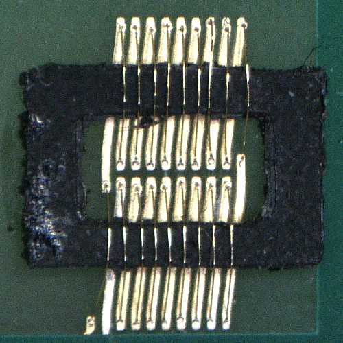
To reduce the number of prototypes, IC designers rely on simulation tools that require reliable inductor and transformer models. This work proposes bond wire on-chip inductors to be designed with the help of 3D field simulation. To test different geometric and material parameters without having to fabricate additional prototypes, simulation models were set up and validated using measurements of corresponding prototypes, such as the one in Fig. 1.
The paper is structured as follows. First, Section II introduces the simulation model to yield the resistance and inductance of an inductor. Then, Section III presents the prototypes and the measurement setup. Section IV discusses the results focusing on the comparison between measurement and simulation and Section 8 concludes the paper.
II Simulation Model
To avoid the costly fabrication of prototypes, simulation models were set up to predict the devices’ behavior. In this paper, the major quantities of interest are the resistance and the inductance of the on-chip inductor. This allows to consider appropriate stationary simplifications of Maxwell’s equations [10]. First, to compute the DC resistance, one needs to solve the electrokinetic problem
| (1) |
with magnetic boundary conditions and, e.g., and at the contacts. Here, is the electric scalar potential and is the electric conductivity. Then, the current can be computed, where is the cross-sectional area of a bond wire. Therefore, the DC resistance yields . Secondly, the inductance can be calculated from the magnetostatic field that is obtained from
| (2) |
where is the reluctivity, is the magnetic vector potential, and is a winding function that distributes the current accordingly. From , the magnetic field and the magnetic flux density are obtained by . Then, the magnetic energy is calculated by
where is the volume in which the energy shall be evaluated, and the inductance reads . Therefore, computing the resistance and the inductance of an on-chip inductor boils down to solving (1) and (2). For this purpose, CST EM STUDIO is used.
III Prototypes and Measurement Setup
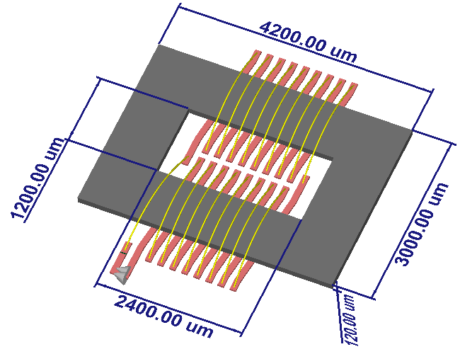
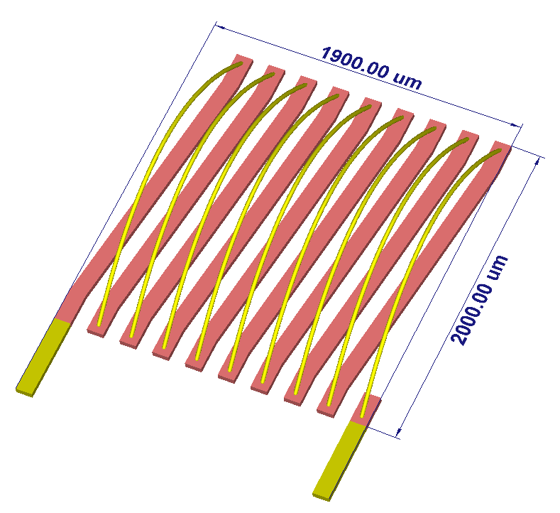
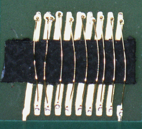
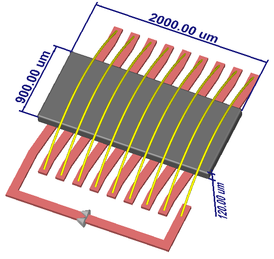
Three different bond wire inductor models and one bond wire transformer model were fabricated on a printed circuit board (PCB). Model A is an air core solenoid inductor with windings and a total footprint of , see Fig. 2a. Model B differs from model A only in an additional ferromagnetic core material as shown in Fig. 2b. Model C consists of a closed ferromagnetic core with two bond wire inductors in series that are placed on opposite legs of the ferromagnetic core. Each of the two inductors consists of windings and model C has a total footprint of as shown in Fig. 1. Table I summarizes the different parameters for the three models. Finally, the transformer model was realized by omitting the wires that connects the two serial inductors in model C.
| Model | in | Core | |
|---|---|---|---|
| Model A | 9 | 3.8 | Air |
| Model B | 9 | 3.8 | Bar ferrite |
| Model C | 18 | 16.8 | Closed ferrite |
The solenoid inductors and the transformer were fabricated using gold wires with a diameter of on a PCB with thick and wide copper traces and an electroless nickel electroless palladium immersion gold (ENEPIG) surface plating. For models B and C, the magnetic core consists of a ferrite foil which was trimmed using a laser cutter. Its initial relative permeability is given by at [11].

The impedance of the inductors were measured by an Agilent E5062A network analyzer which is capable of measuring S-parameters up to . Input and output reflections are reduced by a matching network built around the inductor (device under test) , see Fig. 3. To avoid reflections, resistor values of , and were chosen such that an input and output impedance of was obtained. To compensate parasitic influences of the PCB and the cables, a differential measurement method was used. Therefore, a matching circuit with a reference resistor is connected in parallel to the test channel.
Relating the measured forward voltage gain at the test channel to the one at the reference channel denoted by , the impedance is determined by
| (3) |
For frequencies far below the resonance frequency of the coil, the inductance can be calculated by
| (4) |
The Q-factor is given by [12]
| (5) |
The DC resistances of the prototypes were measured with a 4-wire sensing Keysight 34465A multimeter.

IV Results and Discussion
In this section, the results of the measurements and simulations are presented. First, the complex impedance has been measured at an input power of . It is shown for the three different models with respect to frequency in Fig. 4. As expected, the frequency dependent losses of the core material [11] result in an increase of Re() at higher frequencies for models B and C. On the other hand, only a slight increase with frequency is observed for the coreless model A. The inductances and Q-factors were extracted from S-parameter measurements and are shown with respect to frequency in Fig. 5a and Fig. 5b, respectively. The ferrite core of models B and C leads to a significant increase in inductance, see Fig. 5a. However, due to the losses in the core, only a small increase of the Q-factor is observed, see Fig. 5b.


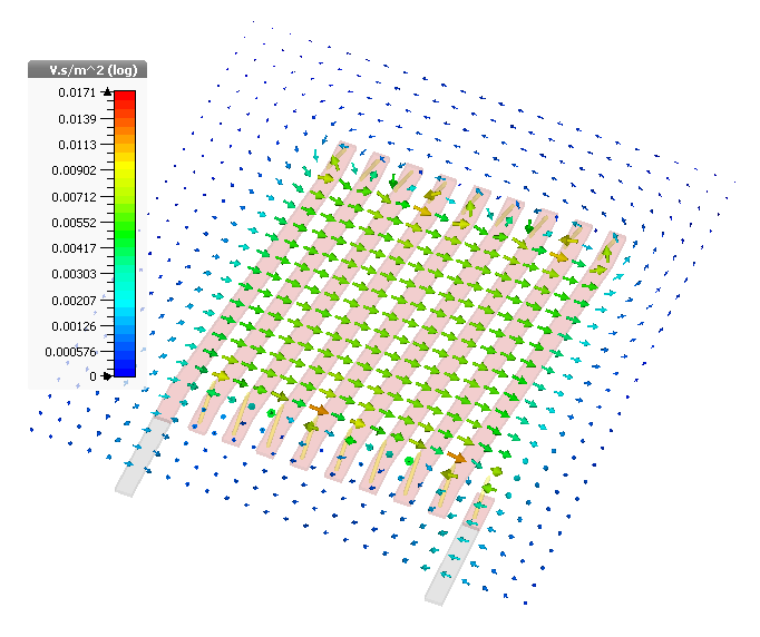
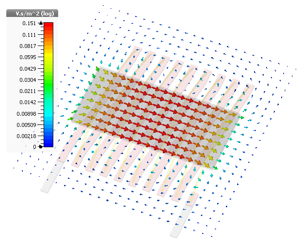
For the simulations, CST EM STUDIO was used to solve (1) and (2) and to compute the resistance and the inductance of the three different models. In the simulation of all considered models, electric boundary conditions were applied at a distance of from the model itself and a current of was applied as the excitation. To take into account the uncertainty in the core’s material parameters [11], a parameter sweep for model B was carried out to compute the inductance for the nominal and for the corner values of the core’s thickness. In Fig. 6, the results for model B are shown with respect to the relative permeability. Fixing the core’s thickness to a value of , a numerical optimization was applied to adjust the simulation model to the measurement results for model B. The optimization yielded a permeability of resulting in a simulated inductance of with a relative error of with respect to the measured value. With these values for the thickness and the permeability, model C and the transformer have been evaluated. To allow an assessment of the parasitic influences of the inductors, Fig. 7 shows the field plots for the magnetic flux density for models A and B.

| Model | in | in | in | in | in | in | in | |
|---|---|---|---|---|---|---|---|---|
| Model A | 23.74 | 23.77 | 0.13 | 1.08 | 0.89 | 17.59 | 4.63 | 62.11 |
| Model B | 147.26 | 147.42 | 0.11 | 1.12 | 0.89 | 20.54 | 6.23 | 11.27 |
| Model C | 347.27 | 1155.72 | 232.80 | 2.30 | 1.83 | 20.44 | 5.18 | 10.27 |
The results from measurement and simulation are summarized in Table II. The relative errors between measured and simulated resistances are all below . The remaining errors are assumed to stem mainly from the soldering joints that are not modeled in the simulation. While the relative errors of the inductance of models A and B are below , the simulated value for model C is much higher than the measured value. One possible reason for this deviation stems from non-idealities such as edges resulting from the laser cutting process. However, the major modeling error is assumed to result from a weak coupling within the sintered magnetic core due to a uniaxial anisotropy of the ferromagnetic foil, as also observed for sputtered ferrite cores in [13].
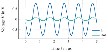
Despite the assumed weak coupling, a 1:1 transformer was successfully built. The measured input and output voltages for this transformer are shown in Fig. 8 giving a coupling factor of approximately at , whereas the simulated value for ideal isotropy is about .
Prototypes for on-chip inductors and transformers have been fabricated on printed circuit boards for cost-effective and reliable simulation models which enable system simulation for IC designers. Measurements of the air core inductor matched well with the simulation results. For inductances with closed magnetic core, the anisotropy of the material is assumed to be of great significance. This results in a very weak coupling of two inductors when placed on two opposite sides of a closed core. Nevertheless, the coupling is sufficient to allow the implementation of a transformer. Future work includes to investigate the error in the inductance of model C and the influence of the magnetic fields on any underlying ICs. Ultimately, design rules for the usage of bond wire inductors can be derived from the field results.
Acknowledgment
The authors thank Victoria Heinz, Isabel Kargar, David Riehl, and Timo Oster for their passionate work setting up the prototypes and simulation models. This work is supported by the Excellence Initiative of the German Federal and State Governments and the Graduate School CE at Technische Universität Darmstadt.
References
- [1] D. Dinulovic et al. High inductance thin-film transformer for high switching frequency. In 2018 IEEE Applied Power Electronics Conference and Exposition (APEC), pages 560–564, 2018. doi:10.1109/APEC.2018.8341067.
- [2] S. S. Mohan et al. Simple accurate expressions for planar spiral inductances. IEEE Journal of Solid-State Circuits, 34(10):1419–1424, 1999. doi:10.1109/4.792620.
- [3] J.-M. Yook et al. High-quality solenoid inductor using dielectric film for multichip modules. IEEE Transactions on Microwave Theory and Techniques, 53(6):2230–2234, 2005.
- [4] C. Ó. Mathúna et al. Review of integrated magnetics for power supply on chip (PwrSoC). IEEE Transactions on Power Electronics, 27(11):4799–4816, 2012. doi:10.1109/TPEL.2012.2198891.
- [5] D. Dinulovic et al. On-chip high performance magnetics for point-of-load high-frequency dc-dc converters. In 2016 IEEE Applied Power Electronics Conference and Exposition (APEC), pages 3097–3100, 2016. doi:10.1109/APEC.2016.7468306.
- [6] C. R. Sullivan et al. Integrating magnetics for on-chip power: A perspective. IEEE Transactions on Power Electronics, 28(9):4342–4353, 2013. doi:10.1109/TPEL.2013.2240465.
- [7] A. Camarda et al. Design and optimization techniques of over-chip bond-wire microtransformers with ltcc core. IEEE Journal of Emerging and Selected Topics in Power Electronics, 6(2):592–603, 2018.
- [8] E. Macrelli et al. Modeling, design, and fabrication of high-inductance bond wire microtransformers with toroidal ferrite core. IEEE Transactions on Power Electronics, 30(10):5724–5737, 2015.
- [9] Z. J. Shen et al. On-chip bondwire inductor with ferrite-epoxy coating: A cost-effective approach to realize power systems on chip. In 2007 IEEE Power Electronics Specialists Conference, pages 1599–1604, 2007. doi:10.1109/PESC.2007.4342235.
- [10] J. D. Jackson. Classical Electrodynamics Third Edition. Wiley, 1998.
- [11] Laird. MULL5040-200 Datasheet. (2019-09-05).
- [12] T. Brander. Trilogie der induktiven Bauelemente. Würth Elektronik, 4 edition, 2008.
- [13] J. M. Wright et al. Analysis of integrated solenoid inductor with closed magnetic core. IEEE Transactions on Magnetics, 46(6):2387–2390, 2010. doi:10.1109/TMAG.2010.2044982.