Assessing the role of interatomic position matrix elements in tight-binding calculations of optical properties
Julen Ibañez-Azpiroz1,2*, Fernando de Juan2,3, Ivo Souza1,2
1 Centro de Física de Materiales, Universidad del País Vasco, 20018 Donostia-San Sebastián, Spain
2 Ikerbasque Foundation, 48013 Bilbao, Spain
3 Donostia International Physics Center, 20018 Donostia-San Sebastián, Spain
* julen.ibanez@ehu.es
Abstract
We study the role of hopping matrix elements of the position operator in tight-binding calculations of linear and nonlinear optical properties of solids. Our analysis relies on a Wannier-interpolation scheme based on ab initio calculations, which automatically includes matrix elements of between different Wannier orbitals. A common approximation, both in empirical tight-binding and in Wannier-interpolation calculations, is to discard those matrix elements, in which case the optical response only depends on the on-site energies, Hamiltonian hoppings, and orbital centers. We find that interatomic -hopping terms make a sizeable contribution to the shift photocurrent in monolayer BC2N, a covalent acentric crystal. If a minimal basis of orbitals on the carbon atoms is used to model the band-edge response, even the dielectric function becomes strongly dependent on those terms.
1 Introduction
Empirical tight-binding (TB) is the method of choice for obtaining a simple and intuitive description of the electronic structure of solids [1]. In this method, the basis is defined implicitly through the on-site energies and the Hamiltonian hopping matrix elements,
| (1) |
without an explicit real-space representation of the basis orbitals.111As our focus will be on orthogonal TB models with Wannier functions (WFs) as basis orbitals, we adopt the notation that is widely used in the literature to denote the th Wannier orbital in the unit cell labeled by lattice vector . While that information is already sufficient to evaluate many physical quantities (energy bands, elastic constants, phonon spectra, etc.), the calculation of optical responses requires, in addition, the matrix elements of the position (dipole) operator in the TB basis.
In TB calculations of optical properties, it is customary to make the simplest possible approximation for the position matrix; namely, to discard all matrix elements of between different Wannier orbitals, which we will refer to as the “hopping matrix elements of ”, or simply “ hoppings.” When doing so, the only spatial information that is retained in the model are the orbital centers,
| (2) |
where is the center of the th Wannier orbital in the home cell. This minimal spatial embedding of a TB model already allows to incorporate electromagnetic fields in a gauge-invariant manner [2]. It is, nonetheless, a rather uncontrolled approximation: symmetry-allowed intra-atomic matrix elements such as are discarded along with interatomic matrix elements, all of which can in principle contribute to the optical response.
The above approximation has been discussed in the literature [3, 4, 5], and the general prescription for incorporating -hopping terms into both orthogonal [6] and non-orthogonal [7] TB models has been described. However, the impact of those terms on calculations of optical responses has not been thoroughly examined. An important step was taken in Refs. [4, 8], which examined the corrections from intra-atomic hoppings to the linear optical response of a toy model.
In this work, we revisit the problem from an ab initio perspective. We restore the hopping terms that are missing from Eq. (2),
| (3) |
and employ a first-principles-based WF method to assess their contribution to the linear and quadratic optical responses of a single layer of the graphitic material BC2N [9, 10, 11].
Our calculations use the Wannier interpolation method [6] and they proceed as follows. After performing an ab initio calculation of the electronic structure, we construct, in a post-processing step, well-localized WFs spanning the relevant bands. We then take those WFs and use them as an orthogonal TB basis to evaluate the band structure and the optical matrix elements. Since the Wannier orbitals are constructed explicitly, the hoppings can be tabulated and included, along with the on-site energies, orbital centers, and hoppings, in the calculation of optical responses; by selectively discarding some or all of the hoppings, we are able to gauge their contributions.
The optical responses analyzed in this work are the dielectric function and the shift photoconductivity. The latter is a quadratic response associated with a shift in the center of mass of an electron as it is optically excited from a valence band to a conduction band in a piezoelectric crystal [12, 13, 14], and is known to be quite sensitive to the spatial embedding of the TB model [15, 16]. (The same happens with the ground-state electric polarization [3], which is associated with the center of mass of valence electrons [17].)
Our test system, a single layer of BC2N, was chosen for the following reasons. (i) Its structure is noncentrosymmetric, a necessary condition for observing a quadratic response. (ii) As it is a covalent crystal with strong orbital overlap between different sites, interatomic terms can be expected to play a significant role. (iii) Its simple band structure near the fundamental gap allows for a complementary study based on a two-band model constructed from the Wannier Hamiltonian, which further highlights the impact of approximation (2).
The paper is organized as follows. In Sec. 2 we review the expressions for the dielectric function and shift photoconductivity in the independent-particle approximation. The connection between Wannier interpolation and TB theory, and the contribution of hoppings to the optical matrix elements, is discussed in Sec. 3. In Sec. 4 we describe the ab initio and Wannier-interpolation calculations, and in Sec. 5 we present and analyze the numerical results. We conclude in Sec. 6 with a summary and discussion, and in Appendix A we describe how the model is constructed.
2 Dielectric function and shift photoconductivity
In a nonmagnetic material such as BC2N, the dielectric function is a symmetric tensor whose imaginary part is absorptive, with an interband contribution given by [14]
| (4) |
Here is the elementary charge, and are differences between occupation factors and between band energies, in dimensions, and the integral is over the first Brillouin zone (BZ). Finally,
| (5) |
is the interband dipole given by the off-diagonal part of the Berry connection matrix
| (6) |
where denotes the cell-periodic part of a Bloch state .
Noncentrosymmetric crystals display a nonlinear optical effect known as the bulk photovoltaic (or photogalvanic) effect, which can be divided phenomenologically into “linear” and “circular” parts [18, 19, 20]. The linear bulk photovoltaic effect occurs in piezoelectric crystals such as BC2N, and is described by the relation
| (7) |
The shift current corresponds to the interband part of this response and is given by [14]
| (8) |
where
| (9) |
denotes the gauge-covariant “generalized derivative” of the interband dipole with respect to ( is the ordinary derivative).
3 Wannier interpolation
3.1 Energy bands
After the ab initio total-energy calculation, we construct in a post-processing step a set of well-localized WFs. These are chosen to span a group of bands that includes the initial and final states involved in interband absorption processes up to some desired frequency. From the Wannier orbitals we then define a set of Bloch basis states as
| (10) |
take matrix elements of the ab initio Hamiltonian between those states,
| (11) |
and diagonalize the resulting matrix,
| (12) |
With a proper choice of WFs, the eigenvalues provide a smooth interpolation across the BZ of the selected group of density functional theory (DFT) bands [21].
3.2 Optical matrix elements
The same interpolation strategy can be applied to other -space quantities. In particular, the transformed cell-periodic states
| (13) |
interpolate the ab initio cell-periodic eigenstates, allowing to treat wavefunction-derived quantities such as the Berry connection [6]. Inserting Eq. (13) in Eq. (6) yields
| (14a) | ||||
| (14b) | ||||
| (14c) | ||||
where
| (15) | |||||
and Eq. (3) was used in the last step. We will refer to and as the “internal” and “external” parts of the Berry connection matrix .222The generalized derivative of the interband dipole matrix [Eq. (9)] also splits into internal and external parts when expressed in the Wannier representation, see Ref. [22] for details.
The convention adopted in Eq. (10), with the phase factor included in the Bloch sum, is the most natural one for dealing with geometric quantities in space [23]. With that convention, when all hoppings are discarded Eq. (15) for vanishes identically so that reduces to the term given by [6]
| (16) |
where the numerator is an “effective” TB velocity matrix element obtained by substituting [2]. The term is “internal” in that it only depends on the minimal TB ingredients contained in Eqs. (1) and (2): on-site energies, (interatomic) hoppings, and Wannier centers.
Let us now restore the “external” -hopping terms, and examine their contributions to . Intra-atomic hoppings make a -independent contribution to Eq. (15), while the contribution from the interatomic ones varies with .333The distinction between intra- and inter-atomic hoppings can only be made when the Wannier orbitals are centered on the atoms, as is the case in the present study. In the limit where the overlap between orbitals on different sites is negligibly small, all interatomic terms vanish and Eq. (14) reduces to , where denotes the intra-atomic part of the -hopping matrix . Away from that limit, interatomic - and -hopping terms give competing contributions to .
Thus, the standard treatment of optical properties in TB can be systematically improved by progressively adding -hopping terms to the model in a sequence of steps:
-
1.
Only include on-site energies, orbital centers, and hoppings.
-
2.
Add intra-atomic hoppings (if any).
-
3.
Add nearest-neighbor interatomic hoppings.
-
4.
Add next-nearest-neighbor hoppings.
-
5.
…
Step 1 corresponds to the uncorrected TB model, step 2 adds the intra-atomic corrections, and steps 3 and higher incorporate interatomic corrections. Intra-atomic corrections are expected to be important for optical transitions involving localized orbitals [4]. The role of interatomic corrections remains less clear, as they were not considered in some of the previous works; they will be included below in our study of monolayer BC2N.
4 Structural and computational details
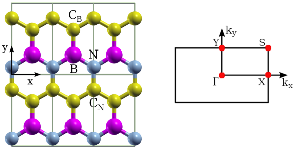
The structure of monolayer BC2N, depicted in Fig. 1, is formed by alternating zigzag chains of carbon and boron nitride atoms. The unit cell contains four atoms; the two carbon atoms are inequivalent, and we use the symbols CN and CB to label the ones with a nitrogen and a boron atom among their nearest neighbors (NNs), respectively. The structure is polar along , and has mirror symmetries and . The BZ is also shown in Fig. 1, with the high-symmetry points indicated.
The DFT calculations are performed using the Quantum ESPRESSO code package [24]. We treat the core-valence interaction using scalar-relativistic projector augmented-wave pseudopotentials taken from the Quantum ESPRESSO website. The pseudopotentials are generated with the Perdew-Burke-Ernzerhof exchange-correlation functional [25], and the energy cutoff for the plane-wave basis expansion is set at 70 Ry.
To study the monolayer we employ a slab of length 20 Å along the out-of-plane direction, and take the lattice constants ( Å along and Å along ) from Ref. [11]. For the self-consistent calculation we use a k-point mesh, and switch to a mesh for the non-self-consistent step from which we obtain the Bloch functions that are used as input for the Wannierization procedure [26, 21].
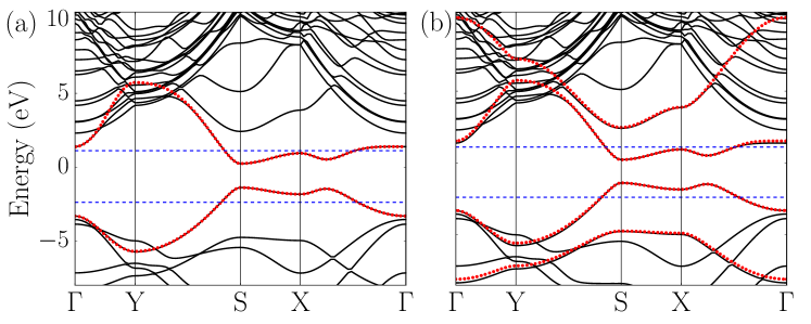
We use the Wannier90 code package [27] to generate atom-centered WFs spanning the states around the Fermi level. To that end, we employ a one-shot projection scheme [26] combined with band disentanglement [21]. We consider two different sets of WFs: one with a orbital on every atom (with an average quadratic spread of 1.08 Å2), and another with orbitals on the carbon atoms only (with an average spread of 3.39 Å2). The corresponding Wannier-interpolated bands are plotted in the two panels of Fig. 2 along with the DFT bands.
To obtain well-converged Wannier-interpolated spectra for the dielectric function and shift photoconductivity, we employ a dense k-point interpolation grid. We use a fixed width of 0.01 eV when broadening the delta functions in Eqs. (4) and (8), and apply a broadening of 0.04 eV to regularize the contribution of intermediate states to the shift current [22]. The occupation factors are evaluated at K.
5 Numerical results
5.1 Electronic structure and optical spectra
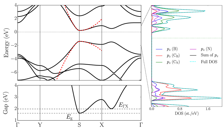
The DFT band structure of monolayer BC2N (black lines in Fig. 2) is replotted in Fig. 3 over a narrower energy range around the Fermi level, together with the direct gap and with the density of states (DOS) projected onto atomic orbitals. The minimum gap of eV occurs at the S point, and the electronic states near the band edge are composed almost entirely of orbitals, with only a small contribution from other orbitals – mainly – at higher energies (not shown). More precisely, the states at the top of the valence (bottom of the conduction) band are primarily composed of orbitals on the CB (CN) atoms, with smaller but non-negligible contributions from orbitals on the N and B atoms. These features guided our choice of the two Wannier basis sets described in Sec. 4. In particular, the larger set with one orbital on every atom captures the dominant orbital character at the band edge as well as the covalent nature of the system; we will use it in most of our calculations, with the exception of Sec. 5.3.1 where we switch to the minimal basis with orbitals on the carbon atoms only.
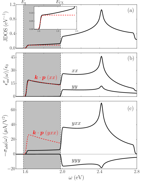
Next we analyze the optical response tensors evaluated by Wannier interpolation using our reference basis set. The symmetry-allowed components of the dielectric function are and , and those of the shift photoconductivity , , and ; for the sake of clarity, we focus on and . We report bulklike values for and , by rescaling the values obtained for the slab by a factor of ( Å is the slab thickness, and Å is the stacking distance) [16].
The joint density of states (JDOS) is shown in Fig. 4(a). It exhibits van Hove singularities at eV and eV, and a strong peak at 2.4 eV. These features carry over to the dielectric function in Fig. 4(b). Between and , is negligibly small; this is caused by mirror-parity selection rules [28] that are exact at and hold to a good approximation up to . Turning to the shift photoconductivity in Fig. 4(c), also peaks at eV while remains significantly smaller over the entire range shown. In the band-edge region, due to the same selection rules that enforce ; in contrast, is sizeable and shows a step-like feature followed by a plateau. Overall, the shapes of the and spectra are reminiscent of those of and , respectively.
5.2 Four-orbital tight-binding model
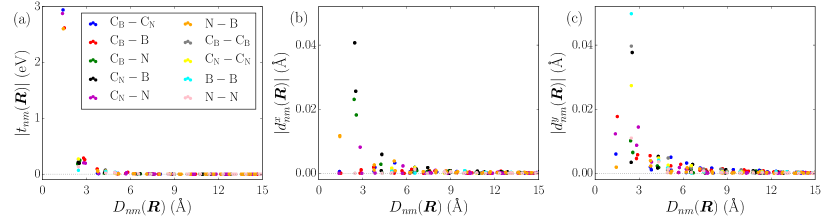
Since our Wannier basis contains one orbital per atom, the and hoppings in Eqs. (1) and (3) are purely interatomic. Their behavior as a function of distance
| (17) |
between orbitals is shown in Fig. 5. As expected from the localized nature of WFs, hoppings decay very rapidly with distance: the four NN hoppings at Å dominate over the rest by more than an order of magnitude, and hoppings beyond 3 Å are negligible. The behavior of and hoppings is more complex, with 1st NN coefficients being less than half the size of the dominant 2nd NN ones at Å. The largest coefficients overall are hoppings between boron pairs separated along , but hoppings as distant as Å remain sizeable. The longer range of hoppings compared to hoppings, as well as their non-monotonic behavior, seem reasonable given that the operator grows linearly with distance.
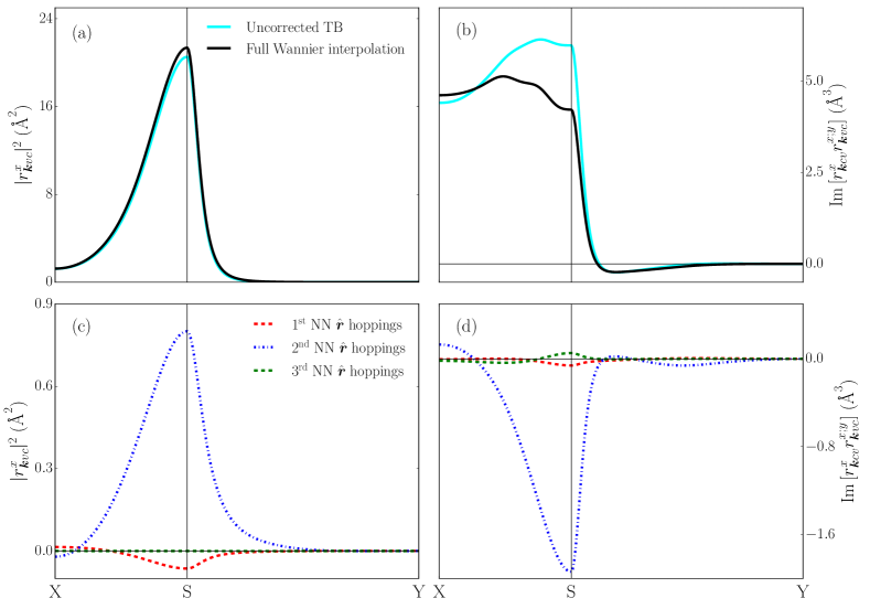
Let us now analyze the impact of hoppings on the calculated and spectra. Before coming to the full spectra, we first inspect the associated transition matrix elements between the top valence and bottom conduction bands. Their dispersions are plotted in Fig. 6; in panels (a,b) we compare full Wannier-interpolation results with uncorrected TB results obtained by setting all hoppings to zero, and in panels (c,d) we show the separate corrections to both matrix element from 1st and 2nd NN hoppings. The uncorrected TB approximation works very well for the matrix element: the largest relative error, which occurs around the band edge S, does not exceed 5%. That approximation is much less satisfactory for the matrix element, especially around S where the relative error reaches %. In the case of the matrix element, the small corrections to the TB approximation come mostly from 2nd NN hoppings; this is consistent with the behavior of those hoppings in Fig. 5(b), where 1st NN terms at Å are much smaller than 2nd NN ones at Å. The largest corrections to the matrix element again come from 2nd NN hoppings, as expected from Figs. 5(b,c) (the hoppings contribute through ).
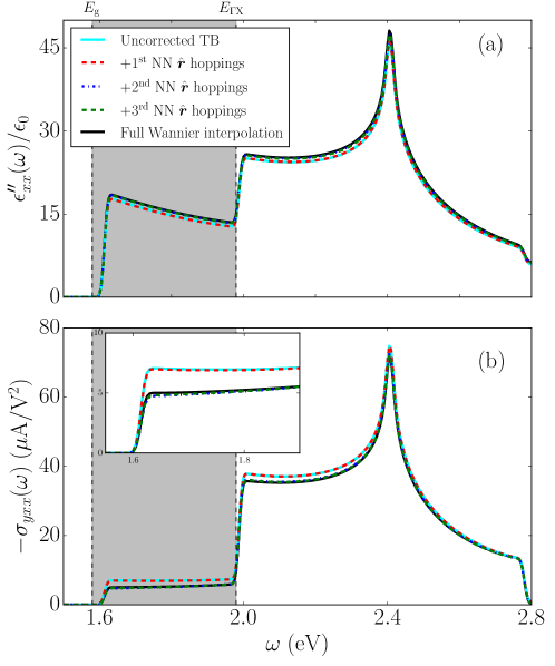
The full spectra and , calculated both with and without -hopping corrections, are displayed in Fig. 7. Consistent with the preceeding analysis, those corrections are fairly minor for , but they are significant for in the band-edge region, where hoppings up to 2nd NN have a sizeable impact on the computed spectrum.
5.3 Two-band models for the band edge

With the aim of reproducing the electronic and optical properties at the band edge in the simplest possible way, we now turn to minimal two-band models. We consider below two such models constructed in different ways.
5.3.1 Tight-binding model
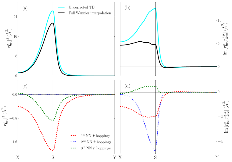
The first minimal model we consider is a TB model whose basis consists of -like WFs on the carbon atoms, forming a quasi one-dimensional chain along (see Fig. 1). As discussed in Sec. 4, this model is expected to yield acceptable results only at the band edge, where carbon states are prevalent.
The decay of the and hoppings in this model is shown in Fig. 8. Compared with the four-band model (Fig. 5), the decay is significantly slower. The largest hoppings have similar magnitudes in both models, while the largest and hoppings are an order of magnitude larger in the minimal model; as a result, hopping corrections are much more pronounced. This can be seen in the dispersions of the and matrix elements in Fig. 9: around S the corrections are significant already for [panels (a,c)], while in the case of [panels (b,d)] they reduce the matrix element by almost a factor of three, with the largest corrections coming from 1st and especially 2nd NN hoppings.
5.3.2 model
As an alternative approach for constructing a minimal band-edge model, we now extract a two-band effective Hamiltonian from our reference four-band TB Hamiltonian. This is motivated in part by previous works [16, 29, 30, 31], where two-band models were used to describe the band-edge photocurrent response of different types of materials.
Our model is constructed as described in Appendix A, by expanding the TB Hamiltonian (11) to second order in around the S point, and then applying Löwdin perturbation theory. The result is a transformed Hamiltonian , which we expand in terms of the identity matrix and of the Pauli matrices as
| (18) |
Its band dispersion in Fig. 3 agrees well with the DFT dispersion near the band edge.
Near the band edge, the dielectric function and shift photoconductivity are given by the product between the transition matrix elements and the JDOS [16],
| (19) | |||
| (20) |
The expressions for the matrix elements at a band extremum read [16, 32]
| (21) |
and
| (22) |
where the coefficients , , and are evaluated at the S point using Eq. (32) in Appendix A, and is the Levi-Civita symbol. Note that these expressions only depend on the Hamiltonian, which in turn is constructed from the TB Hamiltonian; thus, hoppings are not taken into account when evaluating optical matrix elements from a TB-derived model.
The results for the JDOS, , and are shown as dashed red lines in the shaded regions of Fig. 4. Panel (a) shows a good agreement with the Wannier-interpolated JDOS around the band gap: the height of the step-like feature at is nicely reproduced, and although the Wannier-interpolation curve grows monotonically above while the one stays flat, the discrepancy is small. In panel (b), the curve for matches very well the Wannier-interpolation one over the entire band-edge region: it reproduces not only the step height at but also the subsequent decrease, thanks to the factor in Eq. (21). In contrast, in panel (c) the curve for deviates considerably from the Wannier-interpolation one, overshooting it by about a factor of five at . This is in line with our previous finding that the matrix element at the S point gets strongly reduced when hopping terms are included.
6 Discussion
The question of how to evaluate optical matrix elements was debated in the TB literature until the early 2000s (see Ref. [4] for an overview). It eventually became clear that the “minimal TB substitution” for the velocity matrix elements leaves out important physics. In particular, it completely neglects intra-atomic dipole transitions [4], as well as corrections to interatomic transitions from off-site dipole matrix elements. Although the shortcomings of the minimal (or uncorrected) TB approach to the calculation of optical matrix elements are by now well understood, that approach continues to be widely used because it requires no additional parameters beyond the standard ones: on-site energies, hoppings, and orbital centers.
The development of Wannier-interpolation schemes by the ab initio electronic-structure community provided an opportunity to assess the importance of those additional TB parameters (hopping matrix elements of ) to various transport and optical responses in a wide range of materials. In the early works on Wannier interpolation [6, 33], the anomalous Hall conductivity and magnetic circular dichroism spectrum of bcc Fe were found to be very well described by the uncorrected TB approach where all hopping terms are discarded.
More recently, Wannier interpolation has been used to calculate nonlinear optical responses, and more pronounced -hopping corrections were found in some cases, such as the shift photoconductivities of WS2 [34] and especially GaAs [22], and the high-harmonic generation spectrum of monolayer hexagonal BN [35]. This provided the motivation for the present work, where we carried out a systematic study of the impact of hopping matrix elements of on the linear (dielectric function) and quadratic (shift photoconductivity) optical responses of monolayer BC2N.
Our findings can be summarized as follows: (i) hoppings decay more slowly with distance than hoppings, and 2nd NN hoppings can be significantly larger than 1st NN ones; (ii) hoppings are more important for the shift current than for the dielectric function, indicating that the former is more sensitive to the spatial structure of the WFs; (iii) the importance of -hopping corrections increases as the number of Wannier basis orbitals decreases, since the Wannier orbitals tend to be more extended in minimal bases; (iv) two-band Hamiltonians constructed from TB Hamiltonians are likely to provide a poor description of the shift-current response at the band edge, due to the neglect of -hopping corrections.
Despite being available “for free” within the Wannier interpolation framework, hoppings are often discarded in Wannier-based calculations of nonlinear optical responses (for some recent examples, see Refs. [36, 37, 38, 31]). Our results indicate that this common practice is ill-advised, since the error incurred can sometimes be significant.
One question that the present work does not address, and which could be an interesting direction for future research, is how to devise reasonable approximations for the hopping matrix elements of in the context of empirical TB theory, where the basis orbitals are not explicitly available.
Acknowledgements – We thank David Vanderbilt, Michele Modugno and Stepan Tsirkin for discussions. This work was supported by Grant No. FIS2016-77188-P from the Spanish Ministerio de Economía y Competitividad. This project has also received funding from the European Union’s Horizon 2020 research and innovation programme under the Marie Sklodowska-Curie grant agreement No 839237 and the European Research Council (ERC) grant agreement No 946629.
Appendix A Construction of the model
Our model is obtained by first carrying out a series expansion of the four-band TB Hamiltonian around the S point, and then using the Löwdin partitioning scheme to reduce it to a two-band Hamiltonian. This is a standard procedure for constructing models starting from TB Hamiltonians [39, 40], and here we describe our Wannier-based implementation.
A.1 Löwdin partitioning
We begin by reviewing the Löwdin parititioning scheme [41]. Consider a Hamiltonian
| (23) |
where the eigenvalues and eigenfunctions of are known, and is a perturbation. Quasi-degenerate (Löwdin) perturbation theory assumes that the set of eigenfunctions of can be divided into subsets A and B that are weakly coupled by , and that we are only interested in subset A, the “active” subspace. This theory asserts that a transformed Hamiltonian exists within subspace A such that
| (24) |
where contain matrix elements of to the th power. The first three terms are [41]
| (25) | |||
| (26) | |||
| (27) |
where and . The approximation amounts to truncating to the A subspace. By adding , the coupling to the B subspace is taken into account.
A.2 From tight-binding to
We shift the origin of space to a reference point (the S point, in our application), and Taylor expand the Wannier Hamiltonian (11) up to second order in ,
| (28) |
(the notation for derivatives is the same as in Eq. (22)). Applying to Eq. (28) a similarity transformation that diagonalizes the -independent term, we obtain the transformed Hamiltonian
| (29) |
where we introduced the notation , and applied it to . Next we apply Löwdin partitioning, choosing the diagonal matrix as the of Eq. (23), and the remaining terms in Eq. (29) as . Collecting terms in Eq. (24) we get
| (30) |
where
| (31) |
and . These equations define the effective Hamiltonian in the A sector.
Since in our application the A sector contains two bands, we expand the Hamiltonian as in Eq. (18) in the main text. To evaluate Eqs. (21) and (22) in the main text, we need the quantities , , and at the reference point. Inserting Eq. (30) in the expression , we find
| (32a) | ||||
| (32b) | ||||
| (32c) | ||||
where the traces involve the A-sector blocks of the matrices , , and .
References
- [1] W. A. Harrison, Electronic Structure and the Properties of Solids, Freeman, San Francisco (1980).
- [2] M. Graf and P. Vogl, Electromagnetic fields and dielectric response in empirical tight-binding theory, Phys. Rev. B 51, 4940 (1995), 10.1103/PhysRevB.51.4940.
- [3] J. Bennetto and D. Vanderbilt, Semiconductor effective charges from tight-binding theory, Phys. Rev. B 53, 15417 (1996), 10.1103/PhysRevB.53.15417.
- [4] T. G. Pedersen, K. Pedersen and T. Brun Kriestensen, Optical matrix elements in tight-binding calculations, Phys. Rev. B 63, 201101 (2001), 10.1103/PhysRevB.63.201101.
- [5] B. A. Foreman, Consequences of local gauge symmetry in empirical tight-binding theory, Phys. Rev. B 66, 165212 (2002), 10.1103/PhysRevB.66.165212.
- [6] X. Wang, J. R. Yates, I. Souza and D. Vanderbilt, Ab initio calculation of the anomalous Hall conductivity by Wannier interpolation, Phys. Rev. B 74, 195118 (2006), 10.1103/PhysRevB.74.195118.
- [7] C.-C. Lee, Y.-T. Lee, M. Fukuda and T. Ozaki, Tight-binding calculations of optical matrix elements for conductivity using nonorthogonal atomic orbitals: Anomalous Hall conductivity in bcc Fe, Phys. Rev. B 98, 115115 (2018), 10.1103/PhysRevB.98.115115.
- [8] T. Sandu, Optical matrix elements in tight-binding models with overlap, Phys. Rev. B 72, 125105 (2005), 10.1103/PhysRevB.72.125105.
- [9] A. Y. Liu, R. M. Wentzcovitch and M. L. Cohen, Atomic arrangement and electronic structure of N, Phys. Rev. B 39, 1760 (1989), 10.1103/PhysRevB.39.1760.
- [10] M. Watanabe, S. Itoh, K. Mizushima and T. Sasaki, Electrical properties of BC2N thin films prepared by chemical vapor deposition, J. Appl. Phys. 78, 2880 (1995), https://doi.org/10.1063/1.360029.
- [11] Z. Pan, H. Sun and C. Chen, Interlayer stacking and nature of the electronic band gap in graphitic : First-principles pseudopotential calculations, Phys. Rev. B 73, 193304 (2006), 10.1103/PhysRevB.73.193304.
- [12] R. von Baltz and W. Kraut, Theory of the bulk photovoltaic effect in pure crystals, Phys. Rev. B 23, 5590 (1981), 10.1103/PhysRevB.23.5590.
- [13] V. I. Belinicher, E. L. Ivchenko and B. I. Sturman, Hall effect for bulk photovoltaic current in the piezoelectric ZnS, Sov. Phys. JETP 56, 359 (1982).
- [14] J. E. Sipe and A. I. Shkrebtii, Second-order optical response in semiconductors, Phys. Rev. B 61, 5337 (2000), 10.1103/PhysRevB.61.5337.
- [15] H. Presting and R. Von Baltz, Bulk Photovoltaic Effect in a Ferroelectric Crystal: A Model Calculation, Phys. Status Solidi (b) 112, 559 (1982), 10.1002/pssb.2221120225.
- [16] A. M. Cook, B. M. Fregoso, F. d. Juan, S. Coh and J. E. Moore, Design principles for shift current photovoltaics, Nat. Commun. 8, 14176 (2017), 10.1038/ncomms14176.
- [17] R. D. King-Smith and D. Vanderbilt, Theory of polarization of crystalline solids, Phys. Rev. B 47, 1651 (1993), 10.1103/PhysRevB.47.1651.
- [18] V. I. Belinicher and B. I. Sturman, The photogalvanic effect in media lacking a center of symmetry, Soviet Physics Uspekhi 23(3), 199 (1980), 10.1070/PU1980v023n03ABEH004703.
- [19] B. I. Sturman and V. M. Fridkin, The photovoltaic and photorefractive effects in noncentrosymmetric materials, Gordon and Breach, ISBN 978-2-88124-498-8 (1992).
- [20] E. L. Ivchenko and G. E. Pikus, Superlattices and Other Heterostructures, Springer, Berlin, 10.1007/978-3-642-60650-2 (1997).
- [21] I. Souza, N. Marzari and D. Vanderbilt, Maximally localized Wannier functions for entangled energy bands, Phys. Rev. B 65, 035109 (2001), 10.1103/PhysRevB.65.035109.
- [22] J. Ibañez-Azpiroz, S. S. Tsirkin and I. Souza, Ab initio calculation of the shift photocurrent by Wannier interpolation, Phys. Rev. B 97, 245143 (2018), 10.1103/PhysRevB.97.245143.
- [23] D. Vanderbilt, Berry Phases in Electronic Structure Theory: Electric Polarization, Orbital Magnetization and Topological Insulators, Cambridge University Press, Cambridge (United Kingdom), 10.1017/9781316662205 (2018).
- [24] P. Giannozzi, S. Baroni, N. Bonini, M. Calandra, R. Car, C. Cavazzoni, D. Ceresoli, G. L. Chiarotti, M. Cococcioni, I. Dabo, A. D. Corso, S. de Gironcoli et al., QUANTUM ESPRESSO: a modular and open-source software project for quantum simulations of materials, J. Phys.: Condens. Matter 21, 395502 (2009), 10.1088/0953-8984/21/39/395502.
- [25] J. P. Perdew, K. Burke and M. Ernzerhof, Generalized Gradient Approximation Made Simple, Phys. Rev. Lett. 77, 3865 (1996), 10.1103/PhysRevLett.77.3865.
- [26] N. Marzari and D. Vanderbilt, Maximally localized generalized Wannier functions for composite energy bands, Phys. Rev. B 56, 12847 (1997), 10.1103/PhysRevB.56.12847.
- [27] G. Pizzi, V. Vitale, R. Arita, S. Blügel, F. Freimuth, G. Géranton, M. Gibertini, D. Gresch, C. Johnson, T. Koretsune, J. Ibañez-Azpiroz, H. Lee et al., Wannier90 as a community code: new features and applications, Journal of Physics: Condensed Matter (2019), 10.1088/1361-648X/ab51ff.
- [28] J. Ibañez-Azpiroz, I. Souza and F. de Juan, Directional shift current in mirror-symmetric , Phys. Rev. Research 2, 013263 (2020), 10.1103/PhysRevResearch.2.013263.
- [29] Z. Yan, Precise determination of critical points of topological phase transitions via shift current in two-dimensional inversion asymmetric insulators, arXiv:1812.02191 [cond-mat] (2018-12-05), 1812.02191.
- [30] J. Ahn, G.-Y. Guo and N. Nagaosa, Low-Frequency Divergence and Quantum Geometry of the Bulk Photovoltaic Effect in Topological Semimetals, Phys. Rev. X 10, 041041 (2020), 10.1103/PhysRevX.10.041041.
- [31] H. Xu, H. Wang, J. Zhou, Y. Guo, J. Kong and J. Li, Colossal switchable photocurrents in topological janus transition metal dichalcogenides, npj Comput Mater 7(1), 1 (2021), 10.1038/s41524-021-00499-4.
- [32] A. Bácsi and A. Virosztek, Low-frequency optical conductivity in graphene and in other scale-invariant two-band systems, Phys. Rev. B 87, 125425 (2013), 10.1103/PhysRevB.87.125425.
- [33] J. R. Yates, X. Wang, D. Vanderbilt and I. Souza, Spectral and Fermi surface properties from Wannier interpolation, Phys. Rev. B 75, 195121 (2007), 10.1103/PhysRevB.75.195121.
- [34] C. Wang, X. Liu, L. Kang, B.-L. Gu, Y. Xu and W. Duan, First-principles calculation of nonlinear optical responses by Wannier interpolation, Phys. Rev. B 96, 115147 (2017), 10.1103/PhysRevB.96.115147.
- [35] R. E. F. Silva, F. Martín and M. Ivanov, High harmonic generation in crystals using maximally localized Wannier functions, Phys. Rev. B 100, 195201 (2019), 10.1103/PhysRevB.100.195201.
- [36] Y. Zhang, F. de Juan, A. G. Grushin, C. Felser and Y. Sun, Strong bulk photovoltaic effect in chiral crystals in the visible spectrum, Phys. Rev. B 100, 245206 (2019), 10.1103/PhysRevB.100.245206.
- [37] Y. Zhang, H. Ishizuka, J. van den Brink, C. Felser, B. Yan and N. Nagaosa, Photogalvanic effect in Weyl semimetals from first principles, Phys. Rev. B 97, 241118 (2018), 10.1103/PhysRevB.97.241118.
- [38] B. Sadhukhan, Y. Zhang, R. Ray and J. van den Brink, First-principles calculation of shift current in chalcopyrite semiconductor , Phys. Rev. Materials 4, 064602 (2020), 10.1103/PhysRevMaterials.4.064602.
- [39] G.-B. Liu, W.-Y. Shan, Y. Yao, W. Yao and D. Xiao, Three-band tight-binding model for monolayers of group-VIB transition metal dichalcogenides, Phys. Rev. B 88, 085433 (2013), 10.1103/PhysRevB.88.085433.
- [40] S. Fang, R. Kuate Defo, S. N. Shirodkar, S. Lieu, G. A. Tritsaris and E. Kaxiras, Ab initio tight-binding Hamiltonian for transition metal dichalcogenides, Phys. Rev. B 92, 205108 (2015), 10.1103/PhysRevB.92.205108.
- [41] R. Winkler, Spin-orbit Coupling Effects in Two-Dimensional Electron and Hole Systems, Springer, 2003 edition edn., ISBN 978-3-540-01187-3 (2003).