Purcell-Enhanced Emission from Individual SiV- Center in Nanodiamonds Coupled to a Si3N4-Based, Photonic Crystal Cavity
Abstract
Hybrid quantum photonics combines classical photonics with quantum emitters in a postprocessing step. It facilitates to link ideal quantum light sources to optimized photonic platforms. Optical cavities enable to harness the Purcell-effect boosting the device efficiency. Here, we postprocess a free-standing, crossed-waveguide photonic crystal cavity based on Si3N4 with SiV- center in nanodiamonds. We develop a routine that holds the capability to optimize all degrees of freedom of the evanescent coupling term utilizing AFM nanomanipulation. After a few optimization cycles we resolve the fine-structure of individual SiV- centers and achieve a Purcell enhancement of more than 4 on individual optical transitions, meaning that four out of five spontaneously emitted photons are channeled into the photonic device. Our work opens up new avenues to construct efficient quantum photonic devices.
I Introduction
Diamond is among the leading material platforms for spin-based photonic quantum technologies Atatüre et al. (2018); Awschalom et al. (2018).
The negatively-charged silicon-vacancy center (SiV- center) became one of the most promising color center in diamond due to strong zero phonon line (ZPL) emission, narrow inhomogeneous distribution and negligible spectral diffusion
Becker and Becher (2017); Rogers et al. (2019)
enabling two-photon interference from distinct SiV- centers without the need of frequency tuning Sipahigil et al. (2014). The electronic spin coherence is limited by rapid phonon-mediated relaxation but can be improved by applying high strain Sohn et al. (2018) or by suppressing phonon-mediated relaxation at milli Kelvin temperatures Sukachev et al. (2017). Recently, the deterministic polarisation of a small nuclear spin ensemble via dynamic nuclear polarization was demonstrated Metsch et al. (2019).
Integrating the SiV- center into on-chip photonics enables efficient spin-photon interface by Purcell-enhancement and scalable photonic networks. Classical fabrication methods for photonics platforms based on materials such as GaP, Si or Si3N4 show low photon loss, design fexibility, standardization of the fabrication process, high throughput production or scalability to large-scale designs. It is therefore desirable to functionalize classical photonics for quantum applications.
Hybrid approaches pick up that challenge by combining quantum emitters with the most suitable photonics platforms. The post-processing step is an extraordinary challenge and can, for example, be realized by evanescent coupling. An idealized procedure utilizes preselected quantum emitters in a nanometersized host matrix to position the quantum light source with high accuracy in the interaction zone of the photonic device. Hybrid attempts based on color centers in diamond and high-refractive index photonics devices have been demonstrated in the past years
Fu et al. (2008); Englund et al. (2010); Barclay et al. (2011); Wolters et al. (2010)
with challenges arising from weak evanescent coupling, high-background fluorescence or -factor degradation Radulaski et al. (2019). Reasonably large coupling was achieved between an ensemble of center in nanodiamonds (NDs) and the mode of a high-, free-standing photonic crystal cavity (PCC) in Si3N4 where, at the same time, the background fluorescence was suppressed by
in a crossed-waveguide pump-probe design Fehler et al. (2019).
In this work we post-process a high- photonic crystal cavity (PCC) based on Si3N4 which was optimized for quantum photonics applications with SiV- centers in NDs. We take advantage of bulk-like optical and coherence properties of SiV-center in nanodiamonds Jantzen et al. (2016); Häußler et al. (2019), and high-precision nanomanipulation
tools Schell et al. (2011); Rogers et al. (2019) in order to access all degrees of freedom of the coupling term to the SiV-center Häußler et al. (2019). After a few optimization cycles on the evanescent coupling term we achieve a coherent coupling of the zero-phonon line (ZPL) to the mode of the PCC with a -factor of 0.44 and a Purcell factor of 0.79 averaged over an ensemble of SiV- centers. After cooling the sample to liquid Helium temperatures we resolve the fine-structure of individual SiV- centers and achieve a Purcell enhancement of more than 4 for individual optical transitions. The highly efficient coupling of individual atomic transitions to photonic circuits lays the foundation for quantum applications such as quantum networks Wehner et al. (2018) or on-chip Boson sampling Spring et al. (2013); Li et al. (2016); Zhou et al. (2017) based on hybrid quantum photonics.
II Results
Photonic Crystal Cavity
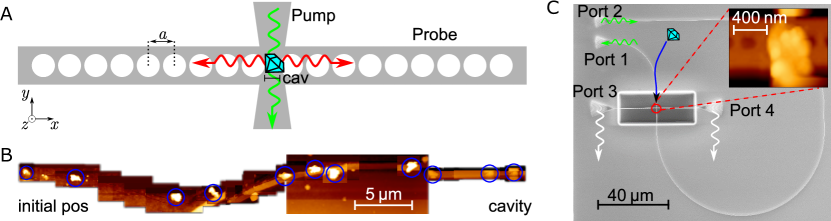
Our platform consists of a free-standing, crossed-waveguide PCC in Si3N4 featuring low-loss transmission and high-mode confinement together with a minimized cross-talk between pump and probe waveguide ( ). On-chip, off-resonant excitation and emission is spatially separated. While the pump waveguide is optimized for , the probe waveguide is optimized for , which matches the ZPL of the SiV- center. Both waveguides are connected to grating couplers, which allow for out-of-plane excitation and readout. The on-chip excitation of the SiV- centers is achieved by evanescent coupling to the pump waveguide. The probe waveguide hosts a 1D photonic crystal cavity with its modes superimposed to the pump volume. Each cavity mirror consist of holes with a period of . This periodic variation of permittivity forms a band gap in the visible range. A distance between these two mirrors is inserted, which results in spectrally separated states inside the photonic band gap optimized by FDTD simulations. The nanophotonic circuit is post-processed with an SiV- ensemble inside the crossing area of pump and probe beam (interaction zone), which is sketched in Fig. 1 A.
Post-Processing
The post-processing step for placing the ND within the interaction zone of the PCC follows the procedure described in Reference Schell et al. (2011); Fehler et al. (2019).
A dispersion of NDs in water with incorporated SiV- color centers is coated on the surface of the PCC chip. Suitable SiV- center are preselected using a custom-build confocal microscope. Superimposing the confocal scan with an AFM image enables the precise localization of the SiV- center host crystal. After the preselected ND is found, the AFM cantilever tip is used to push the ND in the interaction zone of the PCC.
Several steps of the positioning procedure are shown in Fig. 1 B. The ND is pushed along a total distance of over .
The manipulation path is schematically drawn in the SEM image of the photonic device in Fig. 1 C. The positioned ND is off-resonantly excited through port 1 and its emission into the cavity-waveguide can be read out at port 3 and 4. The small inset shows an AFM image of the positioned ND in the interaction zone.
A cross-talk measurement of the empty PCC probes the resonance modes. Therefore, a laser with is coupled into port 1 and the cavity signal is collected at port 3. The signal, arising from Si3N4 background fluorescence, is shown in Fig 3 A (green). The occurring peaks correspond to the respective cavity modes, where the highest resonance at shows a quality factor of and the resonance near has a -factor of .
Simulation of LDOS
The design of the freestanding PCC is numerically optimized via 3D FDTD simulations Oskooi et al. (2010). The PCC consists of two modulated Bragg mirrors with inserted cavity region in between. The periodicity of the holes () is determined to match the bandgap region of the PCC to the investigated wavelength of the SiV- ZPL. To achieve high -factors optimization on the cavity length and hole diameter was performed Fehler et al. (2019); Akahane et al. (2003).
For a maximum enhancement of the emitted light, the source need to be placed in the antinode of the electric field distribution of the resonance mode Purcell et al. (1946). Thus, the position of the SiV- embedded in a ND is carried out via 3D FDTD simulations Oskooi et al. (2010) in two steps. For the simulation a cube-shaped () ND is placed on the cavity region.
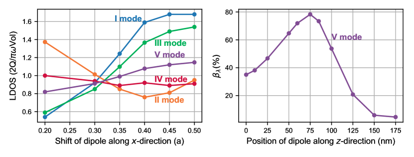
The coupling strength between the optical dipole transition and the cavity field mode depends, in particular, on the dipole orientation and the position with respect to the cavity field. Both parameters can be accessed by nanomanipulation as demonstrated in reference Häußler et al. (2019) without altering the optical properties of the SiV- center. While the dipole orientation shows a cosine dependence the dipole position requires a more sophisticated study. The first optimization step is the enhancement of the Local Density of States (LDOS) dependent on the emitter position (see Fig. 2 A). The LDOS is proportional to the overlap integral between the electric field distribution of the resonance mode and the emitter Taflove et al. (2013). According to the axes in Fig. 1 A the dipole position, embedded in a ND placed on the cavity, is centered along - and -direction and varied along the longitudinal -direction, since this component shows the strongest contribution to the convolution. The rotational orientation of the dipole is aligned to the PCC axis for highest coupling. The overlap integral of the dipole and the electric field follows a cosine dependence and is therefore one for the aligned case and zero for the orthogonal orientation. The normalized LDOS enhancement is calculated for each position of the dipole with respect to the field distribution of the mode. Therefore, the enhancement of the LDOS through the cavity is divided by the LDOS enhancement for a waveguide without cavity. The highest enhancement (see Fig. 2A) for odd modes is achieved for a dipole shift of (0.4-0.45) from the symmetry plane of the center of the cavity, matching an antinode of the electric field distribution. For a reduction in simulation time, the number of segments in each Bragg-mirror was reduced to , since the electric field distribution (position of minimum and maximum) of resonance modes changes in a minor way with varying number of segments.
The second part of the 3D FDTD simulations targeted the position optimization of the ND embedded emitter along the -axis. Therefore, we quantify the coupling of the emitter to the cavity with the -factor Fehler et al. (2019), which gives the ratio of coupled spontaneous emission and the total amount of spontaneously emitted photons to free space and in the cavity :
| (1) |
The -factor (spectrally resolved -factor Fehler et al. (2019)), correlating with LDOS enhancement, of the emission into the researched V-order resonance mode was examined. To consider the experimental degradation of the PCC due to the presence of the ND in the simulation, the number of segments in each Bragg-mirror was reduced. For this purpose, the number of holes is gradually adjusted from to 27 until the simulated -factor matches the experimentally examined -factor. The center of the ND was shifted according the to the position in the AFM image in Fig 1 C. The -position of the dipole inside the ND is set to its optimal according to Fig. 2 A, while the -distance from the surface of the cavity is altered. The resulting coupling efficiencies for different -positions are shown in Fig. 2 B. The maximum value of is reached for the source being located above the surface of the cavity.
FDTD simulations are carried out to compute the Purcell enhancement Purcell et al. (1946) for the Vth-order resonance mode of the cross-bar PCCs with and holes, each with a cube-shaped ND crystal on the cavity region as described above. The resulting Purcell-factors read and , respectively for a spectrally and polarization matched resonance mode and an emitter located at the antinode of the electric field.
Purcell-Enhanced Photon Emission
After the ND is positioned on top of the interaction zone, the sample is placed inside a flow-cryostat and cooled to approximately . The emitter-cavity system is excited via port 1 with of green laser while the emission is collected through port 3 (shown in Fig. 3 A in orange). In blue, the free space emission of the SiV- center is shown, where the ensemble is evanescently excited through port 1 and the emission is collected at the center position of the ND. Both collection procedures are shown in the small insets in Fig. 3 A.
The presence of the ND in the interaction zone changes the effective refractive index of the cavity. This leads to a red shift of the desired cavity resonance. Together with a change in temperature the shift is approximately . The altered mode at of the PCC is fed by the ZPL of the SiV- ensemble. The other resonances are slightly enhanced due to phonon side band coupling and scattered background fluorescence. The -factor of the desired resonance decreased from for the empty cavity to for the coupled system caused by scattering losses and degradation of the PCC.
According to equation (1), we obtain a coupling of:
| (2) |
where is the coupler efficiency and is the collection efficiency of the free space emission. The coupler efficiency is determined via a transmission measurement of a laser at the desired wavelength through the probe beam. The free space collection efficiency is limited due to a NA=0.55 objective. Please note, that the dipole alignment of the SiV- center is such that high free-space emission corresponds to the best coupled SiV- centers, while our geometry does not allow for artificially decreased ratio between free-space and waveguide emission. The achieved -factor corresponds to nearly every second photon being emitted into the cavity resonance and leads to an average Purcell-enhancement Zhang et al. (2018) of
| (3) |
for all emitters inside the SiV- ensemble.
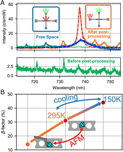
The tuning mechanisms for modifying the ensemble coupling utilized so far, are position of the ND and temperature. In Fig. 3 B the -factors after optimizing the position of the ND and after temperature tuning are shown. The position and orientation of the ND in the interaction zone can be controlled by AFM-based nanomanipulation
Häußler et al. (2019),
which yields to a better dipole alignment of the ND to the cavity axis. Position 1 and position 2 in Fig. 3 B correspond to a coupling averaged over the whole ensemble of 0.14 and 0.31, respectively. At position 2 we cooled the sample from to . This further increased the average ensemble -factor to 0.44 (as shown in Fig. 3 A and given in equation (1)).
Additional reduction of the temperature to reveals the fine structure splitting of the SiV- centers in the ensemble. Thus, instead of the average ensemble coupling the -factors of individual transitions of single SiV- centers can be determined, as depicted in Fig. 4. Again, the free space emission (blue) needs to be compared to the joint emitter cavity signal (insets Fig. 3 A). Freezing and unfreezing processes, together with temperature tuning further shifted the central frequency of the resonance mode to approximately (depicted in gray Fig. 4 top). This implies a detuning from the average ensemble ZPL resonance at leading to decreased average coupling. The detuning enables the coupling of individual, however more strained, SiV- centers (Fig. 4 top), apparent when zooming into the red square (Fig. 4 bottom). A splitting of between the doublet of (A,B) and (C,D) is observed, while the splitting between C and D is . These four lines arise from one SiV- center with an excited state splitting of and a ground state splitting of influenced by the strain inside the ND Rogers et al. (2019), where the ZPL position of the SiV- can be shifted (axial strain) while keeping the state splitting constant (low transverse strain)Meesala et al. (2018). The used NDs have proven to inhere low transverse strain Rogers et al. (2019). For the SiV- center transition A and D have the same dipole orientation as well as transition B and C Rogers et al. (2014). Fig. 4 confirms that transition B and C show a better coupling to the cavity mode than transition A and D originating from dipole alignment of the emitter to the cavity axis. Due to strain induced differences in the selection rules, transition B and C show different enhancement factors Hepp et al. (2014).
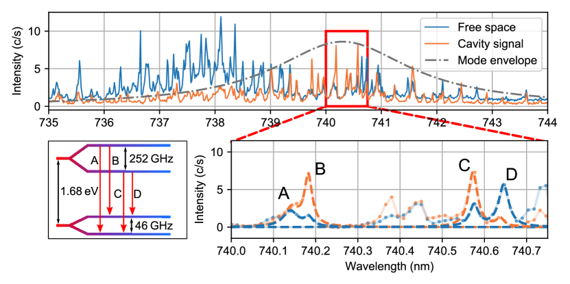
Similar dipole orientation of the transitions reach higher (B and C) and lower (A and D) coupling efficiencies to the cavity mode. From these values according to equation (1), we estimate the -factor for all four transitions. The highest coupling was achieved for transition B, which is . This value translates to a Purcell enhancement of
4/5 of the total spontaneous emission are channeled into the photonic circuit. The measured -factor of corresponds to a lifetime reduction of , where is the lifetime of the SiV- without cavity. The resulting lifetime for the SiV- on resonance with the cavity is about ps, too short to be observed with our current experimental equipment.
Outlook
In our work we demonstrate the efficient coupling of individual optical transitions of SiV- centers to a Si3N4-based cross-bar PCC with a Purcell enhancement of more than 4, where the enhanced signal was read out via a probe waveguide (with a PCC) by excitation via a crossed waveguide on chip. Much higher Purcell enhancement is prohibited by residual scattering from the ND reducing the overall Q-factor of the PCC. Furthermore, the achievable evanescent coupling strength is ultimately limited by the distance of the SiV- center to the field maximum of the PCC. In future experiments we envision Purcell factors beyond 100 for single SiV- center in nanodiamonds with diameter of a few ten nanometers. To emphasize the influence of the ND emitter host on the Purcell enhancement factor simulations without the scattering crystal were computed leading to (; ) and (; ), respectively for matched polarization of the emitter-cavity systems. For the first time, we experimentally demonstrate Purcell enhancement well above one for hybrid quantum photonics with SiV center in NDs matching recently simulated Purcell factors of Radulaski et al. (2019). In agreement with our simulations, Purcell factors of more than 500 were envisioned for less-degraded systems Radulaski et al. (2019). The investigated hybrid quantum photonics platform brings cavity-mediated entanglement generation Imamoglu et al. (1999); Kastoryano et al. (2011); Zheng and Guo (2000), efficient Bell-State measurements Waks and Vuckovic (2006); Borregaard et al. (2015) and robust gates of distant emitters Cirac et al. (1997) into reach. Quantum state transfer in an on-chip, integrated platform opens the door for long-distance quantum communication and linear optics quantum computing Kok et al. (2007). Quantum photonics based on SiV- center in diamond, where the electronic spin is coupled to the environment whereas the nuclear spin is well-isolated, enable further applications relying on the electronic spin as broker unit with a connected, long-lived quantum memory. Applications range from photonic memories Riedmatten and Afzelius (2015) and quantum repeaters Munro et al. (2015) to error correction Terhal (2015) or enhanced quantum sensing Degen et al. (2017).
Methods
Fabrication of Nanodiamonds
SiV- containing diamond nanoparticles were obtained by HPHT treatment of the metal catalysts-free growth system based on a homogeneous mixture of naphthalene (C10H8), fluorographite (CF1.1), and tetrakis(trimethylsilyl)silane (C12H36Si5) which was used as the Si doping component. (Introduction of fluorine-containing compounds into the growth system was intended to reduce the content of NV centers in NDs-SiV-) HPHT treatment of the initial homogeneous mixtures was carried out in a high-pressure apparatus of ”Toroid” type. The experimental procedure consists of loading the high-pressure apparatus to , heating the samples up to and short () isothermal exposures at these temperatures.
Fabrication of the Photonic Chip
Free-standing PCC devices on chip were realized on Silicon nitride-on-insulator wafers consisting of stoichiometric Si3N4 on top of a thick SiO2 layer on top of Si. Fabrication of the nanophotonic circuits involved several steps of electron-beam lithography (e-beam) followed by reactive ion etching. The nanophotonic circuits were defined on top of the Si3N4 layer using negative tone photoresist ma-N 2403 in the first lithography step and after were dry-etched into the silicon nitride layer using an CHF3/O2 plasma. To realize freestanding PCC underneath SiO2 should be removed, which was achieved by opening a window around the photonic crystal region in the second step of lithography by means of exposing positive photoresist PMMA in this area. In the following step, the remaining of silicon nitride in the window area was etched, while the waveguide inside of the window was protected with a ma-N 2403 photoresist; the waveguides outside the windows were protected by unexposed PMMA photoresist. After that, both photoresists were removed by O2 plasma. In the last fabrication step SiO2 layer in the windows was removed by wet etching, namely by immersing the chip in hydrofluoric acid (HF).
Optical Methods
The optical readout was established by a self build confocal microscope setup with an NA=0.55 objective (50x magnification). For scanning the sample, a galvo mirror system was used. With the help of a second laser path and a 4f-lens system, the laser can be set on a fixed position, while the readout is collected from a different position. The readout can be directed on a spectrometer and an avalanche photo diode.
Acknowledgment
The project was funded by the Deutsche Forschungsgemeinschaft (DFG, German Research Foundation) - Project number: 398628099. AK acknowledges support of the BMBF/VDI in project Q.Link.X and the European fund for regional development (EFRE) program Baden-Württemberg. KGF and AK acknowledge support of IQst. The AFM was funded by the DFG. We thank Prof. Kay Gottschalk and Frederike Erb for their support. V. A. Davydov thanks the Russian Foundation for Basic Research (Grant No. 18-03-00936) for financial support.
References
- Atatüre et al. (2018) M. Atatüre, D. Englund, N. Vamivakas, S.-Y. Lee, and J. Wrachtrup, Nat. Rev. Mater. 3, 38 (2018).
- Awschalom et al. (2018) D. D. Awschalom, R. Hanson, J. Wrachtrup, and B. B. Zhou, Nat. Photonics 12, 516 (2018).
- Becker and Becher (2017) J. N. Becker and C. Becher, Phys. Status Solidi A 214, 1700586 (2017).
- Rogers et al. (2019) L. J. Rogers, O. Wang, Y. Liu, L. Antoniuk, C. Osterkamp, V. A. Davydov, V. N. Agafonov, A. B. Filipovski, F. Jelezko, and A. Kubanek, Phys. Rev. Appl. 11, 024073 (2019).
- Sipahigil et al. (2014) A. Sipahigil, K. D. Jahnke, L. J. Rogers, T. Teraji, J. Isoya, A. S. Zibrov, F. Jelezko, and M. D. Lukin, Phys. Rev. Lett. 113, 113602 (2014).
- Sohn et al. (2018) Y.-I. Sohn, S. Meesala, B. Pingault, H. A. Atikian, J. Holzgrafe, M. Gündoğan, C. Stavrakas, M. J. Stanley, A. Sipahigil, J. Choi, et al., Nat. Commun. 9, 1 (2018).
- Sukachev et al. (2017) D. D. Sukachev, A. Sipahigil, C. T. Nguyen, M. K. Bhaskar, R. E. Evans, F. Jelezko, and M. D. Lukin, Phys. Rev. Lett. 119, 223602 (2017).
- Metsch et al. (2019) M. H. Metsch, K. Senkalla, B. Tratzmiller, J. Scheuer, M. Kern, J. Achard, A. Tallaire, M. B. Plenio, P. Siyushev, and F. Jelezko, Phys. Rev. Lett. 122, 190503 (2019).
- Fu et al. (2008) K.-M. C. Fu, C. Santori, P. E. Barclay, I. Aharonovich, S. Prawer, N. Meyer, A. M. Holm, and R. G. Beausoleil, Appl. Phys. Lett. 93, 234107 (2008).
- Englund et al. (2010) D. Englund, B. Shields, K. Rivoire, F. Hatami, J. Vučković, H. Park, and M. D. Lukin, Nano Lett. 10, 3922 (2010).
- Barclay et al. (2011) P. E. Barclay, K.-M. C. Fu, C. Santori, A. Faraon, and R. G. Beausoleil, Phys. Rev. X 1, 011007 (2011).
- Wolters et al. (2010) J. Wolters, A. W. Schell, G. Kewes, N. Nüsse, M. Schoengen, H. Döscher, T. Hannappel, B. Löchel, M. Barth, and O. Benson, Appl. Phys. Lett. 97, 141108 (2010).
- Radulaski et al. (2019) M. Radulaski, J. L. Zhang, Y.-K. Tzeng, K. G. Lagoudakis, H. Ishiwata, C. Dory, K. A. Fischer, Y. A. Kelaita, S. Sun, P. C. Maurer, et al., Laser Photonics Rev. 13, 1800316 (2019).
- Fehler et al. (2019) K. G. Fehler, A. P. Ovvyan, N. Gruhler, W. H. P. Pernice, and A. Kubanek, ACS Nano 13, 6891 (2019).
- Jantzen et al. (2016) U. Jantzen, A. B. Kurz, D. S. Rudnicki, C. Schäfermeier, K. D. Jahnke, U. L. Andersen, V. A. Davydov, V. N. Agafonov, A. Kubanek, L. J. Rogers, and F. Jelezko, New J. Phys. 18, 073036 (2016).
- Häußler et al. (2019) S. Häußler, L. Hartung, K. G. Fehler, L. Antoniuk, L. F. Kulikova, V. A. Davydov, V. N. Agafonov, F. Jelezko, and A. Kubanek, New J. Phys. 21, 103047 (2019).
- Schell et al. (2011) A. W. Schell, G. Kewes, T. Schröder, J. Wolters, T. Aichele, and O. Benson, Rev. Sci. Instrum. 82, 073709 (2011).
- Wehner et al. (2018) S. Wehner, D. Elkouss, and R. Hanson, Science 362, eaam9288 (2018).
- Spring et al. (2013) J. B. Spring, B. J. Metcalf, P. C. Humphreys, W. S. Kolthammer, X.-M. Jin, M. Barbieri, A. Datta, N. Thomas-Peter, N. K. Langford, D. Kundys, et al., Science 339, 798 (2013).
- Li et al. (2016) K. Li, Y. Zhou, A. Rasmita, I. Aharonovich, and W. Gao, Phys. Rev. Appl. 6, 024010 (2016).
- Zhou et al. (2017) Y. Zhou, A. Rasmita, K. Li, Q. Xiong, I. Aharonovich, and W.-b. Gao, Nat. Commun. 8, 1 (2017).
- Oskooi et al. (2010) A. F. Oskooi, D. Roundy, M. Ibanescu, P. Bermel, J. D. Joannopoulos, and S. G. Johnson, Comput. Phys. Commun. 181, 687 (2010).
- Akahane et al. (2003) Y. Akahane, T. Asano, B.-S. Song, and S. Noda, Nature 425, 944 (2003).
- Purcell et al. (1946) E. M. Purcell, H. C. Torrey, and R. V. Pound, Phys. Rev. 69, 37 (1946).
- Taflove et al. (2013) A. Taflove, A. Oskooi, and S. G. Johnson, Advances in FDTD computational electrodynamics: photonics and nanotechnology (Artech house, 2013).
- Zhang et al. (2018) J. L. Zhang, S. Sun, M. J. Burek, C. Dory, Y.-K. Tzeng, K. A. Fischer, Y. Kelaita, K. G. Lagoudakis, M. Radulaski, Z.-X. Shen, N. A. Melosh, S. Chu, M. Loncar, and J. Vuckovic, Nano Lett. 18, 1360 (2018).
- Meesala et al. (2018) S. Meesala, Y.-I. Sohn, B. Pingault, L. Shao, H. A. Atikian, J. Holzgrafe, M. Gündoğan, C. Stavrakas, A. Sipahigil, C. Chia, et al., Phys. Rev. B 97, 205444 (2018).
- Rogers et al. (2014) L. J. Rogers, K. D. Jahnke, M. H. Metsch, A. Sipahigil, J. M. Binder, T. Teraji, H. Sumiya, J. Isoya, M. D. Lukin, P. Hemmer, and F. Jelezko, Phys. Rev. Lett. 113, 263602 (2014).
- Hepp et al. (2014) C. Hepp, T. Müller, V. Waselowski, J. N. Becker, B. Pingault, H. Sternschulte, D. Steinmüller-Nethl, A. Gali, J. R. Maze, M. Atatüre, et al., Phys. Rev. Lett. 112, 036405 (2014).
- Imamoglu et al. (1999) A. Imamoglu, D. D. Awschalom, G. Burkard, D. P. DiVincenzo, D. Loss, M. Sherwin, and A. Small, Phys. Rev. Lett. 83, 4204 (1999).
- Kastoryano et al. (2011) M. J. Kastoryano, F. Reiter, and A. S. Sørensen, Phys. Rev. Lett. 106, 090502 (2011).
- Zheng and Guo (2000) S.-B. Zheng and G.-C. Guo, Phys. Rev. Lett. 85, 2392 (2000).
- Waks and Vuckovic (2006) E. Waks and J. Vuckovic, Phys. Rev. Lett. 96, 153601 (2006).
- Borregaard et al. (2015) J. Borregaard, P. Kómár, E. M. Kessler, M. D. Lukin, and A. S. Sørensen, Phys. Rev. A 92, 012307 (2015).
- Cirac et al. (1997) J. I. Cirac, P. Zoller, H. J. Kimble, and H. Mabuchi, Phys. Rev. Lett. 78, 3221 (1997).
- Kok et al. (2007) P. Kok, W. J. Munro, K. Nemoto, T. C. Ralph, J. P. Dowling, and G. J. Milburn, Rev. Mod. Phys. 79, 135 (2007).
- Riedmatten and Afzelius (2015) H. Riedmatten and M. Afzelius, Engineering the Atom-Photon Interaction: Controlling Fundamental Processes with Photons, Atoms and Solids, edited by A. Predojević and M. W. Mitchell, Nano-Optics and Nanophotonics (Springer International Publishing, 2015) pp. 241–273.
- Munro et al. (2015) W. J. Munro, K. Azuma, K. Tamaki, and K. Nemoto, IEEE J. Sel. Top. Quantum Electron. 21, 78 (2015).
- Terhal (2015) B. M. Terhal, Rev. Mod. Phys. 87, 307 (2015).
- Degen et al. (2017) C. L. Degen, F. Reinhard, and P. Cappellaro, Rev. Mod. Phys. 89, 035002 (2017).