On-chip nanomechanical filtering of quantum-dot single-photon sources
Abstract
Semiconductor quantum dots in photonic integrated circuits enable scaling quantum-information processing to many single photons and quantum-optical gates. On-chip spectral filters are essential to achieve high-purity and coherent photon emission from quantum dots embedded in waveguides, without resorting to free-space optics. Such spectral filters should be tunable, to compensate for the inhomogeneous spectral distribution of the quantum dots transitions. Here, we report an on-chip filter monolithically integrated with quantum dots, that uses nanomechanical motion for tuning its resonant wavelength over 10 nm, enabling operation at cryogenic temperatures and avoiding cross-talk with the emitter. We demonstrate single-photon emission from a quantum dot under non-resonant excitation by employing only the on-chip filter. These results are key for the development of fully-integrated de-multiplexing, multi-path photon encoding schemes, and multi-emitter circuits.
keywords:
Quantum nanophotonics, nano-opto-electro-mechanical system (NOEMS), tunable filters, nanobeam photonic crystal cavity, quantum dots, single photons.1
Photonic integrated circuits offer a versatile platform for scaling quantum photonic technology to multi-qubit applications, reducing the experimental overhead and boosting the overall performance of quantum protocols 1, 2, 3. The integration of quantum emitters in such circuits fundamentally changes the perspectives on chip-scale quantum information processing, as it enables deterministic emitter-photon4 and spin-photon5, 6 interfaces, coherent single-photon generation, 7, 8 and photon non-linearities 9. Self-assembled indium aresenide (InAs) quantum dots (QDs) in gallium arsenide (GaAs) nanophotonic structures constitute an excellent platform for quantum photonics, combining well-characterized and outstanding emitter properties with a planar circuit technology10, 11. For example, on-chip photon routers12 and detectors13, 14, 15 have been recently demonstrated in GaAs, suggesting a potential avenue for scaling GaAs-based quantum-photonic circuits towards complex applications within quantum communication or quantum simulation16. A key missing functionality to achieve multi-emitter or multi-photon integrated devices, is the on-chip spectral filtering of the emitter, required to 1) remove the signal from other QDs (or other excitonic states in the same QD) with non-resonant excitation schemes17, 2) improve the indistinguishability of the emitted photons by filtering phonon side-bands 18. In most experiments, filtering is performed off-chip, using etalons or gratings providing high extinction, low loss, and wavelength tunability8, 19, 7. The last requirement stems from the randomness of QD nucleation during sample growth, which results in a 30 nm inhomogeneous distribution of the wavelength of the emitter. By introducing the filters directly in the chip, a fully-integrated quantum photonic circuit with multiple single-photon sources and single-photon detectors can be built.
The compatibility with self-assembled QD requires cryogenic operation, wide-band tunability, and large free-spectral range (FSR) covering the inhomogenous spectral distribution of the excitonic transitions. To date, attempts at integrating a tunable filter with QD single-photon sources have only been performed in hybrid platforms, where III-V semiconductors are integrated on silicon nitride circuits20, 21. In these works, filtering has been achieved using microring resonators which are either tuned by temperature or strain. Both methods suffer from limited tunability (1 nm) and cross-talk with the emitters, which is an obstacle towards scaling up to multiple QDs emitting at the same wavelength.
In this work we demonstrate for the first time a compact and tunable resonant filter in GaAs, monolithically integrated with QDs embedded in waveguides, and demonstrate filtering of single photons under non-resonant excitation. We use a nano-opto-electro-mechanical system (NOEMS)22 to tune the working wavelength of the filter. Thanks to the enhanced coupling between mechanical motion and light at the nano-scale, the NOEMS filter provides large wavelength tunability ( nm within 15 V) with a very small device footprint (45 m2). Our approach is compatible with cryogenic temperature and does not interfere with the emitter itself, offering pathways for on-chip quantum experiments with multiple sources or de-multiplexing circuits.
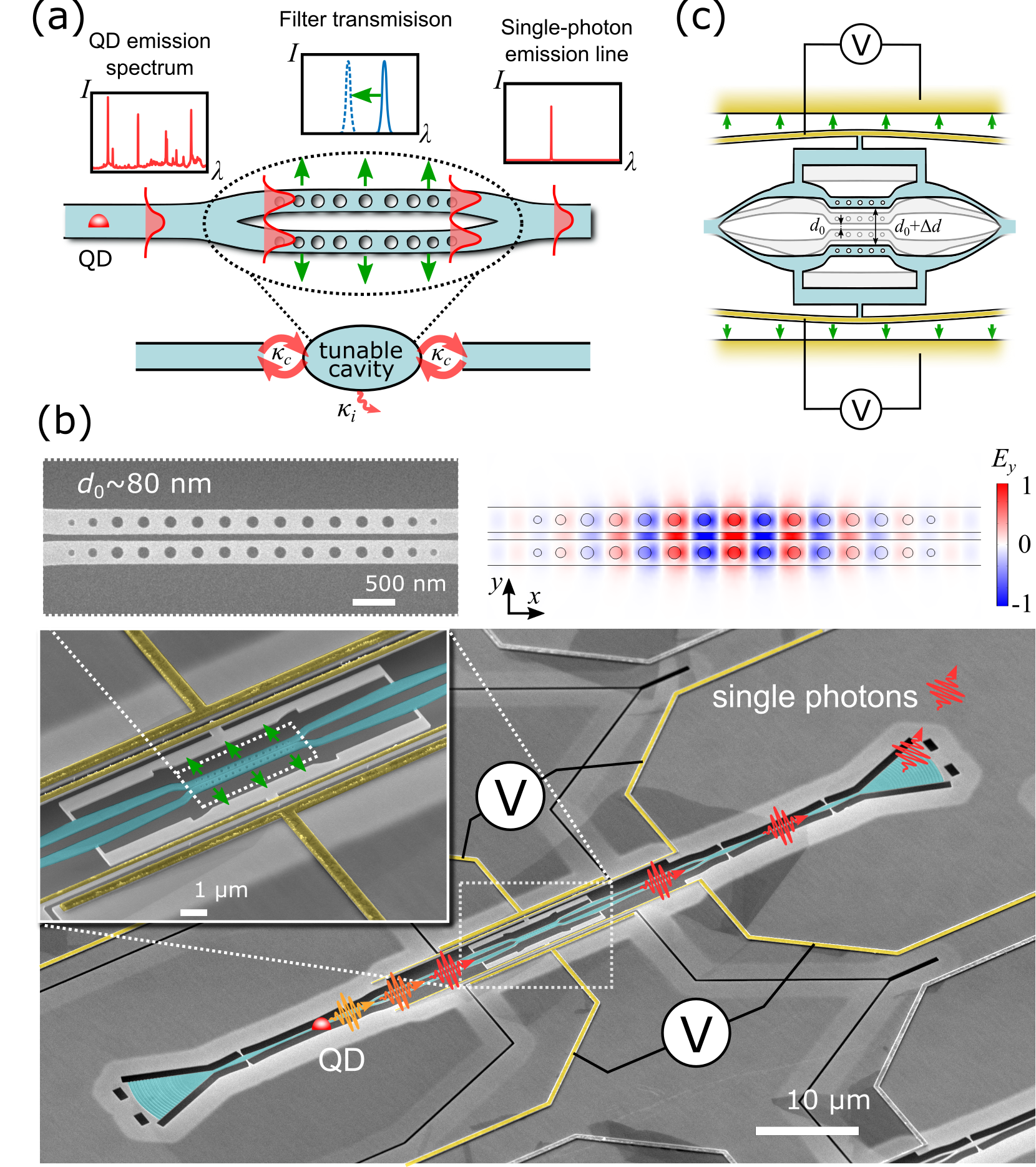
Device design and calibration. Figure 1(a) shows schematically the working principle of our reconfigurable filter, which is based on a coupled nanobeam photonic crystal cavity. Changing the distance between the nanobeams alters the coupling strength between them, resulting in a shift in the resonant wavelength of the cavity23. These structures have been widely studied in the context of optomechanics in various material platforms24, 25, 26, 27, 28, 29. Deotare et al. have used the coupled nanobeam photonic crystal cavity as a filter on silicon-on-insulator (SOI) and demonstrated spectral tuning with radiation pressure 30. Chew et al. reported micro-electromechanical devices on SOI to tune the resonance of a single nanobeam photonic crystal cavity31, 32. Yet, none of these works have shown waveguide-integration with a quantum emitter and on-chip filtering of a quantum dot single-photon source, which is what we demonstrate here.
The coupled cavity supports two sets of optical modes whose optical field profiles are either symmetric or anti-symmetric with respect to the nanobeam orientation23. We designed a circuit that couples, by means of adiabatic Y-splitters, a single-mode waveguide to the symmetric cavity modes (cf. the mode profile shown in the top panel of Fig. 1(b)). By suppressing the coupling to anti-symmetric modes, the filter provides a maximum transmission efficiency only limited by the scattering loss in the cavity.
The fabricated device is shown in the scanning electron micrograph (SEM) in Fig. 1(b), where InAs QDs and the tunable filter are monolithically integrated on a 160-nm thick GaAs membrane (See Supporting Information S1). The gap distance () between the two coupled nanobeams is controlled by a pair of electrostatic actuators12. By changing the voltage on the actuators, the filter can be tuned in resonance with a QD, allowing single photons to transit and reach a high-efficiency grating coupler33 on the other side. Details of the filter are shown in the inset of Fig. 1(b). A Y-shaped supporting frame is used to connect the metal electrodes to the waveguides, avoiding direct contact with the cavity region and enabling parallel motion of the nanobeams, as shown in Fig. 1(c). The top panel of Fig. 1(b) shows the detail of the cavity, which is designed using the envelope equation approach outlined in Supporting Information S2.1: the lattice constant is stretched following a nearly-quadratic law to pull a single optical mode from the air-band of the photonic crystal into the bandgap34. Mode matching between the photonic crystal Bloch modes and the waveguide modes is optimized by tapering the radii of two external holes 35.
Our designed filter has a FSR of 25 nm and an intrinsic quality factor . For a cavity coupled to a waveguide, the transmission coefficient is given by36
| (1) |
where and are cavity-waveguide coupling rate and cavity intrinsic loss rate, respectively, and are the quality factors corresponding to and , and is the quality factor of the waveguide-loaded cavity calculated as . We design the cavity to support a fundamental mode with , which provides theoretically near-unity transmission efficiency (). By chosing an initial nanobeam separation nm, a total wavelength shift of nm is expected, based on finite-element method simulations (see Supporting Information S2 for details on the device design and simulations).
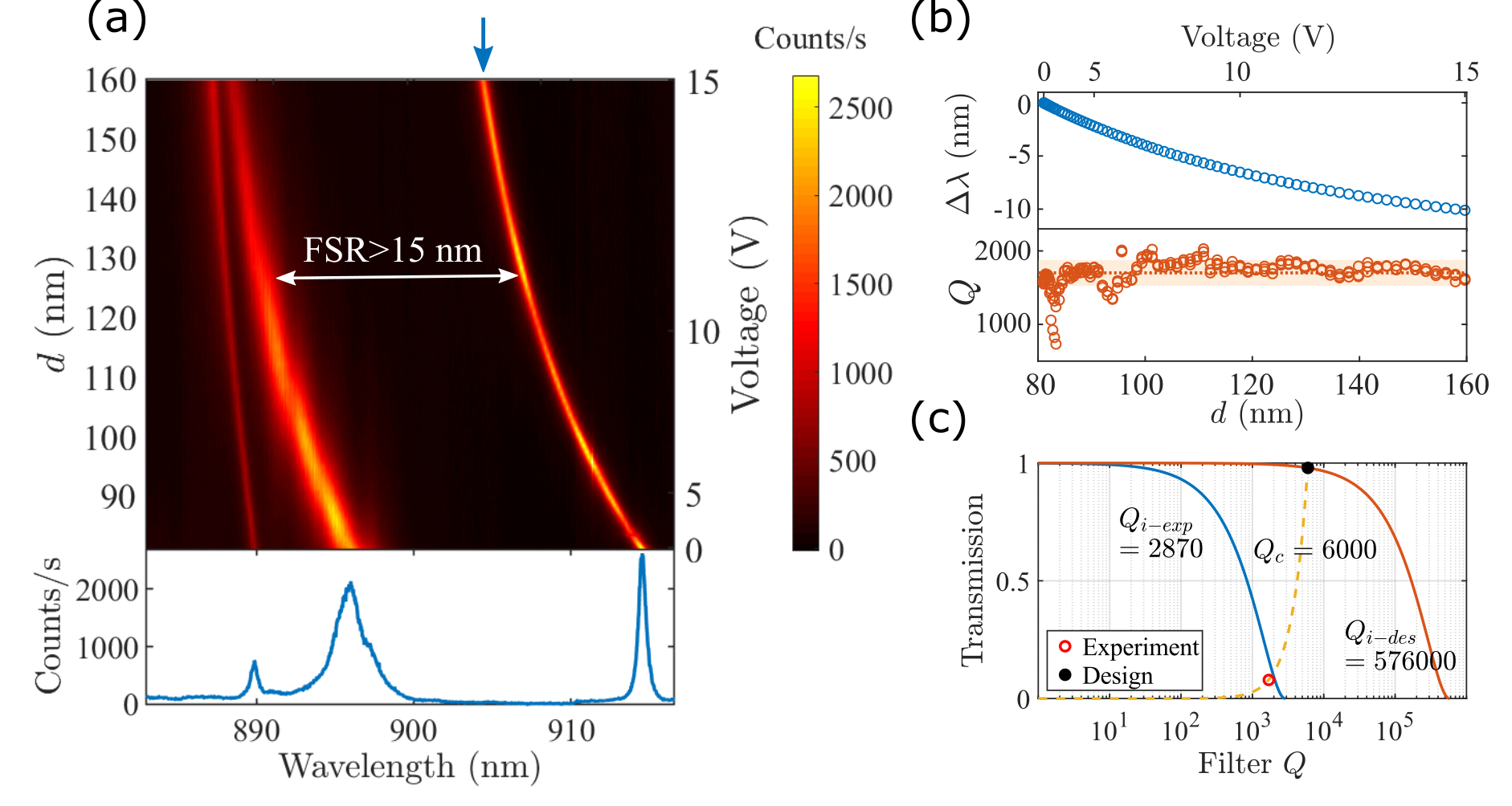
The NOEMS filter is characterized in a helium-flow cryostat at the temperature of 10 K. The excitation laser beam (at 800 nm wavelength) is focused on one grating coupler with high pumping power far above the saturation level of individual excitonic transitions. The photoluminescence from the QD ensemble is used as a broadband light source to probe the filter response. Light transmitted through the filter is collected from a second grating coupler and sent to a spectrometer. Figure 2(a) shows the collected spectra as a function of the applied voltage and mechanical displacement (see Supporting Information S2 for details on the calibration of the voltage-displacement curve). Two transmission peaks at 914.5 nm and 896 nm (cf. bottom panel of Fig. 2(a)), corresponding to the fundamental and second-order modes of the cavity, respectively, are blue-shifted by over 10 nm with 15 V applied bias. Another transmission peak around 890 nm, which is not predicted by theory, is also visible, but with a much smaller tuning range. We attribute this mode to fabrication disorder that causes localization of light into one of the two nanobeams37 and thus is only weakly affected by the mechanical displacement. The absence of any red-shifting modes indicates that the device is indeed symmetric (See Supporting Information S2.1). The FSR of the filter extends over 15 nm and covers a large part of the QD distribution. The transmission peaks of the fundamental mode are fitted with a Lorentzian function, and the resulting wavelength shift and quality factor are plotted in Fig. 2(b). The cavity resonance blue-shifts when increasing , with a maximum optomechanical coupling rate 97 GHz/nm (or nm/nm) at nm. The filter linewidth is 0.54 nm, corresponding to a cavity , which is not significantly affected by the mechanical tuning. A maximum tuning range of nm is observed by increasing the bias up to 15 V, which is close to the electrostatic pull-in failure of the device. An even larger tuning range ( nm) is observed on another device, albeit with a slightly lower (See Supporting Information S3.3).
By normalizing the transmission signal to that of an identical structure without photonic crystal cavity, we extract an averaged peak transmission efficiency of . Both experimental transmission and are lower than the theoretical values, as shown in Fig. 2(c). We attribute this mismatch to fabrication imperfections, e.g., resist residues, rough waveguide sidewalls, and non-uniformity of photonic-crystal holes, which cause a large drop in the intrinsic quality factor. This is verified by measuring the quality factor of cavities decoupled from the waveguides, providing an experimental (See Supporting Information S3.2). Figure 2(c) shows the expected transmission (cf. Eq. 1) as a function of the total filter in the case where the intrinsic quality factor is the theoretical (red line) or the experimental (blue line). The observed transmission (red dot) fits very well to the theoretical curve, indicating that transmission can be further improved by optimizing the fabrication process to reduce out-of-plane losses.
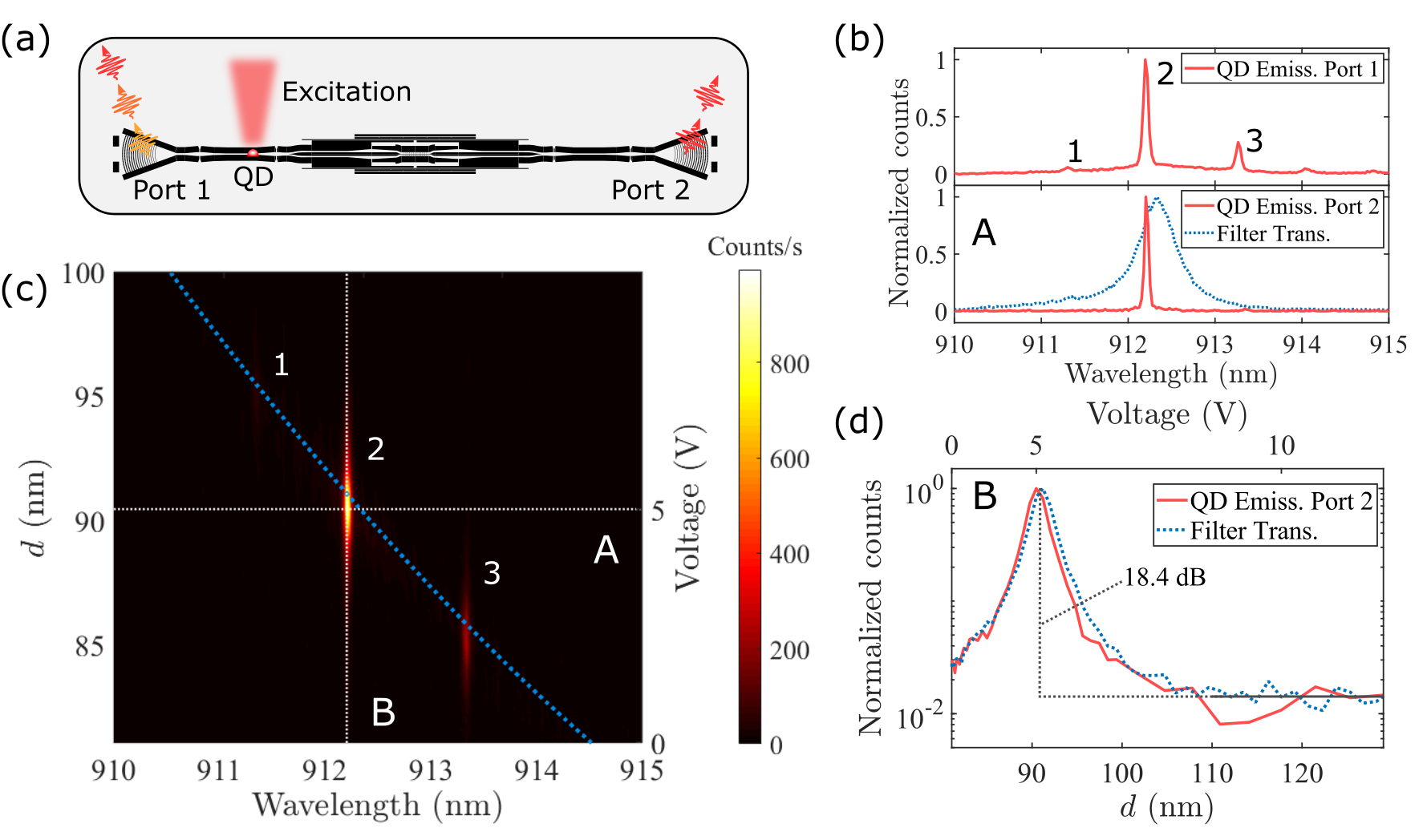
Single-photon filtering. Figure 3 demonstrates single-photon filtering with the electromechanically reconfigurable on-chip filter. The excitation and collection scheme is shown in Fig. 3(a), where we use the grating named Port 1 as reference for unfiltered QD emission, and Port 2 for the filtered signal. The measured QD emission spectra from both ports are shown in Fig. 3(b) when the cavity is tuned in resonance with the emitter. Three QD emission lines are seen in the unfiltered spectrum in the top panel. By applying a voltage bias at 5 V, we align the cavity resonance to a bright QD emission line (line 2 in the figure) at 912.2 nm, and filter out the other two lines (1 and 3), which are no longer visible in the Port 2 spectrum (cf. upper and lower panel of Fig. 3(b)). The tunable filter provides around 10 dB rejection to nearby emission lines on both sides. The advantage of a reconfigurable filter is that, in fact, one can perform selective filtering of any QD emission lines within the tuning range, as shown in the map of Fig. 3(c). At voltage biases of 3.2 V and 6 V, the filter resonance can be aligned to two more QD lines (1 and 3, at 913.3 nm and 911.3 nm, respectively). Unlike the traditional thermo-optic tuning methods, the mechanical approach does not introduce any cross-talk with the QDs, which is confirmed by the absence of shift in the emitter energy.
The extinction ratio (ER) is obtained from both the collected QD emission counts around 912.2 nm (cut-line B in Fig. 3(c)) and the cavity transmission at the same wavelength, as shown in Fig. 3(d). Comparing the peak transmission with averaged counts at gap distance nm ( nm), we obtain consistent ER values of 18.5 dB and 18.3 dB from the QD and filter transmission data, respectively. The experimental ER is likely limited by fabrication disorder in the photonic crystal structure.
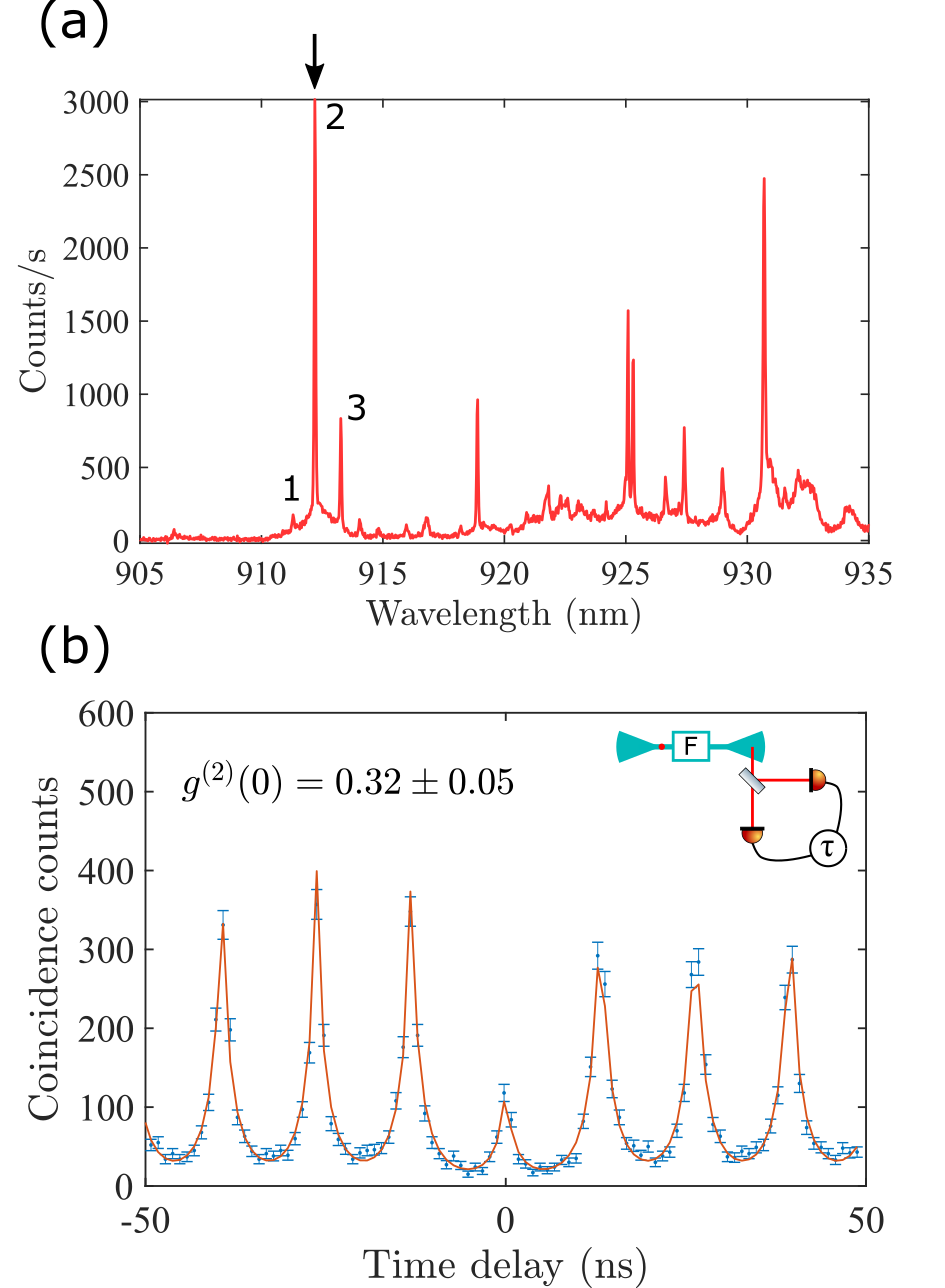
To verify on-chip single-photon filtering, we measure the purity of the filtered single photons with a pulsed Hanbury Brown-Twiss (HBT) experiment. Figure 4(a) shows the unfiltered emission spectrum collected from Port 1 (the same data as Fig. 3(b) upper panel but with a broader spectral range). Multiple excitonic transmissions are visible over a 25 nm wavelength range due to the above-band excitation. We consider line 2 at 912.2 nm (cf. Fig. 4a) and adjust the pump to , where nW is the saturation power of the transition. The measured autocorrelation of the filtered QD emission line 2 is plotted in Fig. 4(b), where a clear signature of single-photon emission is observed at zero time delay, with . We note that the QD emission collected from Port 2 after the on-chip filter is sent directly to the HBT set-up without additional filtering, as schematically shown in the inset. The is still limited by the above-band excitation scheme, the high QD density (10 m-2), and the finite ER of the on-chip filter. Yet, our recorded is only slightly larger than the typical obtained with off-chip filtering using above-band excitation38, 20, 21, 12, 39, indicating comparable single-photon filtering performance.
Discussion. Transmission (or insertion loss) of the on-chip filter is a very important figure-of-merit for quantum experiments, and the current transmission of our device can be improved through different methods. Equation 1 shows that there is a trade-off between transmission and (or filter bandwidth) for a given , as shown in Fig. 2(c) for both and . The transmission of the fabricated device (the red circle) is lower than the design (the black dot), but it fits very well to the theoretical transmission calculated by fixing to the design value (yellow dashed line), indicating nearly no loss from the cavity-waveguide interface. Higher transmission can be achieved by lowering (e.g., reducing the number of holes forming the cavity), at the cost of a lower total . Alternatively, the intrinsic quality factor can be increased by optimizing the fabrication process, which results in simutaneoulsy improved transmission and narrower filter linewidth. Using a hard mask for reactive ion etching of GaAs40 or performing surface passivation41, 42 could greatly improve the intrinsic cavity . As a quantitative prospect, nanobeam photonic crystal cavities with have been demonstrated in suspended GaAs membrane platform43, suggesting that % is within reach with the proposed design. Increasing the would also enable applications such as filtering of phonon sidebands, that requires around 40 GHz bandwidth () to produce high-indistinguishability photons10.
Conclusion & Outlook. We have demonstrated single-photon filtering with a nanomechanically reconfigurable nanophotonic cavity, which is monolithically integrated with a QD single-photon source. The device is operated at 10 K without any cross-talk with the emitter. Thanks to the enhanced opto-electro-mechanical interaction at the nanoscale, a large tunablity of nm at a bias of 15 V can be achieved, comparable to the inhomogeneous spectral distribution of QD emission. The filter design, together with the small footprint of m2, is intrinsically low-loss and scalable. A high ER of dB and a large FSR nm ensure good single-photon purity.
The device reported here has the salient features of a broadband device which could be replicated for multiple emitters on the same chip. Combined with a -- diode structure for the Stark tuning of the excitonic transitions8, on-chip sources can be realized and scaled by controlling both the emitter and the filter resonances44. Furthermore, positioning the QDs inside the cavity and tuning the cavity in-resonance with the QD emission, promises to improve both single-photon generation efficiency and indistinguishability with Purcell effect45, 18. A single on-chip filter can also replace multiple off-chip filtering setups, which are required in multi-path experiments, e.g. on-chip demultiplexing12, 46, where the single-photon source is routed to many different outputs. The tunable filter reported in this work constitutes an important building block for scaling these experiments further, towards a fully-integrated photonic quantum information processing with multiple qubits.
We gratefully acknowledge financial support from Innovationsfonden (Quantum Innovation Center QUBIZ), Danmarks Grundforskningsfond (DNRF) (Center for Hybrid Quantum Networks (Hy-Q)), H2020 European Research Council (ERC) (SCALE) & ERC-Proof of Concept (FIPS 790206), Bundesministerium für Bildung und Forschung (BMBF) (16KIS0867, Q.Link.X), Deutsche Forschungsgemeinschaft (DFG) (TRR 160), Styrelsen for Forskning og Innovation (FI) (5072-00016B QUANTECH).
The authors thank Henri Thyrrestrup for helpful discussion.
References
- O’Brien et al. 2009 O’Brien, J. L.; Furusawa, A.; Vučković, J. Photonic quantum technologies. Nat. Photonics 2009, 3, 687
- Carolan et al. 2015 Carolan, J. et al. Universal linear optics. Science 2015, 349, 711–716
- Flamini et al. 2018 Flamini, F.; Spagnolo, N.; Sciarrino, F. Photonic quantum information processing: a review. Rep. Prog. Phys. 2018, 82, 016001
- Arcari et al. 2014 Arcari, M.; Söllner, I.; Javadi, A.; Lindskov Hansen, S.; Mahmoodian, S.; Liu, J.; Thyrrestrup, H.; Lee, E. H.; Song, J. D.; Stobbe, S.; Lodahl, P. Near-unity coupling efficiency of a quantum emitter to a photonic crystal Waveguide. Phys. Rev. Lett. 2014, 113, 093603
- Luxmoore et al. 2013 Luxmoore, I. J.; Wasley, N. A.; Ramsay, A. J.; Thijssen, A. C. T.; Oulton, R.; Hugues, M.; Kasture, S.; Achanta, V. G.; Fox, A. M.; Skolnick, M. S. Interfacing Spins in an InGaAs Quantum Dot to a Semiconductor Waveguide Circuit Using Emitted Photons. Phys. Rev. Lett. 2013, 110, 037402
- Ding et al. 2019 Ding, D.; Appel, M. H.; Javadi, A.; Zhou, X.; Löbl, M. C.; Söllner, I.; Schott, R.; Papon, C.; Pregnolato, T.; Midolo, L., et al. Coherent optical control of a quantum-dot spin-qubit in a waveguide-based spin-photon interface. Phys. Rev. Appl. 2019, 11, 031002
- Wang et al. 2019 Wang, H. et al. Towards optimal single-photon sources from polarized microcavities. Nat. Photonics 2019, 1–6
- Kiršanskė et al. 2017 Kiršanskė, G. et al. Indistinguishable and efficient single photons from a quantum dot in a planar nanobeam waveguide. Phys. Rev. B 2017, 96, 165306
- Javadi et al. 2015 Javadi, A.; Söllner, I.; Arcari, M.; Hansen, S. L.; Midolo, L.; Mahmoodian, S.; Kiršanskė, G.; Pregnolato, T.; Lee, E.; Song, J.; Stobbe, S.; Lodahl, P. Single-photon non-linear optics with a quantum dot in a waveguide. Nat. Commun. 2015, 6, 8655
- Lodahl et al. 2015 Lodahl, P.; Mahmoodian, S.; Stobbe, S. Interfacing single photons and single quantum dots with photonic nanostructures. Rev. Mod. Phys. 2015, 87, 347
- Hepp et al. 2019 Hepp, S.; Jetter, M.; Portalupi, S. L.; Michler, P. Semiconductor quantum dots for integrated quantum photonics. Adv. Quantum Technol. 2019, 2, 1900020
- Papon et al. 2019 Papon, C.; Zhou, X.; Thyrrestrup, H.; Liu, Z.; Stobbe, S.; Schott, R.; Wieck, A. D.; Ludwig, A.; Lodahl, P.; Midolo, L. Nanomechanical single-photon routing. Optica 2019, 6, 524–530
- Sprengers et al. 2011 Sprengers, J.; Gaggero, A.; Sahin, D.; Jahanmirinejad, S.; Frucci, G.; Mattioli, F.; Leoni, R.; Beetz, J.; Lermer, M.; Kamp, M.; Höfling, S.; Sanjines, R.; Fiore, A. Waveguide superconducting single-photon detectors for integrated quantum photonic circuits. Appl. Phys. Lett. 2011, 99, 181110
- Reithmaier et al. 2015 Reithmaier, G.; Kaniber, M.; Flassig, F.; Lichtmannecker, S.; Müller, K.; Andrejew, A.; Vuckovic, J.; Gross, R.; Finley, J. On-chip generation, routing, and detection of resonance fluorescence. Nano Lett. 2015, 15, 5208–5213
- Schwartz et al. 2018 Schwartz, M.; Schmidt, E.; Rengstl, U.; Hornung, F.; Hepp, S.; Portalupi, S. L.; llin, K.; Jetter, M.; Siegel, M.; Michler, P. Fully on-chip single-photon Hanbury-Brown and Twiss experiment on a monolithic semiconductor–superconductor platform. Nano Lett. 2018, 18, 6892–6897
- Lodahl 2017 Lodahl, P. Quantum-dot based photonic quantum networks. Quantum Sci. Technol. 2017, 3, 013001
- Santori et al. 2001 Santori, C.; Pelton, M.; Solomon, G.; Dale, Y.; Yamamoto, Y. Triggered single photons from a quantum dot. Phys. Rev. Lett. 2001, 86, 1502–1505
- Iles-Smith et al. 2017 Iles-Smith, J.; McCutcheon, D. P.; Nazir, A.; Mørk, J. Phonon scattering inhibits simultaneous near-unity efficiency and indistinguishability in semiconductor single-photon sources. Nat. Photonics 2017, 11, 521
- Dusanowski et al. 2019 Dusanowski, L.; Kwon, S.-H.; Schneider, C.; Höfling, S. Near-unity indistinguishability single photon source for large-scale integrated quantum optics. Phys. Rev. Lett. 2019, 122, 173602
- Elshaari et al. 2017 Elshaari, A. W.; Zadeh, I. E.; Fognini, A.; Reimer, M. E.; Dalacu, D.; Poole, P. J.; Zwiller, V.; Jöns, K. D. On-chip single photon filtering and multiplexing in hybrid quantum photonic circuits. Nat. Commun. 2017, 8, 379
- Elshaari et al. 2018 Elshaari, A. W.; Büyüközer, E.; Zadeh, I. E.; Lettner, T.; Zhao, P.; Schöll, E.; Gyger, S.; Reimer, M. E.; Dalacu, D.; Poole, P. J.; Jöns, K. D.; Zwiller, V. Strain-tunable quantum integrated photonics. Nano Lett. 2018, 18, 7969–7976
- Midolo et al. 2018 Midolo, L.; Schliesser, A.; Fiore, A. Nano-opto-electro-mechanical systems. Nat. Nanotechnol. 2018, 13, 11
- Haus et al. 1987 Haus, H.; Huang, W.; Kawakami, S.; Whitaker, N. Coupled-mode theory of optical waveguides. J. Light. Technol. 1987, 5, 16–23
- Deotare et al. 2009 Deotare, P. B.; McCutcheon, M. W.; Frank, I. W.; Khan, M.; Lončar, M. Coupled photonic crystal nanobeam cavities. Appl. Phys. Lett. 2009, 95, 031102
- Perahia et al. 2010 Perahia, R.; Cohen, J.; Meenehan, S.; Alegre, T. M.; Painter, O. Electrostatically tunable optomechanical “zipper” cavity laser. Appl. Phys. Lett. 2010, 97, 191112
- Frank et al. 2010 Frank, I. W.; Deotare, P. B.; McCutcheon, M. W.; Lončar, M. Programmable photonic crystal nanobeam cavities. Opt. Express 2010, 18, 8705–8712
- Midolo et al. 2012 Midolo, L.; Yoon, S.; Pagliano, F.; Xia, T.; Van Otten, F.; Lermer, M.; Höfling, S.; Fiore, A. Electromechanical tuning of vertically-coupled photonic crystal nanobeams. Opt. Express 2012, 20, 19255–19263
- Tian et al. 2019 Tian, F.; Sumikura, H.; Kuramochi, E.; Takiguchi, M.; Ono, M.; Shinya, A.; Notomi, M. All-optical dynamic modulation of spontaneous emission rate in hybrid optomechanical cavity quantum electrodynamics systems. arXiv preprint arXiv:1901.07691 2019,
- Mouradian and Englund 2017 Mouradian, S. L.; Englund, D. A tunable waveguide-coupled cavity design for scalable interfaces to solid-state quantum emitters. APL Photonics 2017, 2, 046103
- Deotare et al. 2012 Deotare, P. B.; Bulu, I.; Frank, I. W.; Quan, Q.; Zhang, Y.; Ilic, R.; Loncar, M. All optical reconfiguration of optomechanical filters. Nat. Commun. 2012, 3, 846
- Chew et al. 2010 Chew, X.; Zhou, G.; Yu, H.; Chau, F. S.; Deng, J.; Loke, Y. C.; Tang, X. An in-plane nano-mechanics approach to achieve reversible resonance control of photonic crystal nanocavities. Opt. Express 2010, 18, 22232–22244
- Chew et al. 2011 Chew, X.; Zhou, G.; Chau, F. S.; Deng, J. Nanomechanically tunable photonic crystal resonators utilizing triple-beam coupled nanocavities. IEEE Photon. Technol. Lett. 2011, 23, 1310–1312
- Zhou et al. 2018 Zhou, X.; Kulkova, I.; Lund-Hansen, T.; Hansen, S. L.; Lodahl, P.; Midolo, L. High-efficiency shallow-etched grating on GaAs membranes for quantum photonic applications. Appl. Phys. Lett. 2018, 113, 251103
- Quan and Loncar 2011 Quan, Q.; Loncar, M. Deterministic design of wavelength scale, ultra-high Q photonic crystal nanobeam cavities. Opt. Express 2011, 19, 18529–18542
- Sauvan et al. 2005 Sauvan, C.; Lecamp, G.; Lalanne, P.; Hugonin, J.-P. Modal-reflectivity enhancement by geometry tuning in photonic crystal microcavities. Opt. Express 2005, 13, 245–255
- Joannopoulos et al. 2008 Joannopoulos, J. D.; Johnson, S. G.; Winn, J. N.; Meade, R. D. Photonic Crystals: Molding the Flow of Light, 2nd Ed. Princeton University Press 2008,
- García et al. 2017 García, P. D.; Kiršanskė, G.; Javadi, A.; Stobbe, S.; Lodahl, P. Two mechanisms of disorder-induced localization in photonic-crystal waveguides. Phys. Rev. B 2017, 96, 144201
- Daveau et al. 2017 Daveau, R. S.; Balram, K. C.; Pregnolato, T.; Liu, J.; Lee, E. H.; Song, J. D.; Verma, V.; Mirin, R.; Nam, S. W.; Midolo, L., et al. Efficient fiber-coupled single-photon source based on quantum dots in a photonic-crystal waveguide. Optica 2017, 4, 178–184
- Schnauber et al. 2019 Schnauber, P.; Schall, J.; Bounouar, S.; Höhne, T.; Park, S.-I.; Ryu, G.-H.; Heindel, T.; Burger, S.; Song, J.-D.; Rodt, S., et al. Deterministic integration of quantum dots into on-chip multi-mode interference couplers via in-situ electron beam lithography. European Quantum Electronics Conference. 2019; p eb_2_2
- González et al. 2014 González, I. P.; Muñoz Camuñez, L. E.; Taboada, A. G.; Robles Urdiales, C.; Ripalda Cobián, J. M.; Postigo Resa, P. A. Fabrication of high quality factor GaAs/InAsSb photonic crystal microcavities by inductively coupled plasma etching and fast wet etching. J. Vac. Sci. Technol. B 2014, 32, 011204
- Guha et al. 2017 Guha, B.; Marsault, F.; Cadiz, F.; Morgenroth, L.; Ulin, V.; Berkovitz, V.; Lemaître, A.; Gomez, C.; Amo, A.; Combrié, S.; Gérard, B.; Leo, G.; Favero, I. Surface-enhanced gallium arsenide photonic resonator with quality factor of 6. Optica 2017, 4, 218–221
- Liu et al. 2018 Liu, J.; Konthasinghe, K.; Davanço, M.; Lawall, J.; Anant, V.; Verma, V.; Mirin, R.; Nam, S. W.; Song, J. D.; Ma, B.; Chen, Z. S.; Ni, H. Q.; Niu, Z. C.; Srinivasan, K. Single Self-Assembled Quantum Dots in Photonic Nanostructures: The Role of Nanofabrication. Phys. Rev. Appl. 2018, 9, 064019
- Enderlin et al. 2012 Enderlin, A.; Ota, Y.; Ohta, R.; Kumagai, N.; Ishida, S.; Iwamoto, S.; Arakawa, Y. High guided mode–cavity mode coupling for an efficient extraction of spontaneous emission of a single quantum dot embedded in a photonic crystal nanobeam cavity. Phys. Rev. B 2012, 86, 075314
- Petruzzella et al. 2018 Petruzzella, M.; Birindelli, S.; Pagliano, F.; Pellegrino, D.; Zobenica, Ž.; Li, L.; Linfield, E.; Fiore, A. Quantum photonic integrated circuits based on tunable dots and tunable cavities. APL Photonics 2018, 3, 106103
- Midolo et al. 2012 Midolo, L.; Pagliano, F.; Hoang, T.; Xia, T.; van Otten, F.; Li, L.; Linfield, E.; Lermer, M.; Höfling, S.; Fiore, A. Spontaneous emission control of single quantum dots by electromechanical tuning of a photonic crystal cavity. Appl. Phys. Lett. 2012, 101, 091106
- Lenzini et al. 2017 Lenzini, F.; Haylock, B.; Loredo, J. C.; Abrahão, R. A.; Zakaria, N. A.; Kasture, S.; Sagnes, I.; Lemaitre, A.; Phan, H.-P.; Dao, D. V., et al. Active demultiplexing of single photons from a solid-state source. Laser Photonics Rev. 2017, 11, 1600297