Low-Damping Ferromagnetic Resonance in Electron-Beam Patterned, High- Vanadium Tetracyanoethylene Magnon Cavities
Abstract
Integrating patterned, low-loss magnetic materials into microwave devices and circuits presents many challenges due to the specific conditions that are required to grow ferrite materials, driving the need for flip-chip and other indirect fabrication techniques. The low-loss ( ), room-temperature ferrimagnetic coordination compound vanadium tetracyanoethylene () is a promising new material for these applications that is potentially compatible with semiconductor processing. Here we present the deposition, patterning, and characterization of thin films with lateral dimensions ranging from 1 micron to several millimeters. We employ electron-beam lithography and liftoff using an aluminum encapsulated poly(methyl methacrylate), poly(methyl methacrylate-methacrylic acid) copolymer bilayer (PMMA/P(MMA-MAA)) on sapphire and silicon. This process can be trivially extended to other common semiconductor substrates. Films patterned via this method maintain low-loss characteristics down to 25 microns with only a factor of 2 increase down to 5 microns. A rich structure of thickness and radially confined spin-wave modes reveals the quality of the patterned films. Further fitting, simulation, and analytic analysis provides an exchange stiffness, , as well as insights into the mode character and surface spin pinning. Below a micron, the deposition is non-conformal, which leads to interesting and potentially useful changes in morphology. This work establishes the versatility of for applications requiring highly coherent magnetic excitations ranging from microwave communication to quantum information.
Interest in low-loss magnetic thin films has been growing due to potential applications in magnonics and quantum information as well as the potential for compact, high-efficiency magnetoelectric devices.Cheng et al. (2018); Nikitin et al. (2015); Chumak, Serga, and Hillebrands (2017) In the field of magnonics and spintronics, yttrium iron garnet (, YIG), an electrically insulating ferrite that exhibits extremely low Gilbert damping, and a linewidth of 3.4 G at 9.6 GHz for pristine nanometer-thick films, is currently the leading material for magnetoelectronic circuits.Chang et al. (2014); Hauser et al. (2016) The low-damping present in YIG films has led to its incorporation in magnetoelectric circuits and it also plays a prominent role in the study of magnonics research.Serga, Chumak, and Hillebrands (2010); Schneider et al. (2008); Zahwe et al. (2010); Nikitin et al. (2015); Chumak (2019) Patterning of YIG, however, presents a challenge. When patterned, the damping increases to to for ion-milled films,Hahn et al. (2014); Jungfleisch et al. (2015) and to for liftoff-based films.Krysztofik et al. (2017); Li et al. (2016); Zhu et al. (2017) Furthermore, post-growth annealing steps at temperatures as high as 850 are generally required to attain even these degraded damping values, and the lowest damping values are only achieved for films deposited on the lattice-matching substrate gadolinium gallium garnet (, GGG), both of which provide strict limits on direct integration with functional devices.Onbasli et al. (2014); Manuilov and Grishin (2010); Manuilov et al. (2009) Vanadium tetracyanoethylene (, ), on the other hand, is a low-loss (sub-Gauss linewidth at 9.83 GHz), room-temperature ( 600 K) ferrimagnet that can be deposited optimally at and without the need for lattice matching.Harberts et al. (2015); Yu et al. (2014) These relatively benign deposition conditions allow for deposition on a wide variety of substrates and pre-patterned circuits, positioning as an exciting option for on-chip magnetic and magnonic device incorporation.Zhu et al. (2016); Liu et al. (2018); Chilcote et al. (2019) However, realizing this promise has been limited by the lack of techniques for patterning films at micron to sub-micron length scales.
Here we present a method for depositing and patterning using standard electron-beam lithography techniques with additional steps to preserve its high and low-loss characteristics. The primary hurdles to micron-scale pattering of are its sensitivity to oxygen and solvents traditionally used in fabrication. Our past work has addressed air-sensitivity via encapsulation in a commercial organic light-emitting diode (OLED) epoxy, increasing its lifetime in air from hours to months,Froning et al. (2015) and there are other commercial options, such as potting,Bardoliwalla that promise to protect films indefinitely. This leaves solvent sensitivity, which inhibits the use of traditional patterning techniques for two reasons: i) the presence of solvent in the resist layer inhibits the deposition of as the solvent outgasses during growth, and ii) liftoff requires a solvent soak that will in general destroy or degrade the CVD-grown film. Here we address both of these challenges by using a thin encapsulating layer for the resist and identifying a -compatible solvent, respectively, demonstrating micron-scale patterning of films with no apparent increase in microwave loss. The patterned structures are characterized by scanning electron microscopy (SEM) and by a combination of ferromagnetic resonance (FMR) and comparison with micromagnetic simulations and analytic calculations.
The CVD thin-film growth process typically results in a smooth blue-black film uniformly distributed across the substrate surface. When a resist is applied to the substrate before growth, however, deposition results in non-uniform coverage and poor quality. This is attributed to chemical reactions between the released solvents and the precursors (tetracyanoethylene and vanadium hexacarbonyl). Solvents present in common resists including LOR, MICROPOSIT S1800 series, and poly(methyl methacrylate) result in macroscopically inconsistent deposition of across the resist’s surface as well as inside patterned areas. In order to address this solvent sensitivity, a layer of aluminum is thermally deposited after development to encapsulate the resist layer. The aluminum is then oxidized with a ten-minute ultraviolet ozone clean in a UVOCS T10x10/OES prior to deposition.
In prior precipitation synthesis studies,Thorum, Pokhodnya, and Miller (2006); Pokhodnya et al. (2001); Zhang et al. (1996) several solvents have been shown to precipitate with a modest impact on the of the resulting powder. Since dichloromethane has a small impact on quality and readily dissolves poly(methyl methacrylate) (PMMA) and poly(methyl methacrylate-methacrylic acid 8.5%) (P(MMA 8.5 MAA)) at room temperature, this is the resist-solvent pair chosen to address the challenge of solvent based liftoff. Specifically, this work focuses on 495PMMA A6 on MMA (8.5) MAA EL 11 as a resist bilayer (PMMA/P(MMA 8.5 MAA)) to additively pattern low-loss onto sapphire, with the understanding that this patterning process should trivially extend to other inorganic substrates.Tseng et al. (2003); Tennant and Bleier (2016)
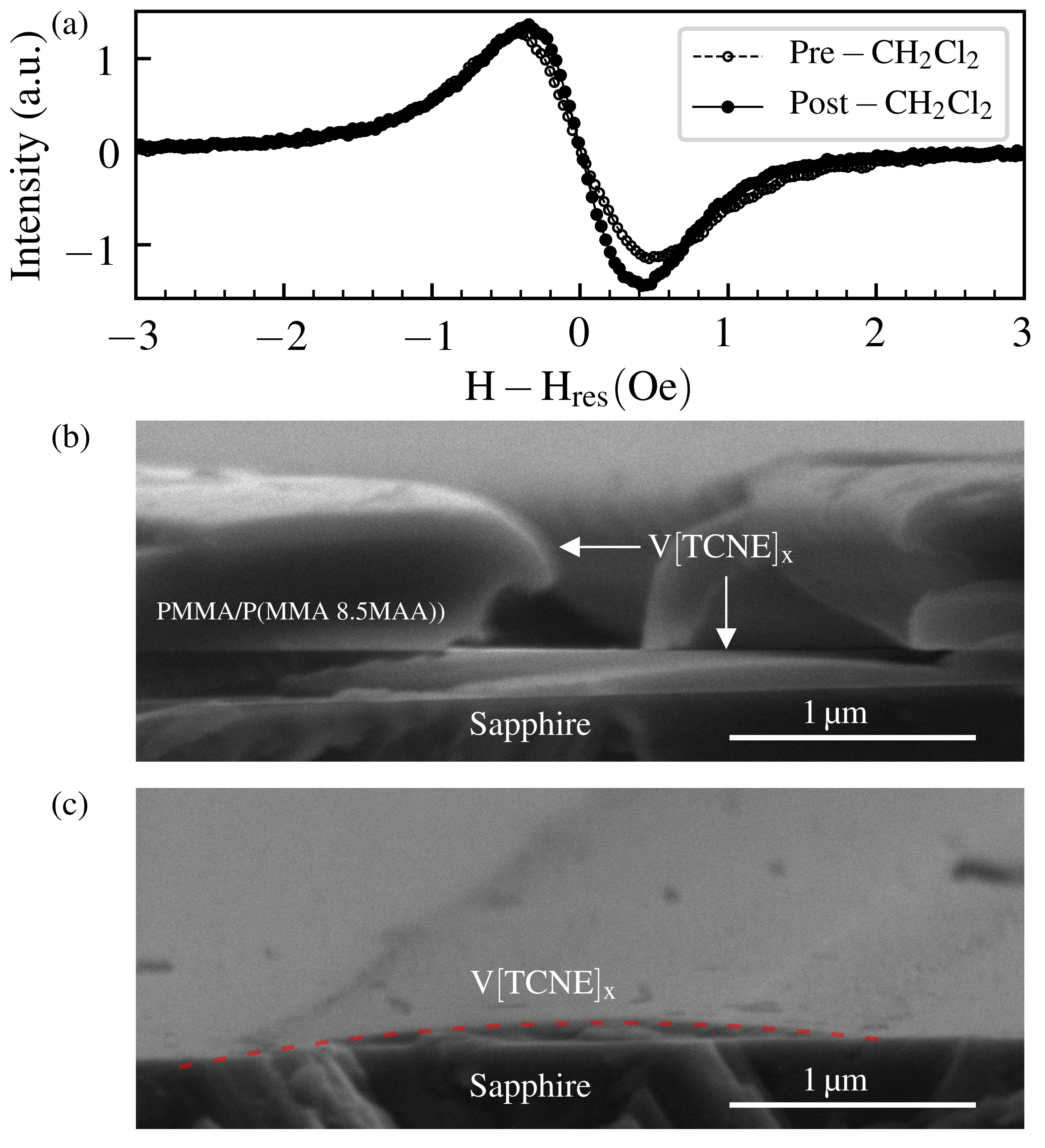
Figure 1(a) shows the FMR response at 9.83 GHz of a thin film before and after a 2.5-hour soak in dichloromethane in a nitrogen atmosphere (< 10 ppm , < 2 ppm ). The linewidth and lineshape of the resonance are largely unchanged, indicating that there is little to no incorporation of dichloromethane into the CVD-grown film on that timescale. The linewidth narrows slightly, possibly due to changes in the ordering of the due to solvent annealing.Hu et al. (2014) The growth morphology that results from the above process is characterized by SEM and is shown in Fig. 1(b-c). Unlike physical vapor deposition, CVD deposition is driven by a combination of flow and diffusion. Figure 1(b) shows how the deposition is limited by the flow characteristics through the patterned features. In particular, does not form vertical sidewalls but rather forms gently sloped sidewalls at an angle of about over a distance of approximately a micron from the edge. This leads to a parabolic profile, as one would expect from the velocity profile resulting from laminar flow through a channel, Fig. 1(c). These results suggest that there are likely opportunities to tune the structure profile by controlling channel width, flow direction, resist height, and resist morphology. This cross-sectional profile is difficult to achieve with other material systems and deposition techniques,Tait, Smy, and Brett (1993) and it may prove beneficial for studies of spin-wave confinement as it offers a means to realize an approximation of an adiabatic boundary.
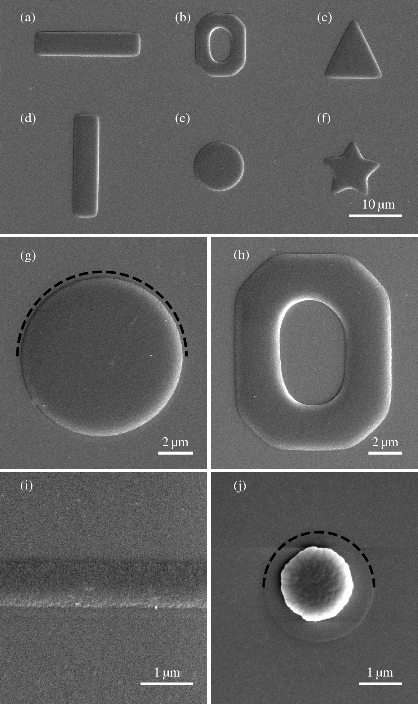
Flow-limited deposition can, in principle, also lead to anisotropy in patterned features based on alignment between the flow direction and internal structure. Figure 2 shows various patterned structures of that are designed to explore these effects. The images show that there is anisotropic growth for several of the structures. The deposition time for these samples is 1.0 hr, leading to a nominal thickness of 300 nm. All shapes in Fig. 2 have a faint outline that reveals the ballistically deposited layer. In Figs. 2(g, j), a dashed black semi-circle has been superimposed over the outline to make it easier to compare the and morphology. The outline shows that there is little to no offset or ellipticity present in the patterned diameter disk. Figure 2(h), however, shows significant anisotropy as measured by the differences between the faint outline and the pattern. The flow direction across the shape is left to right with a tilt towards the top. The flow direction manifests in a more complete, laminar profile along the top and bottom whereas eddies inhibit deposition in the left and right interior edges. Laminar flow over a step predicts an eddy approximately as wide as the step is tall.Shankar and Deshpande (2000); Taneda (1979) This is consistent with the fact that the 540 nm thick PMMA/P(MMA 8.5 MAA)) bilayer results in a roughly wide region of reduced flow which leads to a taper in the morphology. This effect is also seen in Figs. 2(c, f) where the concave features at the corners see a reduction in deposition roughly away from the planned shape shown by each peak.
Figures 2(i, j) further explore the impacts of length scale on gas flow and growth morphology using bars and disks. The wide bar in Fig. 2(i) acts as a channel for gas flow, yielding a parabolic deposition profile similar to Fig. 1(b, c) across the shape and good filling of the ballistic profile when the thickness of the bar in Fig. 2(i) is about 200 nm thick. In contrast, the diameter disk in Fig. 2(j) is visibly off-center, with a 100 nm offset towards the top-left of the . The deposition morphology in Fig. 2(j) resembles the eddy flow structure from boundary-driven flow into a cavity with a depth-to-width ratio of one-third, suggesting that flow over the features is laminar and the resulting deposition shape and cross-section can be simulated from flow.Shankar and Deshpande (2000); Taneda (1979) It may be possible to achieve smaller features by using thinner resist layers, or by choosing pattern geometries that intentionally channel the flow, but these approaches will be pattern specific and are beyond the scope of this work.
To explore the utility of this patterning technique for magnonic and magnetoelectric devices, the magnetization dynamics of these microstructures are studied using FMR. Measurements are performed at room temperature in a Bruker EPR spectrometer with the microwave frequency held near 9.83 GHz while the applied magnetic field is swept across the resonance. Scans are then repeated for multiple polar angles, , from out-of-plane ( , OOP) to in-plane ( , IP) and for multiple azimuthal angles, , from parallel to the -axis ( ) to perpendicular to the -axis ( ).
Figure 3 shows the results of FMR characterization of wide bars aligned parallel to the -axis and diameter disks. The bars are spaced center to center in a 1D array and the disks are spaced center to center in a 2D, square array. The position of the uniform mode of the bars (red) and disks (blue) is tracked as a function of orientation in Figs. 3(b, c). The bars show a single-peaked resonance that varies from 3550 to 3630 Oe as the structures are rotated IP to OOP. The disks reveal a more complicated peak structure, that suggests standing spin-wave modes are present, Fig. 3(i), and exhibit a larger field difference between IP and OOP resonances. This difference is evident in Fig. 3(d) where the resonances are tracked through multiple high-symmetry directions, revealing the full anisotropy of these structures.
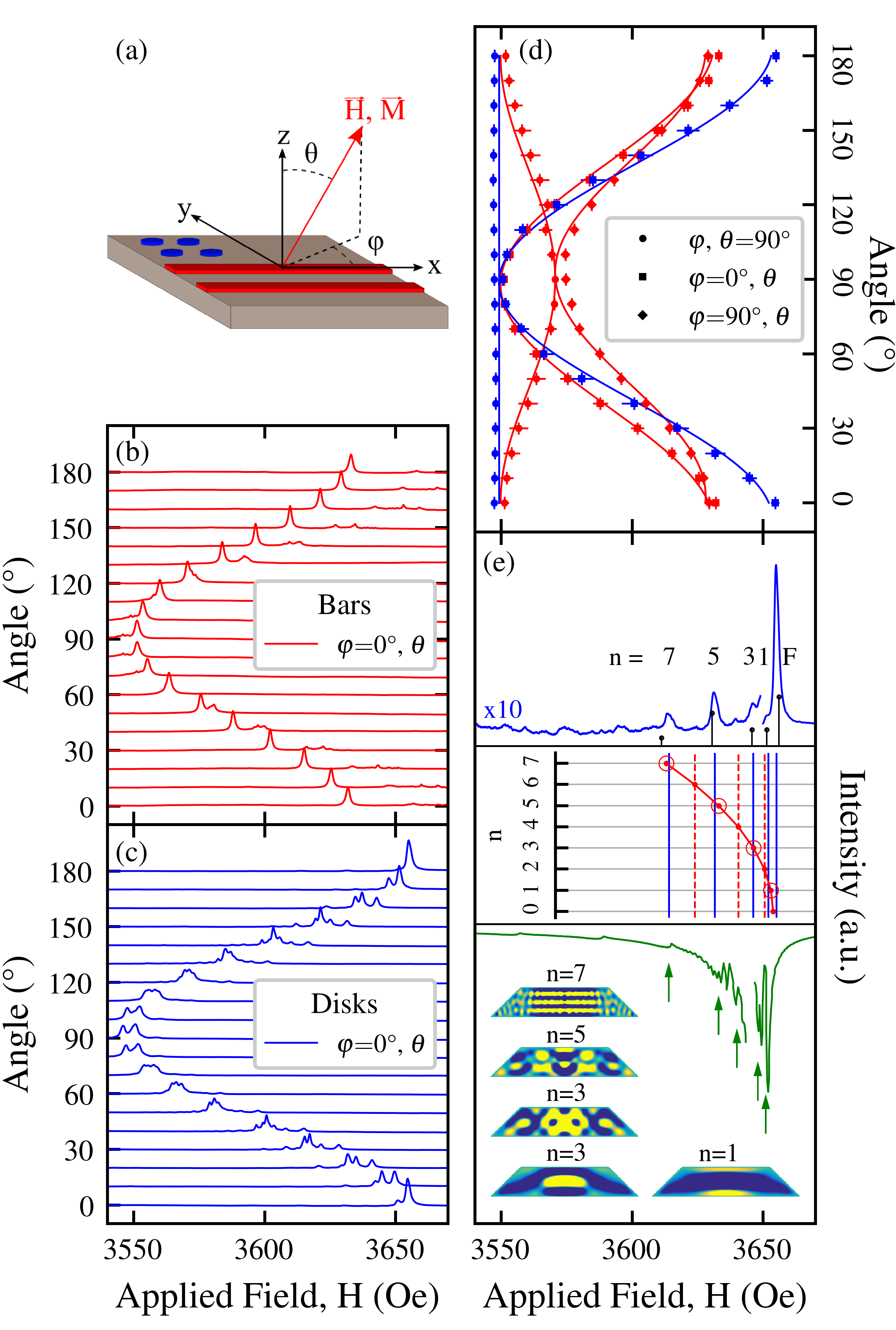
The formalism developed by Smit, Beljers, and SuhlSuhl (1955); Smit and Beljers (1955); Baselgia et al. (1988) is used to model this anisotropy. A Cartesian coordinate system is defined with parallel to the length, parallel to the width, and parallel to the thickness of the bars as shown in Fig. 3(a). By explicitly considering the Zeeman and magnetostatic contributions to the free energy, , one derives the expression,Smit and Wijn (1954); Morrish (2001)
| (1) |
where are the components of the applied magnetic field, are the components of the magnetization, and are components of the demagnetizing tensor, which leads to shape anisotropy, with defined with respect to pattern axes. Solving for harmonic solutions with respect to time and minimizing with respect to and yields
| (2) |
where
| (3a) | |||
| (3b) |
are the diagonal components of the demagnetizing tensor, is the polar angle, and is the azimuthal angle that the sample magnetization makes with the pattern axes, Fig. 3(a). Equation 2 is derived assuming the demagnetizing field is parallel to the magnetization, so , and that the magnetization, , is parallel to the applied field, , so only one set of angles is needed to describe the magnetization and applied field, . This approximation is validated by the fact that for is less than 95 G, and the applied magnetic fields used for these measurements are 3500 to 3750 Oe. As a result, is parallel to to within 1.5 degrees for the experiments shown here.
The other potential source of anisotropy is the crystal field which arises from the local coordination of the exchange interaction. For uniaxial crystal-field anisotropy, this crystal field can be decomposed into components acting along the pattern axes with the same angular dependence as the demagnetizing anisotropy. As a result, the that are extracted from the fit to Eq. 2 are a combination of demagnetizing-field and crystal-field components with the form
| (4) |
where is the observed anisotropy tensor component, is the geometric demagnetizing tensor component, and is the additional crystal field along that axis.
Three anisotropy tensors are used to determine the strength of the crystal field in the bars and the disks. The first, , is generated from simultaneous fits to the three red anisotropy curves in Fig. 3(d) from the bar array to Eq. 2. These fits yield G and MHz/Oe, which agree with literature values,Zhu et al. (2016); Yu et al. (2014) and , , and . The trace of this anisotropy tensor is , indicating the magnitude of the crystal-field contribution is Oe. Using SEM measurements to geometrically determine a pure demagnetizing tensor for the bars, , that does not include crystal-field effects yields , , and .Smith et al. (2010) Comparing the with these , the direction shows the largest difference of 0.09, indicating this crystal field is oriented along the -axis of the bars. The magnitude of this crystal field is consistent with previous measurements of templated nanowires.Chilcote et al. (2019) In addition to being self-consistent, these results also predict the anisotropy curves for the disks (blue lines in Fig. 3(d)). To test these fitting results, a final demagnetizing tensor, , for the disk are calculated as and based on SEM measurements and demagnetizing expressions from the literature.Kraus (1973) Combining this with the and values from the previous fit results in the solid blue curves shown in Fig. 3(d) with a combined reduced chi-squared value of 0.96. Adding crystal-field effects degrades the quality of the reduced chi-squared value for Oe, indicating the absence of crystal-field effects in the disks. These results suggest the crystal-field contribution arises from anisotropic relaxation in the patterned bars, which corroborates prior work with nanowires where an additional in-plane crystal field is reported due to anisotropy in the relaxation of the templated structures.Chilcote et al. (2019)
The more complicated spectra of the disks suggests that the disks are acting as spin-wave cavities with complex internal mode structure, Fig. 3(e). Numerical simulations and analytical calculations are carried out to better understand this mode structure. To begin characterizing the mode structure, the strongest experimental peaks are compared with the odd analytic thickness modes predicted for a thin film in the OOP geometry.Kalinikos and Slavin (1986) The vertical blue lines in Fig. 3(e) represent the experimental peak values. Fitting to these peak values using the mode assignments indicated in Fig. 3(e) and the parameters obtained from the FMR measurements yields the red analytic curve and a value of the exchange stiffness, . The even thickness modes, shown as dashed red lines, agree well with smaller peaks within the experimental data. Analytic disk calculations shown in black in Fig. 3(e) further describe the identity of the quantum confined modes and agree well when using this . The exchange stiffness depends on ; an approximate form, found by several means,Skomski et al. (2003); Skomski (2004); Moreno et al. (2016) is . The exchange length constant is therefore a better metric to use to compare samples with different saturation magnetizations. The difference between the exchange length from this study of nm and the previously reported value of 21 nmZhu et al. (2016) could be due to differences in grain structure between the patterned and unpatterned filmsMoreno et al. (2016) as well as difficulty in mode assignment, , in prior work where fewer modes are visible.
Numeric modeling is performed using time-domain micromagnetic simulations with the open-source GPU-based software MuMax3 while using the material parameters determined from the fits to the experimental data.Vansteenkiste et al. (2014) The factors that have the most relevant influence on the simulated peak structure are (i) the sloped sidewalls that (a) have a strong effect on the shape of the lowest frequency set of peaks which are comprised of a set of closely-spaced radially and lowest-order thickness quantized modes and (b) apply an overall shift to the thickness confined modes, (ii) the pinning conditions of the surfaces that have a strong effect on the amplitudes of the thickness-confined modes, and (iii) the exchange stiffness, , that controls the spacing between thickness quantized modes. Sloped sidewalls are used in the simulations to replicate the shape that occurs due to the slower growth rate within 1 micron of the resist. The simulations show that the position of the most prominent peak relative to the thickness-confined modes is sensitive to the exact shape of the sidewalls and the pinning conditions. To account for small differences in the slope of simulated and experimental data, the higher-order thickness modes are aligned with experiment instead of the uniform mode in Fig. 3(e). Simulations with perfect pinning at the top and bottom surfaces agree better with the experimentally observed thickness and radial confined mode structure as compared to simulations with top, bottom, or no pinning; however, the close agreement between the calculated even-mode resonance fields and several smaller peaks in the experimental spectrum suggests that one of the surfaces likely has slightly weaker pinning than the other. Additional simulations can be found in the supplement. The resulting simulated frequency response of the simulation is in green in Fig. 3(e) along with several mode maps at peaks indicated by the green arrows. These maps reveal quantization in the thickness and radial directions in the tapered structure. The lower-order thickness modes each show distinct radial quantization. The thickness mode, shows a nearly pure thickness quantization and represents the sum of multiple closely-spaced radials modes that are excited simultaneously. The agreement between simulated and experimental spectra demonstrates control over the spin-wave mode structure and lays the foundation for the study and application of magnon cavities with adiabatic boundaries and engineered mode structures.
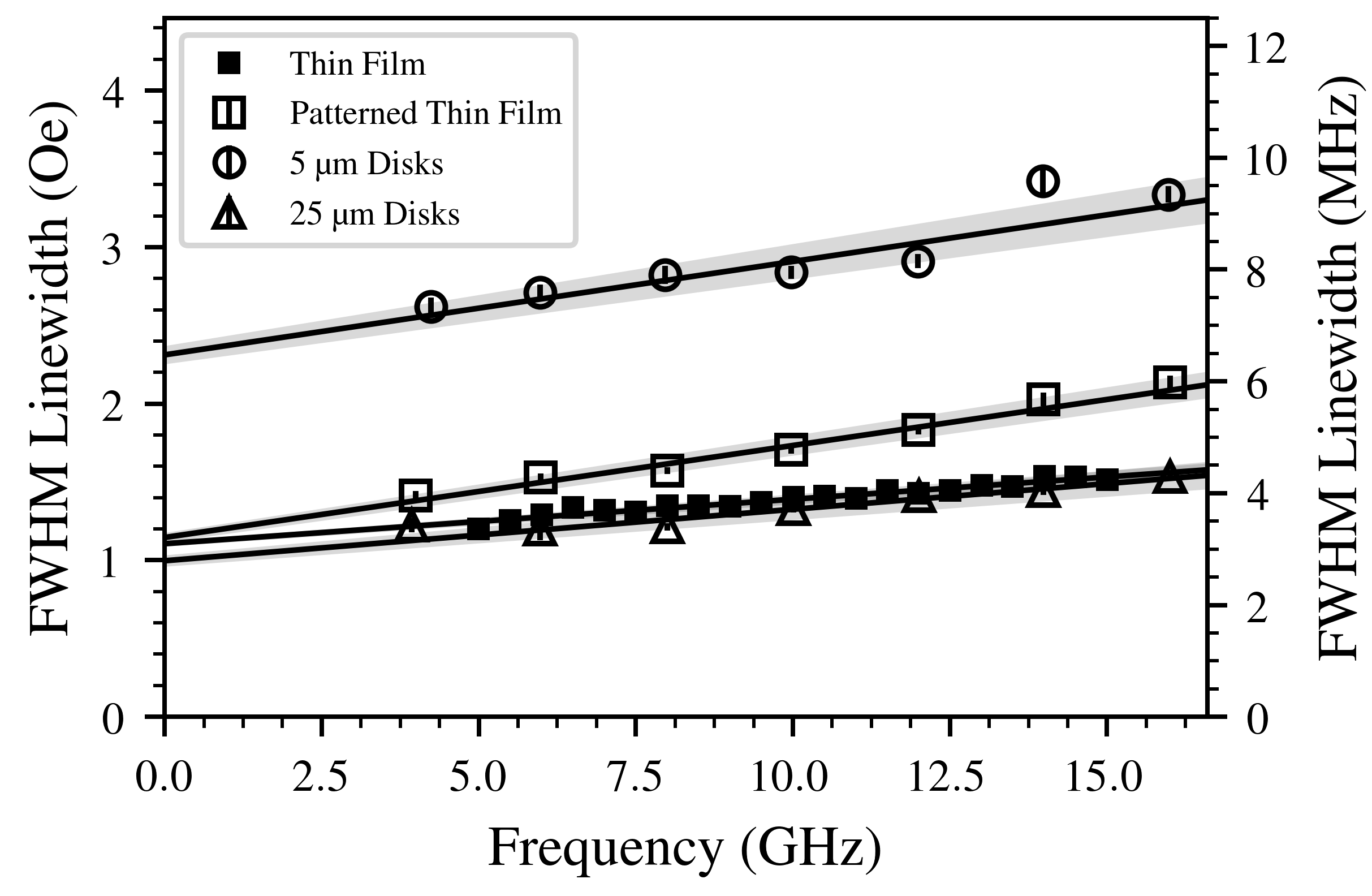
In addition to analyzing anisotropy and mode structure, FMR can be used to determine the total magnetic loss, or damping of these magnon modes. This damping potentially contains both homogeneous and inhomogeneous sources as parameterized via the Gilbert damping factor, .Kalarickal et al. (2006) The damping for the patterned films is measured via broadband ferromagnetic resonance (BFMR) performed in a custom built microstrip-based system wherein the applied magnetic field is held constant in the OOP geometry and the microwave frequency is swept across the resonance. Figure 4 shows the linewidth vs frequency extracted for representative samples of disks and unpatterned films, with vertical lines indicated the error in the fits. Representative raw data and fits can be found in the supplemental information. The Gilbert damping is fit using Suhl’s expression for the full-width at half-maximum (FWHM) FMR linewidth,Suhl (1955)
| (5) |
in combination with phenomenological inhomogeneous broadening.Heinrich, Cochran, and Hasegawa (1985) This results in
| (6) |
when one uses for the OOP geometry.Kalarickal et al. (2006) In Eq. 6, is the FWHM linewidth of the resonance, is the Gilbert damping, and is the FWHM contribution from inhomogeneous broadening. The fits yield = for unpatterned films, = for features, and = for disks. The thin-film damping result of places films comfortably alongside YIG films as the lowest magnetic damping material currently available, and the retention of that ultra-low damping after patterning is considerably better than the reported values for patterned YIG structures.Hahn et al. (2014); Jungfleisch et al. (2015); Krysztofik et al. (2017); Li et al. (2016); Zhu et al. (2017) In addition to low-damping, the high-frequency measurements of the thin film and disks have Quality () factors, , of over 3,700, competitive with factors for YIG thin films.Balinskiy et al. (2017) Retaining ultra-low damping and high in patterned for features as small as and as large as millimeters, both relevant length scales for many magnonic cavity applications,Chumak, Serga, and Hillebrands (2014, 2017); Cornelissen et al. (2018); Morris et al. (2017); Zhang et al. (2014); Zhu et al. (2017) combined with the flexibility to deposit on most inorganic substrates, positions to complement YIG in magnonic and magnetoelectric devices where integration of GGG or high-temperature annealing steps is limiting, such as for small form factors and on-chip integration.
In summary, this work demonstrates a method for patterning the ferrimagnetic coordination compound vanadium tetracyanoethylene. Standard electron-beam lithography of PMMA/P(MMA-MAA) bilayers is used in conjunction with pre-growth aluminum encapsulation and post-growth dichloromethane liftoff to pattern thin films with no degradation of the microwave magnetic properties. The sidewalls of structures patterned in this way are sloped, allowing for the investigation and quantitative modeling of spin-wave confinement in magnetic structures with soft boundary conditions. Patterned films with features down to exhibit a high of over 3,700 and ultra-low damping of which are competitive with unpatterned YIG and lower than all existing reports of patterned YIG microstructures.Hahn et al. (2014); Jungfleisch et al. (2015); Krysztofik et al. (2017); Li et al. (2016); Zhu et al. (2017) The versatility of the patterning and deposition conditions of , in combination with its ultra-low magnetic damping, position as a promising candidate for incorporation into magnetoelectric devices where low-loss, highly coherent, magnon excitation are desirable. Such applications range from microwave communications to quantum information.
Supplementary Materials
See supplementary material for the a detailed description of sample fabrication, measurement techniques, simulations, and analytic calculations.
Acknowledgements.
This work is supported by Emerging Frontiers in Research and Innovation (EFRI) Grant No. EFMA-1741666. The authors acknowledge the NanoSystems Laboratory at The Ohio State University.References
- Cheng et al. (2018) Y. Cheng, B. Peng, Z. Hu, Z. Zhou, and M. Liu, “Recent development and status of magnetoelectric materials and devices,” Physics Letters A 382, 3018–3025 (2018).
- Nikitin et al. (2015) A. Nikitin, A. Ustinov, A. Semenov, A. Chumak, A. Serga, V. I. Vasyuchka, E. Lahderanta, B. Kalinikos, and B. Hillebrands, “Width-modulated magnonic crystal and its application for spin-wave logic,” 2015 European Microwave Conference (EuMC) (2015), 10.1109/eumc.2015.7345998.
- Chumak, Serga, and Hillebrands (2017) A. V. Chumak, A. A. Serga, and B. Hillebrands, “Magnonic crystals for data processing,” Journal of Physics D: Applied Physics 50, 244001 (2017).
- Chang et al. (2014) H. Chang, P. Li, W. Zhang, T. Liu, A. Hoffmann, L. Deng, and M. Wu, “Nanometer-thick yttrium iron garnet films with extremely low damping,” IEEE Magnetics Letters 5, 1–4 (2014).
- Hauser et al. (2016) C. Hauser, T. Richter, N. Homonnay, C. Eisenschmidt, M. Qaid, H. Deniz, D. Hesse, M. Sawicki, S. G. Ebbinghaus, and G. Schmidt, “Yttrium iron garnet thin films with very low damping obtained by recrystallization of amorphous material,” Scientific Reports 6 (2016), 10.1038/srep20827.
- Serga, Chumak, and Hillebrands (2010) A. A. Serga, A. V. Chumak, and B. Hillebrands, “YIG magnonics,” Journal of Physics D: Applied Physics 43, 264002 (2010).
- Schneider et al. (2008) T. Schneider, A. A. Serga, B. Leven, B. Hillebrands, R. L. Stamps, and M. P. Kostylev, “Realization of spin-wave logic gates,” Applied Physics Letters 92, 022505 (2008).
- Zahwe et al. (2010) O. Zahwe, B. Abdel Samad, B. Sauviac, J. P. Chatelon, M. F. Blanc Mignon, J. J. Rousseau, M. Le Berre, and D. Givord, “Yig thin film used to miniaturize a coplanar junction circulator,” Journal of Electromagnetic Waves and Applications 24, 25–32 (2010).
- Chumak (2019) A. V. Chumak, “Magnon spintronics,” Spintronics handbook: Spin transport and magnetism, second edition , 247–302 (2019).
- Hahn et al. (2014) C. Hahn, V. V. Naletov, G. de Loubens, O. Klein, O. d’ Allivy Kelly, A. Anane, R. Bernard, E. Jacquet, P. Bortolotti, V. Cros, and et al., “Measurement of the intrinsic damping constant in individual nanodisks of and |Pt,” Applied Physics Letters 104, 152410 (2014).
- Jungfleisch et al. (2015) M. B. Jungfleisch, W. Zhang, W. Jiang, H. Chang, J. Sklenar, S. M. Wu, J. E. Pearson, A. Bhattacharya, J. B. Ketterson, M. Wu, and et al., “Spin waves in micro-structured yttrium iron garnet nanometer-thick films,” Journal of Applied Physics 117, 17D128 (2015).
- Krysztofik et al. (2017) A. Krysztofik, L. E. Coy, P. Kuświk, K. Załęski, H. Głowiński, and J. Dubowik, “Ultra-low damping in lift-off structured yttrium iron garnet thin films,” Applied Physics Letters 111, 192404 (2017).
- Li et al. (2016) S. Li, W. Zhang, J. Ding, J. E. Pearson, V. Novosad, and A. Hoffmann, “Epitaxial patterning of nanometer-thick films with low magnetic damping,” Nanoscale 8, 388–394 (2016).
- Zhu et al. (2017) N. Zhu, H. Chang, A. Franson, T. Liu, X. Zhang, E. Johnston-Halperin, M. Wu, and H. X. Tang, “Patterned growth of crystalline nanostructures with engineered magnetic shape anisotropy,” Applied Physics Letters 110, 252401 (2017).
- Onbasli et al. (2014) M. C. Onbasli, A. Kehlberger, D. H. Kim, G. Jakob, M. Kläui, A. V. Chumak, B. Hillebrands, and C. A. Ross, “Pulsed laser deposition of epitaxial yttrium iron garnet films with low gilbert damping and bulk-like magnetization,” APL Materials 2, 106102 (2014).
- Manuilov and Grishin (2010) S. A. Manuilov and A. M. Grishin, “Pulsed laser deposited films: Nature of magnetic anisotropy II,” Journal of Applied Physics 108, 013902 (2010).
- Manuilov et al. (2009) S. A. Manuilov, R. Fors, S. I. Khartsev, and A. M. Grishin, “Submicron film magnetostatic wave band pass filters,” Journal of Applied Physics 105, 033917 (2009).
- Harberts et al. (2015) M. Harberts, Y. Lu, H. Yu, A. J. Epstein, and E. Johnston-Halperin, “Chemical vapor deposition of an organic magnet, vanadium tetracyanoethylene,” Journal of Visualized Experiments (2015), 10.3791/52891.
- Yu et al. (2014) H. Yu, M. Harberts, R. Adur, Y. Lu, P. C. Hammel, E. Johnston-Halperin, and A. J. Epstein, “Ultra-narrow ferromagnetic resonance in organic-based thin films grown via low temperature chemical vapor deposition,” Applied Physics Letters 105, 012407 (2014).
- Zhu et al. (2016) N. Zhu, X. Zhang, I. H. Froning, M. E. Flatté, E. Johnston-Halperin, and H. X. Tang, “Low loss spin wave resonances in organic-based ferrimagnet vanadium tetracyanoethylene thin films,” Applied Physics Letters 109, 082402 (2016).
- Liu et al. (2018) H. Liu, C. Zhang, H. Malissa, M. Groesbeck, M. Kavand, R. McLaughlin, S. Jamali, J. Hao, D. Sun, R. A. Davidson, and et al., “Organic-based magnon spintronics,” Nature Materials 17, 308–312 (2018).
- Chilcote et al. (2019) M. Chilcote, M. Harberts, B. Fuhrman, K. Lehmann, Y. Lu, A. Franson, H. Yu, N. Zhu, H. Tang, G. Schmidt, and E. Johnston-Halperin, “Spin-wave confinement and coupling in organic-based magnetic nanostructures,” (2019), arXiv:1901.03286v1 [cond-mat.mtrl-sci] .
- Froning et al. (2015) I. H. Froning, M. Harberts, Y. Lu, H. Yu, A. J. Epstein, and E. Johnston-Halperin, “Thin-film encapsulation of the air-sensitive organic-based ferrimagnet vanadium tetracyanoethylene,” Applied Physics Letters 106, 122403 (2015).
- (24) D. Bardoliwalla, “Fast curing, low exotherm epoxy potting and encapsulating systems,” Proceedings: Electrical insulation conference and electrical manufacturing and coil winding conference 10.1109/eeic.1997.651053.
- Thorum, Pokhodnya, and Miller (2006) M. S. Thorum, K. I. Pokhodnya, and J. S. Miller, “Solvent enhancement of the magnetic ordering temperature () of the room temperature S (S=solvent, TCNE=tetracyanoethylene; 2) magnet,” Polyhedron 25, 1927–1930 (2006).
- Pokhodnya et al. (2001) K. I. Pokhodnya, D. Pejakovic, A. J. Epstein, and J. S. Miller, “Effect of solvent on the magnetic properties of the high-temperature molecule-based magnet,” Physical Review B 63 (2001), 10.1103/physrevb.63.174408.
- Zhang et al. (1996) J. Zhang, J. S. Miller, C. Vazquez, P. Zhou, W. B. Brinckerhoff, and A. J. Epstein, “Improved synthesis of the y(solvent) room-temperature magnet: Doubling of the magnetization at room temperature,” Molecule-Based Magnetic Materials , 311–318 (1996).
- Tseng et al. (2003) A. Tseng, K. Chen, C. Chen, and K. Ma, “Electron beam lithography in nanoscale fabrication: Recent development,” IEEE Transactions on Electronics Packaging Manufacturing 26, 141–149 (2003).
- Tennant and Bleier (2016) D. Tennant and A. Bleier, “Electron beam lithography of nanostructures,” Reference Module in Materials Science and Materials Engineering (2016), 10.1016/b978-0-12-803581-8.09255-9.
- Hu et al. (2014) S. Hu, O. Dyck, H. Chen, Y.-c. Hsiao, B. Hu, G. Duscher, M. Dadmun, and B. Khomami, “The impact of selective solvents on the evolution of structure and function in solvent annealed organic photovoltaics,” RSC Adv. 4, 27931–27938 (2014).
- Tait, Smy, and Brett (1993) R. Tait, T. Smy, and M. Brett, “Modelling and characterization of columnar growth in evaporated films,” Thin Solid Films 226, 196–201 (1993).
- Shankar and Deshpande (2000) P. N. Shankar and M. D. Deshpande, “Fluid mechanics in the driven cavity,” Annual Review of Fluid Mechanics 32, 93–136 (2000).
- Taneda (1979) S. Taneda, “Visualization of separating stokes flows,” Journal of the Physical Society of Japan 46, 1935–1942 (1979).
- Suhl (1955) H. Suhl, “Ferromagnetic resonance in nickel ferrite between one and two kilomegacycles,” Physical Review 97, 555–557 (1955).
- Smit and Beljers (1955) J. Smit and H. G. Beljers, “Ferromagnetic resonance absorption in , a highly anisotropic crystal,” Philips Res. Rep. 10, 113–130 (1955).
- Baselgia et al. (1988) L. Baselgia, M. Warden, F. Waldner, S. L. Hutton, J. E. Drumheller, Y. Q. He, P. E. Wigen, and M. Maryško, “Derivation of the resonance frequency from the free energy of ferromagnets,” Physical Review B 38, 2237–2242 (1988).
- Smit and Wijn (1954) J. Smit and H. Wijn, “Physical properties of ferrites,” Advances in Electronics and Electron Physics , 69–136 (1954).
- Morrish (2001) A. H. Morrish, “The physical principles of magnetism,” (2001), 10.1109/9780470546581.
- Smith et al. (2010) A. Smith, K. K. Nielsen, D. V. Christensen, C. R. H. Bahl, R. Bjørk, and J. Hattel, “The demagnetizing field of a nonuniform rectangular prism,” Journal of Applied Physics 107, 103910 (2010).
- Kraus (1973) L. Kraus, “The demagnetization tensor of a cylinder,” Czechoslovak Journal of Physics 23, 512–519 (1973).
- Kalinikos and Slavin (1986) B. A. Kalinikos and A. N. Slavin, “Theory of dipole-exchange spin wave spectrum for ferromagnetic films with mixed exchange boundary conditions,” Journal of Physics C: Solid State Physics 19, 7013–7033 (1986).
- Skomski et al. (2003) R. Skomski, A. Kashyap, Y. Qiang, and D. J. Sellmyer, “Exchange through nonmagnetic insulating matrix,” Journal of Applied Physics 93, 6477–6479 (2003).
- Skomski (2004) R. Skomski, “Nanomagnetic scaling,” Journal of Magnetism and Magnetic Materials 272-276, 1476–1481 (2004).
- Moreno et al. (2016) R. Moreno, R. F. L. Evans, S. Khmelevskyi, M. C. Muñoz, R. W. Chantrell, and O. Chubykalo-Fesenko, “Temperature-dependent exchange stiffness and domain wall width in Co,” Physical Review B 94 (2016), 10.1103/physrevb.94.104433.
- Vansteenkiste et al. (2014) A. Vansteenkiste, J. Leliaert, M. Dvornik, M. Helsen, F. Garcia-Sanchez, and B. Van Waeyenberge, “The design and verification of MuMax3,” AIP Advances 4, 107133 (2014).
- Kalarickal et al. (2006) S. S. Kalarickal, P. Krivosik, M. Wu, C. E. Patton, M. L. Schneider, P. Kabos, T. J. Silva, and J. P. Nibarger, “Ferromagnetic resonance linewidth in metallic thin films: Comparison of measurement methods,” Journal of Applied Physics 99, 093909 (2006).
- Heinrich, Cochran, and Hasegawa (1985) B. Heinrich, J. F. Cochran, and R. Hasegawa, “Fmr linebroadening in metals due to two-magnon scattering,” Journal of Applied Physics 57, 3690–3692 (1985).
- Balinskiy et al. (2017) M. Balinskiy, B. Mongolov, D. Gutierrez, H. Chiang, A. Slavin, and A. Khitun, “Perpendicularly magnetized YIG-film resonators and waveguides with high operating power,” AIP Advances 7, 056612 (2017).
- Chumak, Serga, and Hillebrands (2014) A. V. Chumak, A. A. Serga, and B. Hillebrands, “Magnon transistor for all-magnon data processing,” Nature Communications 5 (2014), 10.1038/ncomms5700.
- Cornelissen et al. (2018) L. Cornelissen, J. Liu, B. van Wees, and R. Duine, “Spin-current-controlled modulation of the magnon spin conductance in a three-terminal magnon transistor,” Physical Review Letters 120 (2018), 10.1103/physrevlett.120.097702.
- Morris et al. (2017) R. G. E. Morris, A. F. van Loo, S. Kosen, and A. D. Karenowska, “Strong coupling of magnons in a YIG sphere to photons in a planar superconducting resonator in the quantum limit,” Scientific Reports 7 (2017), 10.1038/s41598-017-11835-4.
- Zhang et al. (2014) X. Zhang, C.-L. Zou, L. Jiang, and H. X. Tang, “Strongly coupled magnons and cavity microwave photons,” Physical Review Letters 113 (2014), 10.1103/physrevlett.113.156401.
- LeCraw, Spencer, and Porter (1958) R. C. LeCraw, E. G. Spencer, and C. S. Porter, “Ferromagnetic resonance line width in yttrium iron garnet single crystals,” Physical Review 110, 1311–1313 (1958).