Selected graphenelike zigzag nanoribbons with chemically functionalized edges. Implications for electronic and magnetic properties
Abstract
It is known that there is a wide class of quasi 2-dimensional graphenelike nanomaterials which in many respects can outperform graphene. So, here in addition to graphene, the attention is directed to stanene (buckled honeycomb structure) and phosphorene (puckered honeycomb structure). It is shown that, depending on the doping, these materials can have magnetically ordered edges. Computed diagrams of magnetic phases illustrate that, on the one hand, n-type doped narrow zigzag nanoribbons of graphene and stanene have antiferromagnetically aligned magnetic moments between the edges. On the other hand, however, in case of phosphorene nanoribbons the zigzag edges can have ferromagnetically aligned magnetic moments for the p-type doping. The edge magnetism critically influences transport properties of the nanoribbons, and if adequately controlled can make them attractive for spintronics.
pacs:
72.25.-b, 75.75.-c, 72.80.Vp; 85.75.-dI Introduction
The great success of graphene has been followed by intensive studies of other two-dimensional nanostructures (2D NS’s). Here the main interest is in quasi 2D NS’s having either buckled or puckered structures. The well-known representative of the former structure is stanene (i.e. 2D Sn), whereas the latter is represented here by phosphorene. There is no doubt that graphene is quite attractive from the point of view of spintronic applications. In particular, its spin diffusion length is quite long, it reveals significant GMR Hill06 ; SK09 ; Yazyev10 and TMR Seneor12 effects, as well as pronounced non-local spin valve signals, and Hanle spin precessions Tombros07 . Noteworthy, narrow zigzag graphene nanoribbons have spontaneously magnetized edge atoms as predicted theoretically Fujita96 ; Soriano10 ; SK16 and next confirmed experimentally Magda14 ; Li14 . According to recent studies, the quasi 2D NS’s are not inferior to graphene as far as their attractiveness to spintronics is concerned. Band structure and edge magnetism issues in those materials have been recently intensively studied (see Refs.[Liu11, -SK18, ]). Remarkably, it has been demonstrated experimentally that oxidized phosphorene nanomashes have large magnetic moments at zigzag pore edges Nakanishi17 . Following this track, one of the main questions raised in this study is whether a similar effect occurs in the case of narrow zigzag-edge phosphorene nanoribbons.
II Modeling and computational details
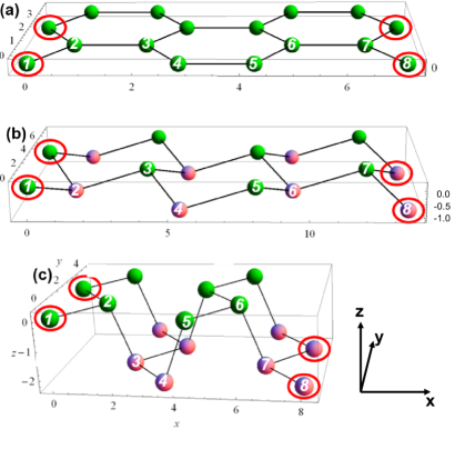
The buckled structure of stanene and the puckered structure of phosphorene are depicted in Figs.1 (b) and (c) (together with the reference graphene structure (a)). Two successive periodicity cells of the infinite zigzag ribbons in the y direction are shown.

| (1) |
| (2) |
| (3) |
| (4) |
| (5) |
where the first term describes interatomic hoppings, () describes mean-field Hubbard correlations in the out-of-plane (in-plane) magnetic configuration. takes into account possible edge functionalization with different chemical groups or by doping. In fact it is a usual on-site potential which is introduced in order to model these effects. For positive (negative) values of the occupation number of edge atoms gets reduced (enhanced) depending on whether dopant atoms are more (less) electronegative than the host atoms. Finally, the term describes intrinsic spin-orbit interaction Kane05 .
The other symbols used above have the following meanings: , , , , and is the Haldane factor equal to depending on wether the path between next nearest neighbor sites (i, j) is (or is not) clockwise.
Local magnetic moments for the out-of-plane and in-plane configurations are given by:
| (6) |
| (7) |
where the expectation values are taken over the ground state of (see [SK17, ] for details).
On the one hand the out-of-plane magnetic configurations () will be exemplified with graphene, eV, and phosphorene with as many as 5 hopping parameters (in eV) , , , , [Rudenko14, ,SK18, ]. On the other hand, in the buckled case, stanene with eV will be considered, its parameter eV [Ezawa15, ] is relatively large (Sn is much heavier than C and P) implying the appearance of magnetic anisotropy favoring the in-plane configuration Lado14 ; SK16 ; SK17 . Incidentally, results for the out-of-plane magnetic configuration and the in-plane one do not differ from each other if there is no anisotropy. In what follows, the energy unit is set to .
After solving the eigen-problem of the Hamiltonian (1), spin-dependent energy bands, numbers of forward propagating modes (ballistic transmission and hence spin-dependent conductance () can be found SK17 :
| (8) |
III Discussion of the results
III.1 Magnetic phase diagrams
It is important to be aware that edge magnetism is strongly energy-dependent (sensitive to the electron filling). Typically it appears at energies close to the chemical potential , and disappears outside this region. The ground state magnetic configuration can be determined by comparing grand canonical potentials corresponding to different possible magnetic alignments (cf. [SK17, ]).
Figure 2 illustrates the phase diagram of possible arrangements of mutual orientations of edge magnetic moments in graphene (panel (a)), stanene (b) and phosphorene (c). Noteworthy close to the chemical potential the magnetic phases can appear. In the case of graphene and stanene the antiferromagnetic alignment between the edges is possible for the doping parameter =0 and -0.1, whereas phosphorene can be ferromagnetically aligned for =0 and 0.1 and 0.2. It means that the edge magnetism is favored if graphene and stanene are not less electronegative than the dopants, in contrast to phosphorene where it is advantageous if its electronegativity does not exceed that of the dopants.

III.2 Electrical conductance and edge magnetism of graphene and stanene
As shown for graphene in [Magda14, ] (experiment and theory), as well as in [Chen17, ] (theory), a typical situation is that narrow zigzag nanoribbons initially have the AF configuration, which gives way to the F configuration for increasing width.
As to stanene nanoribbons, the situation resembles that of graphene, as shown in [Fu17, ] the AF configuration constitutes the ground state (with edge atom magnetic moments slightly smaller than in graphene). In [Qi18, ] it is also reported that AF configuration has the lowest energy, but the energy difference decreases with the increasing width (up to the calculated width of W=16 zigzag lines).
Figures 3 and 4 show spin dependent conductances in the vicinity of in graphene and stanene NR’s (10 zigzag lines wide). Up- and down-spin conductances are represented by up and down-oriented triangles, and the total conductance - by stars. Rectangles denote the regions where the edge magnetism occurs. In particular, the labels AF, F stand for antiferromagnetic and ferromagnetic arrangements between the edge magnetic moments, whereas 1e relates to the situation where essentially only one zigzag edge is magnetic.


Outside the rectangles the edges are paramagnetic and the conductances are relatively high (metallic behavior). In the AF region the conductances are initially strongly reduced (semiconductor behavior) but with increasing they can become metallic, whereas in the F and 1e regions some spin splitting of the conductances usually takes place leading to the half-metallic behavior. Interestingly, the 1e phase (if present) is visible only in a quite narrow energy region on the border between the paramagnetic and magnetic phases. Depending on initial input parameters the 1e self-consistent solution leads to the physically equivalent configurations, at the same chemical potential, with the single overdominant peak located either on the left- or the right-hand side of the ribbon (left-right symmetry is protected). In fact however, in addition to the 1e spontaneous configuration discussed so far, the appearance of one-edge magnetic configuration can also be due to attaching chemical functional groups just to one edge of a nanoribbon Zheng08 ; Ren18 , or keeping one its edge in contact with a magnetic substrate (proximity effect) Lazic16 . The present approach is appropriate for describing all these cases, in a qualitative way.
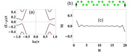
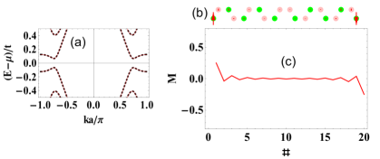
The key to understanding physical origin of the configurations AF, F and 1e is to get a deeper insight into their band structures. Obviously, low values of the conductances correspond to the situation - as illustrated in Figs. 5 and 6 for the AF configuration - with the chemical potential in the energy gap.

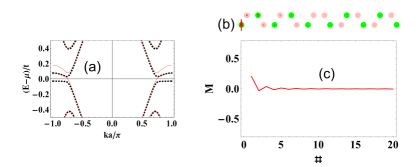
Another interesting feature seen in the phase diagram (Fig.2) is the presence of the 1-edge spin-polarized state both in graphene and in stanene. The energy band and the magnetization profile of the latter is shown in Fig. 7. These states always have strongly spin polarized conductances and are half-metallic (polarization=100%).


The magnetic moments in the panels (b) and (c) of Figs. 5-7 (and Fig. 9 below) are presented in the same scale for comparison purposes. It is easily seen that in the case of both graphene and stanene the dominating magnetic phase is the antiferromagnetic one. Moreover, with increasing this region clearly shifts to the right hand side, i.e. to higher electron occupancies.
III.3 Electrical conductance and edge magnetism of phosphorene
Like graphene, phosphorene can be obtained by mechanical exfoliation from a bulk material and also possesses high carrier mobility. However unlike graphene, phosphorene has got a natural band gap and, for instance, it can be effectively used to construct a field effect transistor Li-Yu14 . Phosphorene is a very promising material for spintronics, too. In particular, on the one hand, it has been experimentally demonstrated that magnetic moments exist at zigzag-type internal edges of porous phosphorene Nakanishi17 . On the other hand, there are many theoretical papers reporting on the importance of electronic edge states in phosphorene Ezawa15 ; Rahman17 ; Rahman17 ; Keshtan15 ; Yang16 .
It results from the Monte Carlo calculations presented in [Yang16, ] that in the case of phosphorene, narrow zigzag nanoribbons reveal a remarkable edge magnetism and for the width equal to W=6 zigzag lines, the ground state configuration at is the AF one. Analogous results have been reported in [SK18, ] for W=4 zigzag lines, and it has been shown that for W= 10, the F configuration becomes the ground state.
Figure 9 shows that a 10 zigzag lines wide phosphorene nanoribbon has the F-type magnetic arrangement for in the vicinity of . Moreover in this case the conductance is strongly spin-split and the system is half-metallic (Fig. 8), with around the chemical potential . The corresponding energy band structure and the magnetic profiles are presented in Fig.9.


The present results agree with the literature data for graphene Li14 ; Magda14 and phosphorene Nakanishi17 where the existence of the edge magnetism was experimentally demonstrated, and it was reported that hydrogenation does not destroy edge magnetism in graphene, but it does in the case of phosphorene (C is more electronegative, whereas P is slightly less electronegative than H). Noteworthy, after the oxidation the situation is reversed and graphene has no longer magnetic edges, whereas phosphorene has magnetic edges (both C and P are less electronegative than O, and p-doping takes place) Nakanishi17 ; Boukhvalov11 . Relative electronegativities determine wether n- or p-type doping comes into play, which critically modifies the dangling bonds responsible for the existence of the edge magnetic moments.
It should be also emphasized that the computed zigzag edge magnetic moments in phoshorene are considerably higher than those of graphene and stanene (cf. Fig. 9 with Figs. 5 and 6). This finding - based on the computational method which treats all the nanoribbons under consideration on equal footing - is in qualitative agreement with the experimental results of Refs. [Li14, ] and [Nakanishi17, ], reporting estimates of and up to for graphene and phosphorene, respectively. As regards stanene, to the author’s knowledge, there are not yet any experiments demonstrating that edge magnetic moments exist in zigzag nanoribbons of this type. It is to be hoped that the present results will inspire work in this direction.
IV Conclusions
In summary, by using the self-consistent tight-binding method with Hubbard correlations and spin orbit-coupling, three important atomistic structures of quasi 2D hexagonal zigzag nanoribbons have been studied, namely those with the flat (graphene), buckled (stanene) and puckered (phosphorene) atomic structures. The main focus has been directed to the transformation of electronic and magnetic properties of these materials upon doping or chemical functionalization of the zigzag edges. It has been shown that all these materials are interesting from the viewpoint of spintronic applications because graphene and stanene can have magnetic edges if n-doped, whereas in the case of phosphorene the edge magnetism can exist for the p-type doping. As shown, the edge magnetism can be effectively controlled by modification of the electron filling factors of the zigzag edge atoms, determining thereby spin-polarized electrical conductances - the essence of spintronics. Phosphorene is the most promising from this point of view because it exhibits half-metallic properties in a relatively wide energy (electron filling) range.
V References
References
- (1) E. W. Hill, A. K. Geim, K. Novoselov, F. Schedin and P. Blake, IEEE Trans. Magn. 42, 2694 (2006).
- (2) S. Krompiewski, Phys. Rev. B 80, 075433 (2009).
- (3) O. V. Yazyev, Rep. Prog. Phys. 73, 056501 (2010).
- (4) P. Seneor , B. Dlubak , M.-B. Martin , A. Anane , H. Jaffres , and A. Fert, MRS BULLETIN 37, 1245 (2012).
- (5) N. Tombros, C. Jozsa, M. Popinciuc, H. T. Jonkman and B. J. van Wees, Nature 448, 571 (2007).
- (6) M. Fujita, K. Wakabayashi, K. Nakada, and K. Kusakabe, J. Phys. Soc. Jpn. 65, 1920 (1996).
- (7) D. Soriano and J. Fernández-Rossier, Phys. Rev. B 82, 161302 (2010).
- (8) S. Krompiewski, Nanotechnology 27, 315201 (2016).
- (9) G. Z. Magda, X. Jin, I. Hagymasi, P. Vancso, Z. Osvath, P. Nemes-Incze, C. Hwang, P. P. Biro and L. Tapaszto, Nature 514, 608 (2014).
- (10) Y. Y. Li, M. X. Chen, M. Weinert and L. Li, Nat. Commun. 5, 4311 (2014).
- (11) C.-C. Liu, H. Jiang, and Y. Yao, Phys. Rev. B 84, 195430 (2011).
- (12) J. L. Lado and J. Fern ndez-Rossier, Phys. Rev. Lett. 113, 027203 (2014).
- (13) M. Ezawa, J. Phys. Soc. Jap. 84, 121003 (2015).
- (14) S. Krompiewski and G. Cunibetri, Phys. Rev. B 96, 155447 (2017).
- (15) Y. Nakanishi, A. Ishi, C. Ohata, D. Soriano, R. Iwaki, K. Nomura, M. Hasegawa, T. Nakamura, S. Katsumot, S. Roche, and J. Haruyama, Nano Res. 10, 718 (2017).
- (16) S. Krompiewski, Nanotechnology 29, 385204 (2018); ibidem, 22, 445201 (2011).
- (17) C. L. Kane and E. J. Mele, Phys. Rev. Lett. 95, 226801 (2005).
- (18) A. N. Rudenko and M. I. Katsnelson, Phys. Rev. B 89, 201408 (2014).
- (19) Wen-Chao Chen, Yuan Zhou, Shun-Li Yu, Wei-Guo Yin, and Chang-De Gong, Nano Lett. 17, 7, 4400 (2017).
- (20) Botao Fu, M. Abid, and Cheng-Cheng Liu, New J. Phys. 19, 103040 (2017).
- (21) Jingshan Qi, Kaige Hu, and Xiao Li, PHYS. REV. APPL. 10, 034048 (2018).
- (22) Fawei Zheng, Gang Zhou, Zhirong Liu, Jian Wu, Wenhui Duan, Bing-Lin Gu, and S. B. Hang, Phys. Rev. B 78, 205415 (2008).
- (23) Yi Ren, Fang Cheng, Z. H. Zhang, and Guanghui Zhou, Sci. Rep. 8, 2932 (2018).
- (24) Predrag Lazi, K. D. Belashchenko, and Igor uti, Phys. Rev. B 93, 241401 (2016).
- (25) L. Li, Y. Yu, G. J. Ye, Q. Ge, X. Ou, H. Wu, D.Feng, X. H. Chen, and Y. Zhang, Nature Nanotech. 9, 372 (2014).
- (26) M. Rahman, Ke-chao Zhou, Qing-lin Xia, Yao-zhuang Nie, and Guang-hua Guo, Phys. Chem. Chem. Phys. 19, 25319 (2017).
- (27) M. Ali M. Keshtan and M. Esmaeilzadeh, J. Phys. D: Appl. Phys. 48, 485301 (2015).
- (28) Guang Yang, Shenglong Xu, Wei Zhang, Tianxing Ma, and Congjun Wu, Phys. Rev. B 94, 075106 (2016).
- (29) D.W. Boukhvalov, Chemical Physics Letters 501, 396 (2011).