High transparency Bi2Se3 topological insulator nanoribbon Josephson junctions with low resistive noise properties
Abstract
- Abstract
-
Bi2Se3 nanoribbons, grown by catalyst-free Physical Vapour Deposition, have been used to fabricate high quality Josephson junctions with Al superconducting electrodes. The conductance spectra (dI/dV) of the junctions show clear dip-peak structures characteristic of multiple Andreev reflections. The temperature dependence of the dip-peak features reveals a highly transparent Al/Bi2Se3 topological insulator nanoribbon interface and Josephson junction barrier. This is supported by the high values of the Bi2Se3 induced gap and of IcRn (Ic critical current, Rn normal resistance of the junction) product both of the order of 160 eV, a value close to the Al gap. The devices present an extremely low relative resistance noise below 110-12 m2/Hz comparable to the best Al tunnel junctions, which indicates a high stability in the transmission coefficients of transport channels. The ideal Al/Bi2Se3 interface properties, perfect transparency for Cooper pair transport in conjunction with low resistive noise make these junctions a suitable platform for further studies of the induced topological superconductivity and Majorana bound states physics.
The interest for hybrid Topological Insulator (TI) Josephson junctions has boosted after the prediction by Fu and Kane Fu2008 of an unconventional chiral px + py (p-wave) symmetry of the proximity induced order parameter into the topological surface states. The chiral induced p-wave is a prerequisite for the nucleation of localized Majorana states in a tri-junction geometry Fu2008 which are instrumental for topological quantum computation. In a multimode hybrid TI Josephson junction, with two terminal geometry, Majorana physics manifests as peculiar properties of a part of the Andreev bound states carrying the Josephson current: they give rise to an unconventional 4 periodic current phase relation (CPR) coexisting with a 2 periodic CPR of the conventional Andreev bound states Wiedenmann2016 . The relative weight between the 4 and 2 periodic Andreev bound states increases with the transparency of the junction and in general by reducing the number of channelsSnelder2013 ; Li2018a . A direct way to achieve a low number of transport channels is to use TI with reduced dimensionality like very thin and narrow nanoribbons. Indeed quite recently, various theoretical proposals have shown the advantage to use Josephson junctions with TI nanoribbon, with suppressed bulk conduction, to realize Majorana fermions Manousakis2017 .
In this letter we demonstrate the realization of Bi2Se3 nanoribbon Josephson junctions with Al electrodes with a) highly transparent Bi2Se3/Al interface, b) highly transparent barrier for Cooper pair transport and c) low resistance noise. The combination of all these properties are instrumental to study novel effects related to topological superconductivity.
As already observed in Josephson devices made with 2-dimensional electron gases (2DEG) Chrestin1997 ; Kjaergaard2017 , the detection of Multiple Andreev Reflections (MAR) is a powerful tool to get information about the value of the induced gap and insights into the Cooper pair transport. In situ growth of the superconducting electrodes on the 3D TI would be the ideal strategy to realize highly transparent Superconductor / 3D TI interfaces as demonstrated in the case of InAs nanowires and 2DEG Chang2015 ; Kjaergaard2017 . However at present, most of the results presented in literature, on the induced superconductivity in 3D TI’s, refer to devices fabricated from flakes, exfoliated from single crystals or films, and then transferred to a substrate Cho2013 ; Galletti2014 ; Calvez2018 . In this case the interfaces with the superconductor are realized ex-situ after the removal of the oxide layer which unavoidably form on top of the 3D TI Kong2011a .
Here we report an excellent coupling between Bi2Se3 nanoribbons and Al, by using an ex-situ procedure for the definition of the interface. Differential conductance spectra display sub-gap structures resulting from MAR.
The as grown nanoribbons Andzane2015a ; Kunakova2018 were transferred to SiO2 (300nm)/Si substrates and electron beam lithography processing was used to define the electrodes separated by a distance ranging from 70 nm to 150 nm. Prior to the deposition of the electrodes the Bi2Se3 nanoribbon is etched by Ar+ ion milling to remove the layer of native oxide. This step is followed by the evaporation of the bilayer Pt and Al (3nm/80nm). In our earlier works Galletti2014 ; Galletti2014a ; Galletti2017 ; Charpentier2017 , by using TI flakes, we have demonstrated the crucial role of Pt to create a transparent interface when Al is employed as electrode. This has been also confirmed by other authors Ghatak2018a . All the measurements presented here were conducted in an -filtered dilution refrigerator with a base temperature of 19 mK.
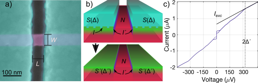
Fig. 1a shows a Scanning Electron Microscope (SEM) image of one of the fabricated planar Josephson junctions of Al/Bi2Se3/Al. Ideally, a planar Josephson junction can be described as SIS′I′-N-I′S′IS (see schematics in Fig. 1b). Here S′ is the proximized TI (under the superconducting electrode S), characterized by an induced gap while N is the part of the TI in the nanogap not covered by the superconductor (Fig. 1b). I indicates the barrier between the Al and the Bi2Se3 nanoribbon while I′ is the barrier between the Bi2Se3 under the Al and that Bi2Se3 in the nanogap.
The current-voltage characteristic (IVC) of one of the nanoribbon Josephson junctions is shown in Fig. 1c. The IVCs of our junctions typically display a hysteretic behaviour which is an indication of an increased electron temperature once the junction switches to the resistive state Courtois2008 . The switching current Ic is determined from the forward sweep, and for the junction B45-C1 Ic is 0.20 A (Table S1, in Supplementary Information (SI)). This corresponds to a current density Jc of 2.9103 A/cm2. The value of the current density is comparable to other previously reported 3D TI Josephson junctions with much larger cross sectionsGalletti2014a ; Stehno2016 .
An important figure of merit of a Josephson junction is the characteristic voltage or IcRN product. The normal state resistance RN can be extracted from the inverse of the slope of the IVC at voltages above 2 (320 eV). For the junction B45-C1, RN of 330 yields IcRN = 66 eV (Table S1, SI). The IcRN increases to about 170 eV as increasing the width of the nanoribbon by a factor of two (see in Table S1, SI).
A common feature for all the investigated devices is the presence of an excess current (Iexc) in the IVC, which occurs due to Andreev reflection. Iexc is obtained by extrapolating the linear part of the IVC, taken at voltages much higher than the gap of Al (see Fig. 1c), to V = 0. In the theoretical model first developed by Blonder, Tinkham and Klapwijk and later on modified by Flensberg,Flensberg1988 the transparency of the barrier I′ in a S′I′NI′S′ junction can be related to dimensionless parameter Z which give the strength of barrier: one gets that = 1/(1 + Z2). The transparency is then connected to the value of the excess current through the quantity eIexcRN/, where RN is the resistance of the normal state.
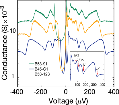
In Fig. 2a we show the conductance spectra of some of the measured devices with slightly different geometrical parameters (L) (w) (t), (Table S1, SI). The conductance spectra for all the junctions exhibit clear features at voltages below the gap of Al. In case of a very high transparency of the Josephson junction, the dips in the conductance spectra are associated to Multiple Andreev Reflections, occurring at voltages V=2/en, where n is an integer Kleinsasser1994 ; Averin1995 . Fig. 2b depicts the enlarged conductance spectra for device B45-C1. The red arrows indicate the positions of the dips, that follow the relation 2/en. The induced gap for this junction is found to be 168 eV (Table S1, SI). This value of the induced gap can be used to evaluate the transparency , which for all junctions is found in the range 0.65 - 0.85, indicating a good transmission through the barrier I′ (see Fig. 1b). It is important to note, that such high transparency of the Josephson barrier interface is reproducible from nanoribbon to nanoribbon (Table S1, SI).
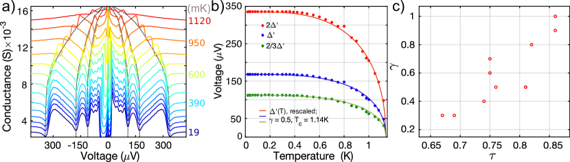
Fig. 3a illustrates the conductance spectra for device B45-C1 measured at different temperatures. The temperature dependence of the induced gap can be described as Aminov1996 ; Chrestin1997 :
| (1) |
Here the parameter is proportional to the ratio where and are respectively the resistivity and the coherence length of the Bi2Se3 and the interface resistivity between Al and Bi2Se3.
The three main conductance dips that we observe (n = 1, 2, 3) are identified as 2, and 2/3. They are plotted as a function of the temperature (Fig. 3b) and can be well approximated using equation 1. We find the best fit of the data (T) to eq. 1 by using = 0.5 and the critical temperature of the junction Tc = 1.14 K. The other two curves of the fit for the temperature dependence of the conductance dips 2(T) and 2/3(T) (red and green solid lines in Fig. 3b) are obtained by rescaling to the (T) values (multiplying by 2 and 2/3 respectively) and keeping the same parameters of Tc and . The good fitting of the 2/n curves to eq. 1 supports the assumption that the dips in the conductance spectra are due to the proximity induced superconducting gap in the Bi2Se3.
Fig. 3c shows the dependence of the extracted values, for the junctions reported in Table S1, as a function of the transparency of the barrier I′ (extracted from Iexc Flensberg1988 ).
Quite surprisingly the lowest values of correspond to the lowest value of meaning the transparency of the barrier I′ is reduced by reducing the ratio , which corresponds to a larger value of the induces gap . This behaviour can be understood considering that the Al electrode material is also doping the Bi2Se3 underneath. A change in the transparency of the Al/Bi2Se3 interface (variation of ) produces a change in the Bi2Se3 material, through doping, which modifies the product as well. Our measurements show that the reduction in does not reflect in an equal reduction of the product, otherwise we would have not detected an increase in . The “response” of the product to variation of will depend on the initial doping of the material and it can eventually be tuned by gating. The improved coupling between the Al and the Bi2Se3 leads to a more doped TI underneath the electrodes, which naturally causes a difference between the chemical potentials of the Bi2Se3 doped by the Al electrodes compared to the Bi2Se3 in the nanogap. The resulting Fermi momentum mismatch leads to an effective barrier I′, which will be more or less transparent depending on the extrinsic doping level difference (coming from the Al electrodes) in the two Bi2Se3 regions.
While high transparent Bi2Se3 / Al interfaces are instrumental to get high values of the induced gap important for high working temperature of the device, this happens at the expenses of the transparency of the interface I′ which affects the visibility of the (Majorana) Andreev bound states leading to a 4 periodic CPR. Indeed the number of modes leading to a 4 periodic CPR increases for higher values of the transparency of the barrier I′ Snelder2013 ; Li2018a . A precise control of the interface between the Al and the Bi2Se3 is therefore important to reach values of higher than 0.85 achieved in this work.
To further corroborate the quality of our 3D TI junctions we have performed low frequency resistance noise measurements at voltages above 2/e. The resistance fluctuations R are measured by applying a constant bias current and recording the voltage fluctuations as a function of time V(t) = R(t) Ib. The time dependent voltage signal is then amplified by a room temperature low noise amplifier and the output sent to an FFT spectrum analyser. The amplifier noise contribution was further reduced by using two amplifiers in parallel and performing a cross-correlation spectrum in the FFT analyserArpaia2016 .
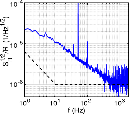
In Fig. 4 we show the normalized resistance noise power spectral density, S/R = /R, of junction B45-32 measured at T = 500 mK. At frequencies below 1 kHz we clearly observe the typical 1/ dependence of resistance noise common to solid state electronic systems Kogan1996 . Resistance fluctuations can be attributed to fluctuations of the transmission coefficients of the transport modes or the number of transport modes on the TI surface. An empirical equation for 1/ resistance noise is given by Hooge’s expression for low frequency voltage noise SV/V2 = SR/R2 = /(), where is the frequency, is the carrier density, is the surface area of the TI between the superconducting electrodes, and is the Hooge’s parameter, which is a measure for the ”noisiness” of the system. Using a typical total carrier concentration of 11013 cm-2 for our nanoribbons Kunakova2018 we obtain a Hooge’s parameter = 710-7. We have measured low frequency noise on 3 more TI junctions, which resulted in a Hooge’s parameter in the range 5 910-7. These values are 3 to 4 orders of magnitude lower than those reported in literature on Bi based TI junctions measured at T = 4 7 K Zhang2016 ; Bhattacharyya2015 . The low noise values can be attributed to the quasi ballistic limit of our 3D TI junctions and the very clean interfaces in our devices resulting in low fluctuations of the transport mode transmission coefficients.
To identify the microscopic origin of the resistance noise observed in our 3D TI junctions a detailed study of noise as a function of temperature and external gate voltage will be required Zhang2016 ; Bhattacharyya2015 . However, this is beyond the scope of this paper. Resistance noise in a Josephson junction gives a lower bound for critical current noise, which is a source of dephasing in Josephson junction based superconducting qubits VanHarlingen2004 . For experiments aiming at detecting Majorana zero energy modes in TI Josephson junctions embedded in circuit quantum electrodynamics architectures Ginossar2014 qubit we compare the resistance noise of our TI junctions to Al tunnel junctions employed in state of the art Josephson junction qubit architectures. Typical reported values of the relative resistance noise at 1 Hz multiplied by the junction area AJ (perpendicular to the transport current), i.e. AJSR/R2, are in the range 210-14 2 10-13 m2/Hz Eroms2006a ; Nugroho2013 . For our junctions we obtain values in the range 310-13 1 10-12 m2/Hz, which are close to the best reported values for Al tunnel junctions.
In conclusion we have realized low noise and high transparency 3D TI nanoribbon Josephson junctions instrumental to study topological superconductivity in few modes devices.
Acknowledgements
This work has been supported by the European Union’s Horizon 2020 research and innovation programme (grant agreement No. 766714/HiTIMe). G.K. acknowledges European Regional Development Fund project No 1.1.1.2/VIAA/1/16/198.
Supplementary Information
See Supplementary Information (SI) for physical parameters of the studied junctions, extraction of the induced gap from conductance vs voltage measurements, and resistance vs. temperature measurements of a junction.
References
- (1) L. Fu and C. L. Kane, “Superconducting proximity effect and majorana fermions at the surface of a topological insulator”, Physical Review Letters 100, 096407 (2008).
- (2) J. Wiedenmann, E. Bocquillon, R. S. Deacon, S. Hartinger, O. Herrmann, T. M. Klapwijk, L. Maier, C. Ames, C. Brune, C. Gould, A. Oiwa, K. Ishibashi, S. Tarucha, H. Buhmann, and L. W. Molenkamp, “4-periodic Josephson supercurrent in HgTe-based topological Josephson junctions”, Nature Communications 7, 10303 (2016).
- (3) M. Snelder, M. Veldhorst, A. A. Golubov, and A. Brinkman, “Andreev bound states and current-phase relations in three - dimensional topological insulators”, Physical Review B - Condensed Matter and Materials Physics 87, 1–7 (2013).
- (4) C. Li, J. C. de Boer, B. de Ronde, S. V. Ramankutty, E. van Heumen, Y. Huang, A. de Visser, A. A. Golubov, M. S. Golden, and A. Brinkman, “4-periodic Andreev bound states in a Dirac semimetal”, Nature Materials 17, 875–880 (2018).
- (5) J. Manousakis, A. Altland, D. Bagrets, R. Egger, and Y. Ando, “Majorana qubits in a topological insulator nanoribbon architecture”, Physical Review B - Condensed Matter and Materials Physics 95, 165424 (2017).
- (6) A. Chrestin, T. Matsuyama, and U. Merkt, “Evidence for a proximity-induced energy gap in Nb / InAs / Nb junctions”, Physical Review B - Condensed Matter and Materials Physics 55, 8457–8465 (1997).
- (7) M. Kjaergaard, H. J. Suominen, M. P. Nowak, A. R. Akhmerov, J. Shabani, C. J. Palmstrm, F. Nichele, and C. M. Marcus, “Transparent Semiconductor-Superconductor Interface and Induced Gap in an Epitaxial Heterostructure Josephson Junction”, Phys. Rev. Appl., 034029 (2017).
- (8) W. Chang, S. M. Albrecht, T. S. Jespersen, F. Kuemmeth, P. Krogstrup, J. Nygård, and C. M. Marcus, “Hard gap in epitaxial semiconductor-superconductor nanowires”, Nature Nanotechnology 10, 232–236 (2015).
- (9) S. Cho, B. Dellabetta, A. Yang, J. Schneeloch, Z. Xu, T. Valla, G. Gu, M. J. Gilbert, and N. Mason, “Symmetry protected Josephson supercurrents in three-dimensional topological insulators”, Nature Communications 4, 1686–1689 (2013).
- (10) L. Galletti, S. Charpentier, M. Iavarone, P. Lucignano, D. Massarotti, R. Arpaia, Y. Suzuki, K. Kadowaki, T. Bauch, A. Tagliacozzo, F. Tafuri, and F. Lombardi, “Influence of topological edge states on the properties of Al/Bi2Se3/Al hybrid Josephson devices”, Physical Review B - Condensed Matter and Materials Physics 89, 134512–9 (2014).
- (11) K. L. Calvez, L. Veyrat, F. Gay, P. Plaindoux, C. Winkelmann, H. Courtois, and B. Sacèpè, “Joule overheating poisons the fractional ac Josephson effect in topological Josephson junctions”, Communications Physics , 1–9 (2018).
- (12) D. Kong, J. J. Cha, K. Lai, H. Peng, J. G. Analytis, S. Meister, Y. Chen, H. J. Zhang, I. R. Fisher, Z. X. Shen, and Y. Cui, “Rapid surface oxidation as a source of surface degradation factor for Bi2Se3”, ACS Nano 5, 4698–4703 (2011).
- (13) J. Andzane, G. Kunakova, S. Charpentier, V. Hrkac, L. Kienle, M. Baitimirova, T. Bauch, F. Lombardi, and D. Erts, “Catalyst-free vapour-solid technique for deposition of Bi2Te3 and Bi2Se3 nanowires/nanobelts with topological insulator properties”, Nanoscale 7, 15935 (2015).
- (14) G. Kunakova, L. Galletti, S. Charpentier, J. Andzane, D. Erts, F. Lèonard, C. D. Spataru, T. Bauch, and F. Lombardi, “Bulk- Free Topological Insulator Bi2Se3 nanoribbons with Magnetotransport Signatures of Dirac Surface States”, Nanoscale 10, 19595–19602 (2018).
- (15) L. Galletti, S. Charpentier, P. Lucignano, D. Massarotti, R. Arpaia, F. Tafuri, T. Bauch, Y. Suzuki, A. Tagliacozzo, K. Kadowaki, and F. Lombardi, “Josephson effect in Al/Bi2Se3/Al coplanar hybrid devices”, Physica C: Superconductivity 503, 162–165 (2014).
- (16) L. Galletti, S. Charpentier, Y. Song, D. Golubev, S. M. Wang, T. Bauch, and F. Lombardi, “High-Transparency Al/Bi2Te3 Double-Barrier Heterostructures”, IEEE Transactions on Applied Superconductivity 27, 1800404–4 (2017).
- (17) S. Charpentier, L. Galletti, G. Kunakova, R. Arpaia, Y. Song, R. Baghdadi, S. M. Wang, A. Kalaboukhov, E. Olsson, F. Tafuri, D. Golubev, J. Linder, T. Bauch, and F. Lombardi, “Induced unconventional superconductivity on the surface states of Bi2Te3 topological insulator”, Nature Communications 8, 2019 (2017).
- (18) S. Ghatak, O. Breunig, F. Yang, Z. Wang, A. A. Taskin, and Y. Ando, “Anomalous Fraunhofer Patterns in Gated Josephson Junctions Based on the Bulk-Insulating Topological Insulator BiSbTeSe2”, Nano Letters 18, 5124–5131 (2018).
- (19) H. Courtois, M. Meschke, J. T. Peltonen, and J. P. Pekola, “Origin of hysteresis in a proximity Josephson junction”, Physical Review Letters 101, 1–4 (2008).
- (20) M. P. Stehno, V. Orlyanchik, C. D. Nugroho, P. Ghaemi, M. Brahlek, N. Koirala, S. Oh, and D. J. Van Harlingen, “Signature of a topological phase transition in the Josephson supercurrent through a topological insulator”, Physical Review B - Condensed Matter and Materials Physics 93, 1–10 (2016).
- (21) K. Flensberg, J. B. Hansen, and M. Octavio, “Subharmonic energy gap structure in superconducting weak links”, Physical Review B - Condensed Matter and Materials Physics 38, 8707– 8711 (1988).
- (22) A. W. Kleinsasser, R. E. Miller, W. H. Mallison, and G. B. Arnold, “Observation of Multiple Andreev Reflections in Superconducting Tunnel Junctions”, Physical Review Letters 72, 1738–4 (1994).
- (23) D. Averin and A. Bardas, “ac Josephson effect in a single quantum channel”, Physical Review Letters 75, 1831–1834 (1995).
- (24) B. A. Aminov, A. A. Golubov, and M. Y. Kupriyanov, “Quasiparticle current in ballistic constrictions with finite transparencies of interfaces”, Phys. Rev. B 53, 365–373 (1996).
- (25) R. Arpaia, M. Arzeo, S. Nawaz, S. Charpentier, F. Lombardi, and T. Bauch, “Ultra low noise YBa2Cu3O7-δ nano superconducting quantum interference devices implementing nanowires”, Applied Physics Letters 252601, 072603–4 (2016).
- (26) S. Kogan, Electronic Noise and Fluctuations in Solids, Cambridge University Press, Cambridge, 1996.
- (27) H. Zhang, Z.-J. Song, J.-Y. Feng, Z.-Q. Ji, and L. Lu, “Low Frequency Noise in Gate Tunable Topological Insulator Nanowire Field Emission Transistor near the Dirac Point”, Chinese Physics Letters 33, 087302 (2016).
- (28) S. Bhattacharyya, M. Banerjee, H. Nhalil, S. Islam, C. Dasgupta, S. Elizabeth, and A. Ghosh, “Bulk-Induced 1/f Noise at the Surface of Three-Dimensional Topological Insulators”, ACS Nano 9, 12529–12536 (2015).
- (29) D. J. Van Harlingen, T. L. Robertson, B. L. T. Plourde, P. A. Reichardt, T. A. Crane, and J. Clarke, “Decoherence in josephson junction qubits due to critical current fluctuations”, Phys. Rev. B 70, 064517 (2004).
- (30) E. Ginossar and E. Grosfeld, “Microwave transitions as a signature of coherent parity mixing effects in the majorana transmon qubit”, Nature Communications 5, 4772 (2014).
- (31) J. Eroms, L. C. van Schaarenburg, E. F. C. Driessen, J. H. Plantenberg, C. M. Huizinga, R. N. Schouten, A. H. Verbruggen, C. J. P. M. Harmans, and J. E. Mooij, “Low-frequency noise in Josephson junctions for superconducting qubits”, Applied Physics Letters 89, 122516 (2006).
- (32) C. D. Nugroho, V. Orlyanchik, and D. J. Van Harlingen, “Low frequency resistance and critical current fluctuations in Al-based Josephson junctions”, Applied Physics Letters 102, 142602 (2013).