Ultrafast sensing of photoconductivity decay using microwave resonators
Abstract
Microwave reflectance probed photoconductivity (or -PCD) measurement represents a contactless and non-invasive method to characterize impurity content in semiconductors. Major drawbacks of the method include a difficult separation of reflectance due to dielectric and conduction effects and that the -PCD signal is prohibitively weak for highly conducting samples. Both of these limitations could be tackled with the use of microwave resonators due to the well-known sensitivity of resonator parameters to minute changes in the material properties combined with a null measurement. A general misconception is that time resolution of resonator measurements is limited beyond their bandwidth by the readout electronics response time. While it is true for conventional resonator measurements, such as those employing a frequency sweep, we present a time-resolved resonator parameter readout method which overcomes these limitations and allows measurement of complex material parameters and to enhance -PCD signals with the ultimate time resolution limit being the resonator time constant. This is achieved by detecting the transient response of microwave resonators on the timescale of a few 100 ns during the -PCD decay signal. The method employs a high-stability oscillator working with a fixed frequency which results in a stable and highly accurate measurement.
I Introduction
Microwave detected photoconductivity measurement, -PCD Ohsawa et al. (1983); Kunst and Beck (1986); Lauer et al. (2008), is a standard laboratory and industrial tool to characterize the amount of light-excited charge carriers and their lifetime. Knowledge of these parameters is crucial for semiconductor applications in light harvesting and also for the characterization of impurity concentrations. Examples include the characterization of Co and Fe impurities in silicon wafers Lauer et al. (2008); Berger et al. (2011), the light-induced carrier recombination rate measurements in novel perovskite based photovoltaic materials Chouhan et al. (2017); Labram and Chabinyc (2017); Guse et al. (2016); Bi et al. (2016), non-silicon semiconductors, e.g. CdSe and CdTe (Ref. Novikov et al., 2010) and novel low-dimensional materials including carbon nanotubes Freitag et al. (2003); Lu and Panchapakesan (2006), graphene Vasko and Ryzhii (2008); Docherty et al. (2012), transition metal dichalcogenides Xia et al. (2014), and black phosphorus Liu et al. (2016); Miao et al. (2017).
The most conventional -PCD implementations rely on detecting reflection of microwaves from a sample which is irradiated using an antenna or an open waveguide, i.e. by non-resonant means. Besides its simplicity, this approach usually suffers from a large, non light-induced reflected background signal that can either saturate the receiver electronics (thus preventing measurement of small light-induced reflections) or perplex the phase sensitive analysis of the back-reflected microwave signal. Measurement of the phase is required in order to separate the reflection due to dielectric and conduction effects. This hindrance is especially pronounced for samples with a high conductivity, i.e. for a doped semiconductor.
It was recognized back in 1977 (Refs. Infelta et al., 1977; Fessenden et al., 1982) and reiterated recently (Ref. Reid et al., 2017) that the use of microwave resonators could eliminate the above mentioned problems since resonators allow for a null measurement and also to improve the sensitivity of the method due to the well-known amplifying effect of resonators. The latter can be best demonstrated for considering a single resistor with resistance whose value changes by . In case the resistor is part of a high quality factor () RLC circuit, whose impedance is matched to a waveguide with wave-impedance of (), the change of the return impedance near the resonance frequency of the resonator is (Ref. Pozar, 2004), i.e. the sensitivity to a small resistance change is significantly enhanced (we present a lumped element circuit model calculation in the Supplementary Materials). Equivalently, it is often expressed as (Ref. Cetinoneri et al., 2010).
The known approach to combine the -PCD measurement with microwave resonators involves the detection of power reflected from a resonator during and after a light pulse Subramanian et al. (1998); Novikov et al. (2010). However, this method ignores the information contained in the phase (due to the power detection). In addition, both frequency and -factor changes lead to a modified reflection, thus modeling to obtain material dependent parameters is rather involved Amato (1982); Fessenden et al. (1982); Eckstrom et al. (1987). Nevertheless, the approach yields effective -PCD lifetime values and it was successful in constructing sensitive electromagnetic radiation detectors Kessick et al. (2000); Tepper and Losee (2001); Cetinoneri et al. (2010); Braggio et al. (2014).
Clearly, a modeling-independent, time-resolved measurement of resonator and eigenfrequency, , is highly desired. It is well known that the finite bandwidth of resonators inherently limits time-resolved measurements to the resonator time constant of , with typical values of for and . However, an additional misconception is that the practical measurement of the factor and is limited further to a few ms or even seconds, depending on the analyzing electronics in a frequency swept experiment using e.g. a network analyzer Petersan and Anlage (1998); Luiten (2005); Kajfez (2005). This is prohibitively slow for a meaningful time-resolved resonator measurement.
We recently reported a novel method Gyüre et al. (2015); Gyüre-Garami et al. (2018) which allows measurement of the resonator parameters, and , with a rapid time domain measurement. The technique shows great resemblance to pulsed nuclear magnetic resonance methods Ernst (1992) and to the optical cavity ring-down spectroscopy Hodges et al. (2004); Hodges and Ciurylo (2005); Cygan et al. (2011); Truong et al. (2013). The pulsed resonator readout method employs a short RF pulse with carrier frequency not necessarily matching () which induces both a switch-on and switch-off transients. Both transients represent a decaying oscillation on the eigenfrequency of the resonator, (Ref. Schmitt and Zimmer, 1966) and with its time constant, (Refs. Gallagher, 1979; Komachi and Tanaka, 1974; Amato, 1982; Quine et al., 2011). The transient signals can be conveniently downconverted with the same frequency as the exciting signal. Such measurements in the time domain have two important advantages: enhanced accuracy (also known as the Connes advantage Connes and Connes (1966)) since the measurement is traced back to a stable frequency, and a simultaneous measurement of the whole resonator response (also known as Fellgett or multiplex advantage Fellgett (1949)).
This time-resolved, pulsed resonator readout method has been successfully employed to evidence a heating related microwave absorption anomaly in carbon nanotubes G. Márkus et al. (2018) and to improve the measurement accuracy of power absorbed from an RF field in magnetic ferrite nanoparticles during hyperthermia Gresits et al. (2019). These results motivate the present study to explore the possibility to use this method for the detection of time-resolved -PCD studies in silicon. Herein, we report time-resolved -PCD measurements for a silicon single crystal samples which are placed inside a microwave cavity resonator with a time constant of about 100 ns. A Q-switch laser induces extra electron-hole pairs in the sample and the laser repetition is synchronized with a train of short microwave pulses. The resulting switch-off transient is detected after each microwave pulse, which yields information about the sample photoconductivity. We present time-resolved resonator and data on a silicon wafer sample with -PCD lifetime around 100 s. The measurement clearly demonstrates the utility of the pulsed resonator readout method for the detection of time-resolved microwave detected photoconductivity measurements.
II Principle of the -PCD measurements
II.1 The conventional -PCD method
In order to illustrate the advances of the present method, we recapture the principle of the conventional -PCD studies. The conventional -PCD method is based on detecting the reflection of microwaves from a semiconductor wafer. Reflection of electromagnetic waves from a material can be most conveniently described with the introduction of the wave impedance of the materialPozar (2004); Chen et al. (2004):
| (1) |
where is the permeability, is the permittivity, is the angular frequency of the wave, and is the conductivity of the sample. In general, , , and are complex quantities. Note that Eq. (1) returns the well-known wave impedance of vacuum for and . For conductors, is denoted by the surface impedance, , which highlights that electromagnetic waves penetrate only into the surface of metals. Then ( finite, ) and within the quasi-stationary approximation (), the above formula for returns the well-known expression for the surface impedance of , where the penetration depth reads: . It also implicitly contains the often used complex dielectric constant for a lossy dielectric (i.e. a dielectric with a finite ): ( is the real dielectric constant of the material).
We then consider that the material occupies the half space and it has a surface impedance of . An electromagnetic wave interacts with it, which propagates in free space or in a generic waveguide (it could be a coaxial cable or a TE10 microwave waveguide) thus this medium is modeled with a wave impedance of . The radiation is reflected from the material and the reflection coefficient (i.e. ratio of the transmitted to reflected field voltage or amplitude), , is given as Pozar (2004):
| (2) |
In the so-called parameter representation, holds (the equality is strictly valid for zero transmission, see Ref. Chen et al., 2004, p. 196). For a -PCD experiment in an industrial environment, the reflection is often detected by an antenna, which induces additional geometric factors but it does not affect the generic physical description in Eq. (2).
Eq. (2) is related to the usual Fresnel reflection formula of (for normal incidence of electromagnetic waves from vacuum, ) by recognizing the relation between the wave impedance and the index of refraction as: . The complex index of refraction for a non-magnetic material reads .
Alternatively for good conductors, the reflection at low frequencies can be approximated with the Hagen-Rubens relation:
| (3) |
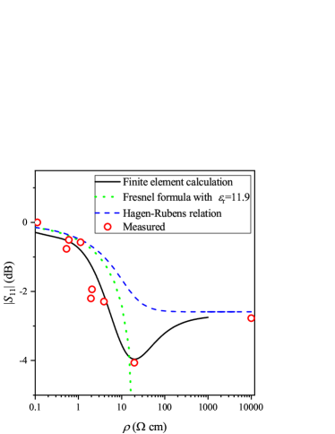
The reflection amplitude, , from a silicon single crystal wafer with varying resistivity is shown in Fig. 1 for various approximations: a finite element electromagnetic modeling for the wafer covering a WR90 X-band waveguide (TE10 mode, 8-12.4 GHz), the Fresnel formula, the Hagen-Rubens relation. We found that the calculated reflections are little affected when we considered the small variation of as a function of doping, according to Ref. Ristic et al., 2004. The figure demonstrates that the Hagen-Rubens relation falls well onto the other two calculations in its domain of validity.
Fig. 1. also contains the experimental results. To obtain these, we covered the WR90 X-band waveguide with a series of silicon single crystal wafers with varying resistivity from up to , i.e. through 4 orders of magnitude in . We used a copper plate covering the waveguide as reference. As expected, the experimental data lies close to the result of the finite element electromagnetic modeling. The Fresnel formula also demonstrates well the general trend in the reflected amplitude, even if it deviates from the electromagnetic modelling.
In principle, the reflection approach allows to determine the real and imaginary parts of the material parameters from the phase sensitive detection of the reflected microwaves. However, this measurement requires an accurate calibration of the reflected microwave phase. In addition, most -PCD measurements, which are implemented in an industrial environment, measure the reflected microwave power only. In contrast, as we shall show below, a measurement of the material parameters in a microwave resonator allows for the automatic disentanglement of the real and imaginary parts of the material parameters.
Nevertheless, the major hindrance of the conventional -PCD method is that a substantial reflection is present already in dark conditions: as Fig. 1. shows, for most cases the reflection is around 3 dB, i.e. half of the microwave power is reflected even without illumination. It clearly hinders the detection of the extra, light-induced reflection by the saturation of the detecting electronics and the always present dark background gives rise to additional shot noise.
II.2 The resonator based -PCD method
The so-called cavity perturbation method Buravov and Shchegolev (1971); Klein et al. (1993) is applicable for a sample which is placed inside a microwave cavity resonator. The presence of the sample affects both the resonance frequency, , and quality factor, , of the unloaded resonator. It was derived in Ref. Landau and Lifschitz, 1984 that the resonator perturbation for a cylinder with diameter reads:
| (4) |
where is a sample size dependent constant (also depends on the cavity mode and electromagnetic field distribution). is the shift in the resonant frequency and is the additional, sample related loss in the cavity. The authors of Ref. Landau and Lifschitz, 1984 introduced the polarizability:
| (5) |
with being the complex wavenumber of the microwaves inside the material. and are Bessel functions of the first kind.
In the limit of finite electromagnetic wave penetration into the sample, Eq. (4) reduces to the better known expression which relates the resonator parameters directly to the surface impedance according to Eq. (1), as follows Pozar (2004); Chen et al. (2004); Klein et al. (1993); Donovan et al. (1993); Dressel et al. (1993):
| (6) |
where is a geometry factor (not dimensionless) that is proportional to the ratio of the sample surface to the cavity surface but it also depends on the resonator mode. We discuss an additional sample geometry and explicitly derive the relation between Eqs. (4) and (6) in the Supplementary Materials.
Eq. (4) shows that measurement of the cavity frequency shift and loss allows to disentangle the real and imaginary parts of the material wave impedance. A limitation of the method is that the geometry factor is generally unknown therefore a calibrating measurement is required to obtain absolute material parameter values. The resonator based method prevails when the relative changes in the material parameter is required as a function of time.
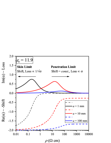
Fig. 2. summarizes the change of a microwave resonator parameters for a sample with varying resistivity according to Eq. (4) with the for silicon. The behavior can be split to two regimes depending on whether the microwaves penetrate into the sample (penetration limit) or whether it is limited by the skin-effect. For the earlier, the shift is constant and the loss, , is linear to . In the latter, the skin limit, the real and imaginary parts of are equal and are both proportional to . This correspondence allows to obtain the material parameters from the measurement of the cavity, besides the geometry factor. However, the major advantage of using the microwave resonators is the essentially null measurement it provides.
We emphasize that Eq. (4) gives the cavity perturbation formula for an arbitrary value of and . Often one discusses the two extremal cases for the cavity perturbation only: e.g. for -PCD studies on gas or liquid plasmas Infelta et al. (1977) or on materials with a low conductivity Subramanian et al. (1998) the penetration limit is discussed only, whereas the skin-limit with the surface impedance description is used for good conductors Klein et al. (1994). While the full analysis of and can be performed for the case of cavity perturbation, this is beyond the scope of the present contribution and we focus on the technical development, i.e. on the time-resolved measurement of the resonator shift and loss.
III The resonator based photoconductivity measurement
III.1 The measurement setup
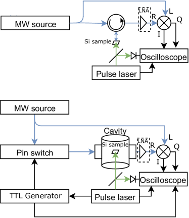
Our setup for the time-resolved -PCD measurement is shown in Fig. 3 including both the conventional (upper panel) and the novel, resonator based approach (lower panel). A Q-switch pulse laser (527 nm Coherent Evolution-15, Nd:YLF) with 1 kHz repetition frequency and pulse duration is used for the excitation of charge carriers in the semiconductor samples. We note that the 527 nm excitation is capable of photoexciting charge carriers in silicon, even though its band edge is around 1100 nm, which would be a more efficient wavelength for such purposes.
The microwave source is a PLL locked synthesizer (HP-Agilent 83751B or a Kühne Electronic GmbH model MKU LO 8-13 PLL) which drives the LO of an IQ mixer (Marki Microwave IQ0618LXP double-balanced mixer, LO/RF: 6-18 GHz, IF: DC-500 MHz, 7.5 dB conversion loss). The mixer downconverts the incoming RF signal and the I and Q signals are digitized with an oscilloscope (Tektronix MDO-3024, BW=200 MHz).
Optionally, the RF signal can be amplified by a low noise amplifier (LNA, JaniLab Inc., NF=1.4 dB, Gain=15 dB, 1 dB compression point, P1dB, 10 dBm), which is indicated by a dashed box in the figure. Both the LO and RF inputs of the mixer are isolated galvanically from the rest of the circuit with band-pass (8-12 GHz) DC-blocks. The rising edge of the laser pulses are detected with a fast photodiode (Thorlabs DET36A/M) which provides a jitter-free trigger signal.
This signal triggers the oscilloscope in the conventional setup: therein a standard X-band (8-12.4 GHz) WR90 waveguide is used to irradiate samples. The silicon wafers fully cover the waveguide and are illuminated by the light, whose beam aperture is such that it roughly covers the entire waveguide opening. We checked that the laser illumination from the front (i.e. opposite to the microwave irradiation direction) gives qualitatively identical results to those when the sample is irradiated from the back (i.e. parallel to the microwave irradiation direction). The only difference is that irradiation from the back results in smaller signals as the microwave waveguide limits the insertion of light. A standard X-band circulator (Ditom Microwave Inc.) acts as duplexing unit between the exciting and reflected microwaves.
In the novel setup, the sample is inside a microwave cavity resonator operating in the TE011 mode (with an unloaded quality factor ) and we use it in transmission. The cavity is undercoupled for both the input and output () which represents a compromise between the resonator bandwidth and transmitted signal Pozar (2004). The parameters of the resonator are measured with the transient method Gyüre et al. (2015); Gyüre-Garami et al. (2018): the exciting microwaves are pulsed, which forces the cavity to transmit microwaves in a transient state. Although the exciting carrier frequency, , does not necessarily match the resonator eigenfrequency, still the transient signal oscillates on the resonant frequency of the cavity, . The carrier of the excitation frequency, , is intentionally detuned from in order to detect the transient with an intermediate frequency around MHz, which removes the 1/ noise of the mixer.
The microwave pulses are formed with a fast PIN diode switch (Advanced Technical Materials, S1517D, 5 ns 10-90% rise-fall transient) which is driven by a TTL signal. This signal contains a switch-on of 0.5 s and is repeated every 2 s. This duration and repetition are well suited for our cavity with but these could be further reduced for a cavity with a lower , which would allow for the detection of even faster transients. The optical trigger provides the synchronizing signal for an arbitrary waveform generator (Siglent SDG1025) which generates a train of TTL pulses.
III.2 Resonator transient measurements
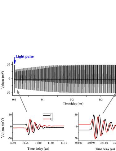
An example for the time-resolved microwave cavity transient method is depicted in Fig. 4. The Q-switch laser pulse (1 ms repetition rate) triggers a train of pulses (each with a duration of 0.5 s followed by another 1.5 s waiting time) which drives the microwave PIN diode. The microwave cavity responds with switch-on and off transients. We measure the microwave transients immediately after switching off the microwave excitation as therein the exciting microwave signal is absent. Thus the transient contains information about the resonator only, free from any further signals and can thus be considered as a null measurement of the relevant information.
Two examples for such IQ traces are shown in Fig. 4 for different time delays after the light pulse. These signals are then Fourier transformed to which Lorentzian curves can be fitted. The fitting yields the eigenfrequency and bandwidth of the cavity as a function of the time delay. These directly give the microwave resonator shift and loss, which allows determination of the material parameters according to Eq. Landau and Lifschitz, 1984.
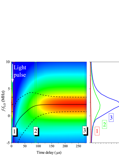
This type of measurement can be also conveniently shown in a three-dimensional contour plot. In Fig. 5., we show the result of the time-resolved resonator readout method for a single crystal silicon wafer sample () with a relatively long (about 100 s) charge carrier recombination time. The contour plot also shows the time-dependent (solid curve) and the half maximum value points of the Lorentzian (dashed curves). The vertical separation between the latter two curves is the resonator bandwidth, BW, which gives . A clear time dependence of both and is observable from the data. The right hand side of Fig. 5. shows individual Lorentzian resonance profiles which are shown for three different time delays.
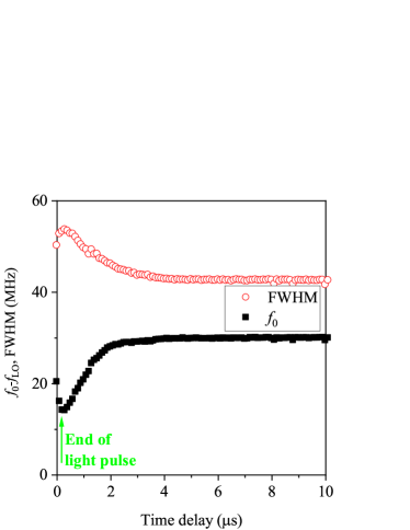
Fig. 6 shows a time-resolved resonator detected -PCD traces for a Si wafer sample which showed an ultrafast charge carrier dynamics less than 2 s. This was performed on a sample with an already low resistivity, , which reduced the cavity quality factor to about . This results in a short cavity transient time of about . This allowed to perform the cavity transient experiment with a repetition time of 200 ns (time resolution is about the symbol size in the figure), which contained a switch on duration of 50 ns. Clearly, the time-dependent variation of both and the BW () can be observed from the data. This shows that our method works well for charge carrier life-times down to the microsecond range.
Finally, we highlight several key points of the present development: our approach does not require frequency stabilization, or AFC, which was required in alternative studies Subramanian et al. (1998); Fessenden et al. (1982), except that the irradiating microwave pulse should be within about 10-100 times the resonator BW with respect to the resonance frequency. Another important aspect is that we obtain the resonator parameters, and , directly from the data, without the need for an involved modeling of the microwave cavity transmission or reflection. Nevertheless, obtaining the time-dependent material parameters ( and ) also requires a calculation according to Eq. (4).
The utility of the present method in an industrial environment remains to be addressed. We believe that it may find better applications in the research of novel semiconductors such as e.g. novel photovoltaic perovskites Chouhan et al. (2017); Labram and Chabinyc (2017); Guse et al. (2016); Bi et al. (2016) and low dimensional semiconductor materials including carbon nanotubes Freitag et al. (2003); Lu and Panchapakesan (2006), graphene Vasko and Ryzhii (2008); Docherty et al. (2012), transition metal dichalcogenides Xia et al. (2014), and black phosphorus Liu et al. (2016); Miao et al. (2017). For such materials sensitivity to material parameters, as well as a sensitive (i.e. background reflection free) measurement of the -PCD signal are important rather than the large throughput study of an industrial investigation.
IV Summary
In summary, we presented an improved approach to detect photoinduced conductivity in semiconductors using microwave resonators. Previous studies with microwave resonators have yielded material parameters after involved modeling or with a slow time dynamics (beyond a few ms-second). Our approach yields directly the resonator parameters, which are in turn related to the material parameters. It is based on the detection of the transient response of a microwave cavity. While the method encompasses all the known benefits of resonators in terms of sensitivity and accuracy, its ultimate time resolution is the resonator time constant which can be as low as a few ns.
Acknowledgements
The Authors are indebted to Dr. Dario Quintavalle from the Semilab Semiconductor Physics Laboratory Ltd. for useful advises and for providing manufacturing grade silicon wafer samples. This work was supported by the Hungarian National Research, Development and Innovation Office (NKFIH) Grant Nrs. 2017-1.2.1-NKP-2017-00001 and K119442, and by the BME-Nanonotechnology FIKP grant of EMMI (BME FIKP-NAT).
References
- Ohsawa et al. (1983) A. Ohsawa, K. Honda, R. Takizawa, and N. Toyokura, Review of Scientific Instruments 54, 210 (1983).
- Kunst and Beck (1986) M. Kunst and G. Beck, Journal of Applied Physics 60, 3558 (1986).
- Lauer et al. (2008) K. Lauer, A. Laades, H. Ubensee, H. Metzner, and A. Lawerenz, Journal of Applied Physics 104, 104503 (2008).
- Berger et al. (2011) B. Berger, N. Schüler, S. Anger, B. Gründig-Wendrock, J. R. Niklas, and K. Dornich, physica status solidi (a) 208, 769 (2011).
- Chouhan et al. (2017) A. S. Chouhan, N. P. Jasti, S. Hadke, S. Raghavan, and S. Avasthi, Current Applied Physics 17, 1335 (2017).
- Labram and Chabinyc (2017) J. G. Labram and M. L. Chabinyc, Journal of Applied Physics 122, 065501 (2017).
- Guse et al. (2016) J. A. Guse, A. M. Soufiani, L. Jiang, J. Kim, Y.-B. Cheng, T. W. Schmidt, A. Ho-Baillie, and D. R. McCamey, Phys. Chem. Chem. Phys. 18, 12043 (2016).
- Bi et al. (2016) Y. Bi, E. M. Hutter, Y. Fang, Q. Dong, J. Huang, and T. J. Savenije, The Journal of Physical Chemistry Letters 7, 923 (2016).
- Novikov et al. (2010) G. Novikov, A. A. Marinin, and E. V. Rabenok, Instruments and Experimental Techniques 53, 233 (2010).
- Freitag et al. (2003) M. Freitag, Y. Martin, J. A. Misewich, R. Martel, and P. Avouris, Nano Lett. 3, 1067 (2003).
- Lu and Panchapakesan (2006) S. Lu and B. Panchapakesan, Nanotechnology 17, 1843 (2006).
- Vasko and Ryzhii (2008) F. T. Vasko and V. Ryzhii, Phys. Rev. B 77, 195433 (2008).
- Docherty et al. (2012) C. J. Docherty, C.-T. Lin, H. J. Joyce, R. J. Nicholas, L. M. Herz, L.-J. Li, and M. B. Johnston, Nature Communications 3, 1228 (2012).
- Xia et al. (2014) F. Xia, H. Wang, D. Xiao, M. Dubey, and A. Ramasubramaniam, Nature Photonics 8, 899 (2014).
- Liu et al. (2016) F. Liu, C. Zhu, L. You, S.-J. Liang, S. Zheng, J. Zhou, Q. Fu, Y. He, Q. Zeng, H. J. Fan, et al., Advanced Materials 28, 7768 (2016).
- Miao et al. (2017) J. Miao, B. Song, Q. Li, L. Cai, S. Zhang, W. Hu, L. Dong, and C. Wang, ACS Nano 11, 6048 (2017).
- Infelta et al. (1977) P. P. Infelta, M. P. de Haas, and J. M. Warman, Radiation Physics and Chemistry (1977) 10, 353 (1977), ISSN 0146-5724.
- Fessenden et al. (1982) R. W. Fessenden, P. M. Carton, H. Shimamori, and J. C. Scaiano, The Journal of Physical Chemistry 86, 3803 (1982).
- Reid et al. (2017) O. G. Reid, D. T. Moore, Z. Li, D. Zhao, Y. Yan, K. Zhu, and G. Rumbles, Journal of Physics D: Applied Physics 50, 493002 (2017).
- Pozar (2004) D. M. Pozar, Microwave Engineering (John Wiley & Sons, Inc., 2004).
- Cetinoneri et al. (2010) B. Cetinoneri, Y. A. Atesal, R. A. Kroeger, G. Tepper, J. Losee, C. Hicks, M. Rasmussen, and G. M. Rebeiz, in 2010 IEEE MTT-S International Microwave Symposium (2010), pp. 469–472, ISSN 0149-645X.
- Subramanian et al. (1998) V. Subramanian, V. R. K. Murthy, and J. Sobhanadri, Journal of Applied Physics 83, 837 (1998).
- Amato (1982) J. Amato, Review of Scientific Instruments 53, 776 (1982).
- Eckstrom et al. (1987) D. J. Eckstrom, M. S. Williams, and J. Dickinson, Review of Scientific Instruments 58, 2244 (1987).
- Kessick et al. (2000) R. Kessick, G. Tepper, E. Lee, and R. James, Journal of Applied Physics 87, 2408 (2000).
- Tepper and Losee (2001) G. Tepper and J. Losee, Nuclear Instruments and Methods in Physics Research Section A: Accelerators, Spectrometers, Detectors and Associated Equipment 458, 472 (2001), ISSN 0168-9002, proc. 11th Inbt. Workshop on Room Temperature Semiconductor X- and Gamma-Ray Detectors and Associated Electronics.
- Braggio et al. (2014) C. Braggio, G. Carugno, A. Lombardi, G. Ruoso, and R. Sirugudu, Journal of Applied Physics 116, 044513 (2014).
- Petersan and Anlage (1998) P. J. Petersan and S. M. Anlage, Journal of Applied Physics 84, 3392 (1998).
- Luiten (2005) A. Luiten, Q-Factor Measurements (John Wiley & Sons, Inc., 2005), Encyclopedia of RF and Microwave Engineering.
- Kajfez (2005) D. Kajfez, Q-Factor (John Wiley & Sons, Inc., 2005), Encyclopedia of RF and Microwave Engineering.
- Gyüre et al. (2015) B. Gyüre, B. G. Márkus, B. Bernáth, F. Murányi, and F. Simon, Review of Scientific Instruments 86, 094702 (2015).
- Gyüre-Garami et al. (2018) B. Gyüre-Garami, O. Sági, B. G. Márkus, and F. Simon, Review of Scientific Instruments 89, 113903 (2018).
- Ernst (1992) R. R. Ernst, Angewandte Chemie-International Edition in English 31, 805 (1992).
- Hodges et al. (2004) J. Hodges, H. Layer, W. Miller, and G. Scace, Review of Scientific Instruments 75, 849 (2004).
- Hodges and Ciurylo (2005) J. Hodges and R. Ciurylo, Review of Scientific Instruments 76, 023112 (2005).
- Cygan et al. (2011) A. Cygan, D. Lisak, P. Maslowski, K. Bielska, S. Wojtewicz, J. Domyslawska, R. S. Trawinski, R. Ciurylo, H. Abe, and J. T. Hodges, Review of Scientific Instruments 82, 063107 (2011).
- Truong et al. (2013) G. W. Truong, D. A. Long, A. Cygan, D. Lisak, R. D. van Zee, and J. T. Hodges, J. Chem. Phys. 138, 094201 (2013).
- Schmitt and Zimmer (1966) H. J. Schmitt and H. Zimmer, IEEE Transactions on Microwave Theory and Techniques MT14, 206 (1966).
- Gallagher (1979) W. Gallagher, IEEE Transactions on Nuclear Science 26, 4277 (1979).
- Komachi and Tanaka (1974) Y. Komachi and S. Tanaka, Journal of Physics E: Scientific Instruments 7, 905 (1974).
- Quine et al. (2011) R. W. Quine, D. G. Mitchell, and G. R. Eaton, Concepts in Magnetic Resonance Part B: Magnetic Resonance Engineering 39B, 43 (2011).
- Connes and Connes (1966) J. Connes and P. Connes, J. Opt. Soc. Am. 56 (1966).
- Fellgett (1949) P. B. Fellgett, Theory of Infra-Red Sensitivities and its Application to Investigations of Stellar Radiation in the Near Infra-Red (PhD thesis). (University of Cambridge, 1949).
- G. Márkus et al. (2018) B. G. Márkus, B. Gyüre-Garami, O. Sági, G. Csősz, A. Karsa, F. Márkus, and F. Simon, physica status solidi (b) 255 (2018).
- Gresits et al. (2019) I. Gresits, G. Thuróczy, O. Sági, I. Homolya, G. Bagaméry, D. Gajári, M. Babos, P. Major, B. G. Márkus, and F. Simon, Journal of Physics D: Applied Physics 52, 375401 (2019).
- Chen et al. (2004) L. Chen, C. Ong, C. Neo, V. Varadan, and V. Varadan, Microwave Electronics: Measurement and Materials Characterization (John Wiley & Sons, Inc., 2004).
- Ristic et al. (2004) S. Ristic, A. Prijic, and Z. Prijic, Serbian Journal of Electrical Engineering 1, 237 (2004).
- Buravov and Shchegolev (1971) L. I. Buravov and I. F. Shchegolev, Instrum. Exp. Tech. 14, 528 (1971).
- Klein et al. (1993) O. Klein, S. Donovan, M. Dressel, and G. Grüner, International Journal of Infrared and Millimeter Waves 14, 2423 (1993).
- Landau and Lifschitz (1984) L. D. Landau and E. M. Lifschitz, Electrodynamics of Continuous Media, Course of Theoretical Physics, Vol. 8 (Pergamon Press, Oxford, UK, 1984).
- Donovan et al. (1993) S. Donovan, O. Klein, M. Dressel, K. Holczer, and G. Grüner, International Journal of Infrared and Millimeter Waves 14, 2459 (1993).
- Dressel et al. (1993) M. Dressel, O. Klein, S. Donovan, and G. Grüner, International Journal of Infrared and Millimeter Waves 14, 2489 (1993).
- Klein et al. (1994) O. Klein, E. J. Nicol, K. Holczer, and G. Grüner, Phys. Rev. B 50, 6307 (1994).
- Thurber et al. (1980a) W. R. Thurber, R. L. Mattis, Y. M. Liu, and J. J. Filliben, Journal of The Electrochemical Society 127, 2291 (1980a).
- Thurber et al. (1980b) W. R. Thurber, R. L. Mattis, Y. M. Liu, and J. J. Filliben, Journal of The Electrochemical Society 127, 1807 (1980b).
- Poole (1996) C. P. Poole, Electron Spin Resonance: A Comprehensive Treatise on Experimental Techniques, Dover Books on Physics (Dover Publications, 1996), ISBN 9780486694443.
Appendix A Physical background of the -PCD measurement
In this section, we summarize the most important background knowledge and some supplementary data to the main text.
In Fig. 7. we show the -PCD results for a silicon single crystal sample which was detected with the conventional method: a silicon wafer covered entirely a WR90 waveguide. The reflected microwaves were detected from it with and without light illumination. In order to calibrate the vertical scale of the -PCD traces, it is desired to calibrate the reflected microwave signal voltage by samples with known resistivity. This would enable to obtain the amount of additional charge carriers from the microwave signal. In the following, we denote the reflected signal by without illumination, and the additional light-induced signal by . We denote the corresponding reflection amplitudes, the parameter, as ”dark” and ”illuminated”.
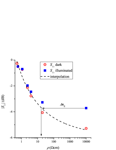
Dashed curve is a purely phenomenological interpolation function (i.e. without any theoretical background) which enables to read out the versus correspondence. We used . Clearly, when illuminated, there is an extra reflection due to the metallicity of the sample. The extra reflection can be connected to a modified sample resistivity as arrows depict in the figure. This ”illuminated-resisvitity” can be used to determine the amount of light-induced excess charge carrier content from the well-known doping versus resistivity plots Thurber et al. (1980a, b).
This enabled us to determine the excess charge carrier concentration for each measurement as a function of time. The latter information is available from the -PCD traces which contain the time-dependent .
To complete the analysis, we require the charge carrier recombination time, , from the -PCD traces, also as a function of time. It is known for the light-induced excess charge carriers that the recombination rate depends on the excess charge carrier concentration itselfLauer et al. (2008). This leads to a time dependence of itself. This can be modelled as .
We obtain:
| (7) |
In practice, the constant subtraction can be performed, which yields the time-dependent .
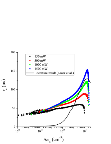
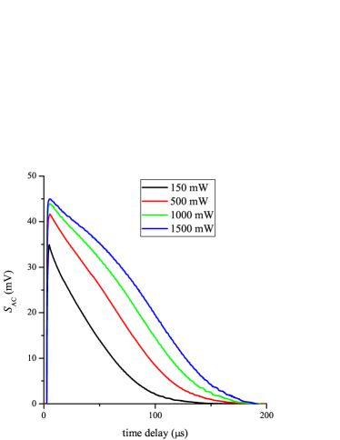
Fig. 9. shows the result of our analysis: namely versus is shown for various exciting laser powers. Ideally, all curves with different powers should fall on one another which is not the case in our data. We speculate that this is due to either heating of the sample or due to charge carrier diffusion. The latter effect influences the microwave reflectivity as the charge carrier concentration is inhomogeneous along the depth profile of the wafer Lauer et al. (2008). Nevertheless, the trends for all curves agree well with the literature data from Ref. Lauer et al., 2008, especially around the longest .
The excess charge carrier lifetime is limited by various relaxation rate contributions as follows:
| (8) |
where , , are the radiative, Auger, Shockley–Read–Hall lifetime contributions, respectively. The radiative lifetime, i.e. electron-hole radiative recombination is significant at high electron-hole concentrations. Similarly, the Auger process (the electron-hole recombination energy is taken away by a free charge carrier) becomes significant for high excess charge carrier concentrations. The Shockley–Read–Hall process occurs due to impurities which form mid-gap states, e.g. Fe and Cr are known to be typical contaminant is silicon. The SRH process probability decreases on higher charge carrier concentrations but importantly it dominates at low excess charge carrier concentration. Thus measurement of for low provides a direct monitoring mean of the impurity content, which is employed in industrial silicon wafer characterization.
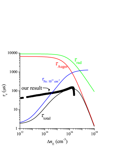
Fig. 10. shows the contributions from the different excess charge recombination mechanisms and also the resulting total for a given Fe impurity content. We also show our data taken at 1500 mW. Note that at the lowest excess charge carrier concentration, our value tends to 25 which is 10 times longer than the example shown herein, indicating an Fe impurity content (provided Fe is the dominant impurity) below .
Appendix B Relation between the generic resonator perturbation and the surface impedance
B.1 The case of a cylinder
Based on Ref. Landau and Lifschitz, 1984, we gave the generic expression for the resonator perturbation for a cylinder with diameter as:
| (9) |
where is a sample size dependent constant (also depends on the cavity mode and electromagnetic field distribution). is the shift in the resonant frequency and is the change in the resonator bandwidth, BW, (or FWHM) given that thus , where we introduced HWHM (half width at half maximum). The authors of Ref. Landau and Lifschitz, 1984 introduced the polarizability:
| (10) |
with being the complex wavenumber of the microwaves inside the material. and are Bessel functions of the first kind.
We then consider the case of finite penetration, i.e. when . Then
| (11) | |||
| (12) |
The relation between the surface impedance and the wave vector is as follows: and (with being the speed of light), which yields: , where is the wavelength of the electromagnetic wave in vacuum.
We have also used the identity:
| (13) |
The in Eq. (12) expresses the fact that the resonator shift is referenced to a perfect conductor (), i.e. one which expels all the electromagnetic fields. This derivation leads us to the well-known formula for the resonator perturbation, which contains the surface impedancePozar (2004); Chen et al. (2004); Klein et al. (1993); Donovan et al. (1993); Dressel et al. (1993):
| (14) |
where is a geometry factor (not dimensionless) that is proportional to the sample surface to the surface of the cavity but it also depends on the resonator mode.
We also note that the shown Re and Im values of can be obtained to match one another when these are shifted by a constant for the case of .
B.2 The case of a sphere
Similarly as before, we can calculate the polarizability of sphere samples from the Helmholtz equation, then we can obtain and from Eq. (9). The polarizability of a sphere sample with diameter is:
| (15) |
where the complex wavenumber is the same as before.
In the case of finite penetration:
| (16) | |||
| (17) |
where we use the identity:
| (18) |
Appendix C The effect of the dielectric constant on the cavity perturbation
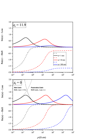
In Fig. 11., we show the effect of a finite for the resonator shift and loss as calculated for a cylinder with varying diameter. Note that in the absence of displacement current related effects (), both the loss and resonator shift terms have the same magnitude. The figure also shows the asymptotic behaviors (doted curves) for the skin limit: Loss , and for the penetration limit: Loss behaviors. When shifted by 2, the shift value matches exactly the loss for the case in the skin-limit.
Appendix D A lumped circuit model calculation of the resonator enhancement effect
We first consider a conventional RLC circuit whose frequency-dependent impedance reads near resonance ():
| (19) |
where the unloaded quality factor reads .

We then consider an RLC circuit whose impedance is matched to the wave impedance of the waveguide, . One can model the matching of microwave resonators by the lumped circuit model in Fig. 12 after Refs. Poole, 1996; Pozar, 2004. The frequency dependent impedance of such a resonator near the resonance, reads:
| (20) |
where is the quality factor of a critically coupled resonator.
The minus sign difference stems from the type of matching element; the sign is + for a capacitive and - for inductive matching (such as that in the figure). Clearly, the difference between Eq. (20) and Eq. (19). is that on resonance its impedance is transformed from the original to . It is less well known that this transformation property is the principal underlying factor why one uses resonators at all, and how the presence of resonators essentially magnify the sensitivity of material properties measurements.
To demonstrate this, we explicitly express the dependence of the matched resonator parameters on the circuit parameters and then we consider a small perturbation to . The perturbation can be thought of as a small extra absorption in the circuit due to the presence of a sample (or eddy current). It can be shown without the loss of generality that similar conclusion can be drawn when the inductivity in the original circuit is perturbed, e.g. by a piece of a magnetic sample such as that using magnetic resonance.
Ref. Pozar, 2004 derives that for the above circuit the resonance and impedance matching conditions are:
| (21) |
where holds.
Clearly, this equation sets the value of . In the high limit, , thus , it thus also shows that the resonance frequency is only slightly shifted with respect to .
We then consider the sensitivity of the circuit return impedance (or ) with respect to . This is obtained from the change in the corresponding impedances as a function of a small perturbation in : . We obtain:
| (22) |
where we used that for an unmatched circuit, such as that described by Eq. (19), the following derivative reads:
| (23) |
The sensitivity of the real part impedance of a matched circuit is on the other hand:
| (24) |
where we used that for the impedance of the matched circuit described by Eq. (12) the derivative reads:
| (25) |
We note that the corresponding first order derivatives for the imaginary parts vanish near resonance for both cases. The striking fact about Eqs. (22) and (24) is that the matched circuit appears to act as an impedance transformer by . We also note that other cases of the resonator perturbation can be similarly considered. E.g. when the resonator is perturbed by a magnetic material, its effect can be taken into account as a change in , as: , where is the (complex) magnetic susceptibility. The acts as if was perturbed by . Thus the above argument applies and the sensitivity for this perturbation reads and its effect is amplified by .
The real part, perturbes by , which has an effect on the imaginary part of . This case:
| (26) |
For the matched case, we obtain:
| (27) |
The enhancement factor is often mistaken by an enhancement effect by (or ), the reason being that for most resonators holds thus . The can be motivated for a waveguide and a corresponding resonator: a fundamental mode rectangular resonator with a mode of TE101, which is made out of a half wavelength section of a TE10 cylindrical waveguide. For both the TE101 cavity and for the TE10 section, the inductivity is , and capacitance is . Given that and , we get exactly . Similar arguments hold for other types of resonators such as e.g. a resonator made of a coplanar waveguide Pozar (2004).
We finally show that one observes a similar up-transformation (i.e. enhancement) effect for the reflection coefficient. Again, we consider the case of the unmatched and matched circuits described by Eqs. (22) and (24), respectively. The reflection coefficients read near resonance (assuming due to the large ):
| (28) |
thus the reflection coefficient is close to 1 for the unmatched case which is often disadvantageous, whereas the matched case represents a null measurement.
The corresponding derivatives read:
| (29) |
Therefore the sensitivity of the reflection coefficient is enhanced by for the case of the matched circuit as compared to the unmatched case.
Appendix E The resonator advantage over a conventional reflection setup
The above discussion is valid for a conventional reflection setup, where the reflected RF voltage is detected with a continuous wave irradiation. As it was shown, the reflectometry method is more sensitive for a matched resonator that for a simple unmatched circuit.
It is also worth discussing the case when the resonator parameters, the frequency shift () and the factor change (), are measured directly. Without the loss of generality, we consider the case of a magnetic sample, whose effect can be well demonstrated. The magnetic sample with a complex susceptibility of perturbs a solenoid of an RF circuit as: , where is the filling factor. Such a sample perturbs the resonator parameters asPoole (1996); Chen et al. (2004):
| (30) |
In the following, we describe the error of the measurement for the non-resonant and resonant cases. In the conventional reflectometry technique, it is obtained from the reflection coefficient, . We consider a waveguide with wave impedance , which is terminated by an inductor with inductance . We then introduce the empty reflection coefficient (i.e. without the sample), , and that with the sample, . This gives:
| (31) |
where we retained leading order terms in only.
We introduce the standard error of the respective measurements as . Error propagation dictates that
| (32) |
the notation is employed as is a complex quantity. Our experience with the conventional reflectometry setup using VNAs shows that the quantity on the right hand side is about , which fixes the attainable accuracy of the susceptibility measurement.
On the other hand, we showed previously Gyüre et al. (2015); Gyüre-Garami et al. (2018) that the standard error of can be expressed as:
| (33) |
where we introduced the resonator bandwidth, BW, which is related to the as . We assumed that is error free as it is a dividing constant. We showed in Refs. Gyüre et al., 2015; Gyüre-Garami et al., 2018 that the quantity is typically . Clearly, a comparison between Eqs. (32) and (33) yields that again, the enhancement in the accuracy of the resonator based measurement is -fold.