Universal light-guiding geometry for high-nonlinear resonators
having molecular-scale roughness
By providing an effective way to leverage nonlinear phenomena in chip-scale, high-Q optical resonators have induced the recent advances of on-chip photonics represented by micro-combsDODOS_Nat and ultra-narrow linewidth lasersJBluementhal_Nat_Si3N4SBS . These achievements mainly relying on Si, SiO2, and Si3N4 are expected to be further improved by introducing new materials having higher nonlinearity. However, establishing fabrication processes to shape a new material into the resonator geometries having extremely smooth surfaces on a chip has been a challenging task. Here we describe a universal method to implement high-Q resonators with any materials which can be deposited in high vacuum. This approach, by which light-guiding cores having surface roughness in molecular-scale is automatically defined along the prepatterned platform structures during the deposition, is verified with As2S3, a typical chalcogenide glass of high-nonlinearity. The Q-factor of the developed resonator is 14.4 million approaching the loss of chalcogenide fibersFiberLoss_NRL , which is measured in newly proposed tunable waveguide-to-resonator coupling scheme with high ideality. Lasing by stimulated Brillouin process is demonstrated with threshold power of 0.53 mW which is 100 times lower than the previous record based on chalcogenide glassesBEggleton_SBSdevice . This approach paves the way for bringing various materials of distinguished virtues to the on-chip domain while keeping the loss performance comparable to that of bulk form.
High-Q optical resonators, which had long been used for scientific researches such as cavity quantum electrodynamicsaoki2006observation and optomechanicskippenberg2008cavity , have become an irreplaceable core of on-chip photonics with huge practical impacts. With dedicated efforts over a past decade, now, resonators can be fabricated on a chip with high Q-factorHLee_Nat_Photonics ; DODOS_Nat ; Lipson_Nat_battery . Their geometry can be precisely designed and shaped to control the major properties such as free spectral range (FSR) and dispersion to satisfy the requirement for the efficient nonlinear processHLee_Nat_Photonics ; KVahala_NatPhoton_DoubleWedge . This advance has implanted versatile functions established in nonlinear optics to on-chip photonics while keeping its own virtues such as miniaturization, mass-productivity, and integration with other active and passive components. Optical frequency comb which revolutionized ultrafast science and metrology is being implemented on a chip based on Kerr nonlinearityDODOS_Nat ; Lipson_Nat_battery . A core part of ultra-narrow linewidth lasersJBluementhal_Nat_Si3N4SBS and highly sensitive optical gyroscopesKVahala_arXiv_gyro have been demonstrated in chip-scale by means of stimulated Brillouin scattering (SBS) process.
There are great motivations to explore various materials although the current achievements are entirely relying on Si, SiO2, Si3N4, the primary materials for integrated photonics. Materials having higher nonlinearity give an opportunity to decrease pump power to the level required for portable devicesBEggleton_Nat_Photonics ; gQ_MLoncar_NatComm_LBO ; gQ_KYvind_Optica_AlGaAS ; JHu_NP_integrated . Materials having extended transmission windows can spread this advance in the near-infrared to neighboring wavelength rangesBEggleton_Nat_Photonics . Accordingly, a lot of attention is paid to develop on-chip high-Q resonators with other promising materials. The most critical part of these attempts is to develop the etch process customized for the particular nature of each material to attain extremely smooth surface since the Q-factor is mainly limited by surface-scattering loss. This challenge which recurs whenever introducing new materials impedes further development of the technology beyond the current state which is limited by the property of the primary materials. To completely address this issue, we propose a universal approach by which high-Q resonators, or more generally light-guiding structures with extremely low loss, can be defined on a chip without the following etch process.
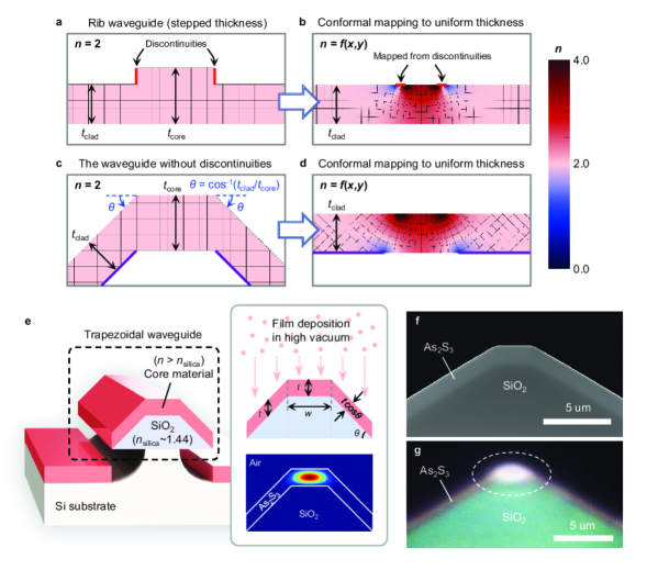
The indispensability of etching or subtractive processes for waveguide fabrications is related to the discontinuity of the waveguide geometry. Transformation optics xu2015conformal provide insight into the origin of the discontinuity. Forming a light-guiding structure can be generally understood as the practical implementation of a core, the domain having a relatively higher refractive index than a surrounding medium. For the most common case of using a single material, a core needs to be defined by controlling the thickness distribution as a rib waveguide shown in Fig. 1a. The refractive index profile of the equivalent flat waveguide in Fig. 1b, which is quasi-conformally transformed from the ribchang2010design , clearly shows higher index around the region corresponding to the thickest part of the original structure. The mapping is performed to result in the equivalent structure having a uniform thickness while keeping the geometry of outer thinner parts, namely a cladding, unchanged. It converts the thickness variation to the index distribution. It is noteworthy that, in conventional approaches, discontinuity or sudden change of the film geometry necessarily occurs around the junction between the thick core and thin cladding as marked by the red lines in Fig. 1a. Therefore, to practically fabricate such discontinuities, it is unavoidable to perform direct etch processes or any indirect processes such as lift-off which cause rough surfaces. Moreover, these rough surfaces strongly interact with the optical modes since they are mapped near the highest index region where most of fields are confined.
To resolve this problem, we introduce a new light-guiding structure without the discontinuities as shown in Fig. 1c. To continuously connect the claddings having a thickness of to the core having a thickness of , the claddings are rotated by which satisfies ). The transformed geometry in Fig. 1d obviously shows the formation of a high index region around the top flat section. This waveguide having continuous junctions can be realized simply by depositing the core material on the bottom platform structure made of SiO2 without subsequent etch processes. As shown in Fig. 1e, the cross-section of the platform structure is a trapezoid having both side slopes corresponding to the characteristic profile formed by wet etchingHLee_Nat_Photonics . The deposition under high vacuum results in the uniform film thickness of along the deposition direction over the whole platform. Therefore, the film thickness on the side slope along the normal direction from the material interface decreases to which satisfies the continuous junction condition for arbitrary values of and .
The design of trapezoidal waveguides involves intrinsic immunity for surface roughness of platform structures. In contrast to the rib waveguide, the etched surfaces of the silica platform marked by the purple lines in Fig. 1c are well separated from the high index region in the transformed geometry. Therefore, optical modes are mainly guided by the surfaces having molecular roughness defined by film deposition and the unetched oxide interface. Moreover, the roughness of the wet-etched silica surface can be suppressed below 1 nm as demonstrated for ultra-high-Q wedge resonatorsHLee_Nat_Photonics .
This universal approach applicable to any materials with a higher refractive index than SiO2 which can be directionally deposited on a wafer is experimentally verified with chalcogenide glass. Chalcogenide glass has attracted great attention due to its distinguished high nonlinearity as well as high transparency in the mid-infrared wavelength rangeBEggleton_Nat_Photonics ; OBang_Nat_Photonics ; FiberLoss_NRL . However, its inherent irregular nature related to the variation of stoichiometry and bond structures tends to cause the characteristic grainy rough surface by nonuniform etch rate in nanoscaleDYChoi_JAP . As a result, the loss performance of on-chip chalcogenide devicesBEggleton_LowlossWG ; JHu_OL_highQ has lagged far behind that of optical fiber formFiberLoss_NRL or theoretical estimationTheoLoss_referedbyNRL despite continuous and dedicated efforts over a decade to tame this particular nature.
The cross-sectional image of the waveguide fabricated with As2S3, a typical chalcogenide glass, is shown in Fig. 1f. It is obvious that the film is uniformly deposited on the SiO2 platform by means of thermal evaporation with a large mean free path (around 500 m at 10-7 torr). The surface roughness of the SiO2 platform and As2S3 film is suppressed below 1 nm, confirmed by atomic force microscopy. The fabrication procedure and details are provided in the method section.
The confinement of the optical mode in the top-flat region is experimentally verified by observing the transmitted mode profile from the cleaved output facet of a straight waveguide with a near-infrared camera as shown in Fig. 1g. This mode profile of 1550 nm wavelength corresponds well to the intensity distribution of the fundamental TE mode simulated by Lumerical Mode Solutions. The coupling loss for end-fire coupling with a lensed fiber is 3.5 dB, attained without serious engineering to match the mode profiles for higher coupling efficiency.
Although on-chip ring resonators can be easily implemented with trapezoidal waveguides, proper coupling scheme is required to efficiently access the modes in the resonators. The efficient coupling for chalcogenide resonators has been a critical issue because of its relatively higher refractive index which cannot be matched by a SiO2 tapered fiber, a well-developed coupling tool in wide useTbirks_OL_taperfiber ; KVahala_PRL_taperfiber . Although there have been considerable efforts to fabricate tapered fibers with chalcogenide glasslecaplain2016mid , its mechanical instability and difficulty in tapering process hinder wide-spread of this technique.
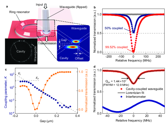
As a general solution to couple with resonators made of any materials, a new flip-chip coupling scheme is developed as shown in Fig. 2a, where an on-chip bus waveguide is flipped over and coupled to a resonator on the other chip. Since both guiding structures have a similar trapezoidal cross-section, the effective refractive indices of their modes match well. The scattered trace of the mode in the coupled chips observed by IR camera which can see structures through the flipped-over chip is shown in the left inset of Fig. 2a. The coupling strength can be adjusted as needed by controlling the gap and offset (Fig. 2a right inset) with a piezo stage. As confirmed in Fig. 2b, the resonance mode in under-coupled and critical-coupled condition clearly fits with Lorentzian function without a vestige of Fano resonance which is typically observed for a multimodal bus waveguide.
For further investigation of the coupling junction performance, the coupling parameter and the ideality have been calculated from the transmission on resonance measured with varying the gap distance between the waveguide and resonatorKVahala_PRL_ideality ; TKippenberg_PRA_ideality . Since the coupling parameter can be adjusted equal to or larger than 1 as shown in Fig. 2c, it is confirmed that over-coupling condition beyond the critical coupling is achievable. The coupling performance is quantified by the ideality of the junction that is the degree to which the junction between a bus waveguide and resonator behave as a true single-mode coupler. As described in detail in the method section, it is confirmed that the ideality value is 0.923 in the critical coupling condition. Here, zero of the ideality means no coupling into the desired mode and unity stands for the perfect single-mode coupler. Therefore, the measured ideality shows that the proposed coupling scheme allows selective and efficient access to the targeted mode without significant power loss or addition of redundant complexity by multimode interaction.
Q-factor, the most important feature, is measured to evaluate the performance of the developed resonators. The dimensions of the resonator are 1.3 m of As2S3 film thickness, 10 m of top width, 30∘ of slope angle, and 4.94 mm of diameter. By scanning the laser frequency, the full width half maximum (FWHM) of the resonance is measured, which is calibrated by the sinusoidal reference signal of 100.63 MHz from a fiber Mach-Zehnder interferometer as shown in Fig. 2d. The maximum Q-factor attained from FWHM of 12.9 MHz is , which is more than 10 times larger than the previous record of the on-chip resonators made of chalcogenide glassJHu_OL_highQ . It should be emphasized that the waveguide loss of 2.77 dB/m converted from the measured Q-factor approaches 0.9 dB/m, the best record of the loss of chalcogenide glass fiber at conventional telecom wavelengthFiberLoss_NRL . This implies that the scattering loss induced by the trapezoidal waveguide is well suppressed to the level of the material loss of chalcogenide glass which is dominated by material absorption and Rayleigh scattering by nanoscale refractive index fluctuation.
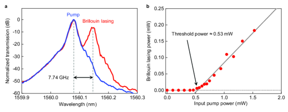
Among the possible applications exploiting the large optical nonlinearity of chalcogenide glass, we demonstrate on-chip lasing based on the SBS process. The dimensions of the resonator are the same as the previous one for Q-measurement, which is designed to place the SBS process in the cavity. FSR of its TE fundamental mode is 7.74 GHz corresponding to the Brillouin phonon frequency in As2S3 at 1560 nm wavelength. Characterization of the Brillouin lasing signal is performed in the measurement setup similar to the previous studiesBEggleton_SBSreview ; KVahala_arXiv_gyro . Figure 3a shows the measured optical spectrum of the back-reflected pump and the Brillouin lasing signal (1st Stokes wave). The beating frequency between them is 7.74 GHz which corresponds to a Brillouin frequency shift of As2S3 fiberssanghera2010nonlinear . In this figure, pump intensity is higher than the Brillouin lasing signal because around 17.5% of the pump is back-reflected at the input facet of the coupled waveguide due to the large difference of refractive index between the air and chalcogenide glass.
Significant reduction of a lasing threshold is achieved by the enhanced Q-factor and Brillouin gain coefficient of As2S3 that is tens of times larger than those of SiO2 and Si3N4. The lasing signal power depending on input pump power is measured while the pump laser is locked to the resonant mode as plotted in Fig. 3b. It shows a typical lasing curve with a slope efficiency of 18%. The lasing threshold is 530 W which is around 100 and 25 times lower than the previous record of the on-chip Brillouin lasers made of chalcogenide and nitride, respectively. It is remarkable that Q-factor is inverse-quadratically related to the threshold power of not only the Brillouin lasing but also the other nonlinear processes such as Raman lasing and four wave mixing.
Additional features proving the potential of this approach are briefly described as follows. It is numerically demonstrated that dispersion can be geometrically controlled by adjusting the structure of the trapezoidal waveguides. Considering the ease of stacking multilayer cores in thickness resolution of nanometer-scale, precise dispersion control through material combination is also achievable. For mid-IR application, excess material absorption caused by SiO2 platform can be completely prevented by depositing a bottom cladding layer before the core deposition.
In summary, we have presented the universal approach to define the light-guiding structure of extremely smooth surfaces on a chip without etching the core materials as well as the flip-chip coupling scheme to evanescently couple the developed resonators with the high coupling ideality. By applying this scheme to chalcogenide glass, the threshold of the on-chip Brillouin laser is reduced by about 100 times than that of the previous chalcogenide devices, by means of the enhanced Q-factor which is close to the loss of state-of-the-art optical fibers made of the same material. This universal method can be applied to bring the other materials having distinguished merits to the on-chip domain while keeping the loss performance comparable to that of bulk form.
Acknowledgments This work was supported by Samsung Research Funding & Incubation Center of Samsung Electronics under Project Number SRFC-IT1801-03.
Author Contributions All authors made important contributions to the work.
Competing interests The authors declare no competing financial interests.
Correspondence and requests for materials should be addressed to D.-Y.C. and H.L.
METHODS
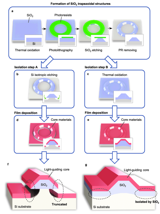
Formation of SiO2 trapezoidal platform. Extended Data Fig. 1a shows details for forming SiO2 trapezoidal platform. First, a layer of SiO2 is thermally grown with a thickness of 8 m on a prime-grade (100) Si wafer in a furnace system (Tytan Mini 1800, TYSTAR). The SiO2 layer is treated with hexamethyldisilazane (HMDS) vapor prime process to modify surface adhesion property. To define the SiO2 trapezoidal platform, we then pattern photoresists on the SiO2 layer with a mask aligner lithography system (MA6 Mask Aligner, Karl Suss). The patterned photoresist is used as an etch mask for the following wet-etching process. The wet etching of SiO2 layer is done with buffered hydrofluoric acid (BHF) solution. The slope angle of the platform can be controlled in the range from 5∘ to 60∘ according to the adhesion property between the photoresist and the SiO2 layer, which is mainly controlled with the HMDS treatment step. In addition, by repeating the steps through the photolithography and wet-etching, the slope angle can reach larger values than the normal range attained by a single processKVahala_NatPhoton_DoubleWedge . The details for realizing the smooth etched surface with desired slope angle is described in the previous workHLee_Nat_Photonics . After the wet-etching, a cleaning process with organic solvents is performed to remove the photoresist.
Isolation from Si substrate. Once the SiO2 trapezoidal platform is formed, we isotropically etch the Si substrate under the platform with XeF2 gas (XeF2 etching system, Teraleader Co. Ltd.) as shown in Extended Data Fig. 1b. By having this step, the optical field at the trapezoidal waveguide is perfectly isolated from the Si substrate to prevent leakage to the substrate. Alternatively, the optical field can be isolated from the substrate by growing a thermal oxide film on the Si substrate exposed by the wet-etching (Extended Data Fig. 1c).
Film deposition. Once the isolation step is done, a material deposition step follows (Extended Data Fig. 1 f,g). The material we use for the light-guiding core in this paper is As2S3 (AMTIR-6, Amorphous Materials Inc.), and the thickness is 1.3 m. The material is deposited with thermal evaporation process, and the deposition direction is normal to the wafer substrate. After the deposition, 2 nm-thick Al2O3 layer is formed on the surface by atomic layer deposition for surface passivation. A two-step annealing process (thermal and light annealing) reported in the previous work is performed to bring the As2S3 film close to the bulk stateDChoi_PP_ChGannealing . To estimate surface roughness of the waveguide, we analyzed a topography of the waveguide surfaces using atomic force microscopy (AFM). On the bare SiO2 structure, the roughness on the top and the wedge was 0.3 and 0.8 nm, respectively. Whereas on the as-deposited As2S3 surface, the roughness on the top and the wedge was 0.3 and 0.6 nm, respectively.
Calculating coupling ideality, . Details for calculating coupling parameters and ideality can be found in the previous studiesKVahala_PRL_ideality ; TKippenberg_PRA_ideality , but are summarized here for the convenience of the reader. Coupling parameter can be calculated from transmission of the waveguide (coupled to the resonator at resonant wavelength) using the following equation (upper signs for the over-coupled regime and lower signs for the under-coupled regime). can be decomposed into an intrinsic contribution and a parasitic contribution , which stand for the coupling of a resonator mode to a fundamental mode and the other various parasitic components including higher order modes, respectively, so that 1/ = 1/+1/. and can be found by asymptotically fitting gap versus graph (in logarithmic scale) with two lines (Fig. 2c). The line with smaller slope indicates and the line with larger slope indicates . Coupling ideality, , can be calculated from by using the following equation I = 1/(1+). The parasitic coupling parameter which is clearly revealed in the gap less than -0.1 m in the figure gives the ideality value of 0.923 in the critical coupling condition.
Data availability. The data sets generated and/or analysed during the current study are available from the corresponding authors on reasonable request.
References
- (1) Spencer, D. T. et al. An optical-frequency synthesizer using integrated photonics. Nature 557, 81 (2018).
- (2) Gundavarapu, S. et al. Sub-hertz fundamental linewidth photonic integrated Brillouin laser. Nature Photonics 13, 60–67 (2019).
- (3) Kim, W. et al. Recent progress in chalcogenide fiber technology at NRL. Journal of Non-Crystalline Solids 431, 8–15 (2016).
- (4) Morrison, B. et al. Compact Brillouin devices through hybrid integration on silicon. Optica 4, 847–854 (2017).
- (5) Aoki, T. et al. Observation of strong coupling between one atom and a monolithic microresonator. Nature 443, 671 (2006).
- (6) Kippenberg, T. J. & Vahala, K. J. Cavity optomechanics: back-action at the mesoscale. science 321, 1172–1176 (2008).
- (7) Lee, H. et al. Chemically etched ultrahigh-Q wedge-resonator on a silicon chip. Nature Photonics 6, 369–373 (2012).
- (8) Stern, B., Ji, X., Okawachi, Y., Gaeta, A. L. & Lipson, M. Battery-operated integrated frequency comb generator. Nature 562, 401 (2018).
- (9) Yang, K. Y. et al. Broadband dispersion-engineered microresonator on a chip. Nature Photonics 10, 316–320 (2016).
- (10) Lai, Y.-H., Lu, Y.-K., Suh, M.-G. & Vahala, K. Enhanced sensitivity operation of an optical gyroscope near an exceptional point. arXiv preprint arXiv:1901.08217 (2019).
- (11) Eggleton, B. J., Luther-Davies, B. & Richardson, K. Chalcogenide photonics. Nature Photonics 5, 141–148 (2011).
- (12) Wang, C. et al. Monolithic lithium niobate photonic circuits for Kerr frequency comb generation and modulation. Nature Communications 10, 978 (2019).
- (13) Pu, M., Ottaviano, L., Semenova, E. & Yvind, K. Efficient frequency comb generation in AlGaAs-on-insulator. Optica 3, 823–826 (2016).
- (14) Li, L. et al. Integrated flexible chalcogenide glass photonic devices. Nature Photonics 8, 643–649 (2014).
- (15) Xu, L. & Chen, H. Conformal transformation optics. Nature Photonics 9, 15 (2015).
- (16) Chang, Z., Zhou, X., Hu, J. & Hu, G. Design method for quasi-isotropic transformation materials based on inverse Laplace’s equation with sliding boundaries. Optics express 18, 6089–6096 (2010).
- (17) Petersen, C. R. et al. Mid-infrared supercontinuum covering the 1.4-13.3 m molecular fingerprint region using ultra-high NA chalcogenide step-index fibre. Nature Photonics 8, 830–834 (2014).
- (18) Choi, D.-Y., Madden, S., Rode, A., Wang, R. & Luther-Davies, B. Nanoscale phase separation in ultrafast pulsed laser deposited arsenic trisulfide (As2S3) films and its effect on plasma etching. Journal of Applied Physics 102, 083532 (2007).
- (19) Madden, S. J. et al. Long, low loss etched As2S3 chalcogenide waveguides for all-optical signal regeneration. Optics Express 15, 14414–14421 (2007).
- (20) Du, Q. et al. Low-loss photonic device in Ge–Sb–S chalcogenide glass. Optics Letters 41, 3090–3093 (2016).
- (21) Dianov, E. M., Petrov, M. Y., Plotnichenko, V. G. & Sysoev, V. K. Estimate of the minimum optical losses in chalcogenide glasses. Soviet Journal of Quantum Electronics 12, 498 (1982).
- (22) Knight, J. C., G. Cheung, F. J. & Birks, T. A. Phase-matched excitation of whispering-gallery-mode resonances by a fiber taper. Optics Letters 22, 1129–1131 (1997).
- (23) Cai, M., Painter, O. & Vahala, K. J. Observation of critical coupling in a fiber taper to a silica-microsphere whispering-gallery mode system. Physics Review Letters 85, 74–77 (2000).
- (24) Lecaplain, C., Javerzac-Galy, C., Gorodetsky, M. & Kippenberg, T. Mid-infrared ultra-high-Q resonators based on fluoride crystalline materials. Nature communications 7, 13383 (2016).
- (25) Spillane, S. M., Kippenberg, T. J., Painter, O. J. & Vahala, K. J. Ideality in a fiber-taper-coupled microresonator system for application to cavity quantum electrodynamics. Physics Review Letters 91, 043902 (2003).
- (26) Pfeiffer, M. H. P., Liu, J., Geiselmann, M. & Kippenberg, T. J. Coupling ideality of integrated planar high-Q microresonators. Physical Review Applied 7, 024026 (2017).
- (27) Eggleton, B. J., Poulton, C. G. & Pant, R. Inducing and harnessing stimulated Brillouin scattering in photonic integrated circuits. Advances in Optics and Photonics 5, 536–587 (2013).
- (28) Sanghera, J. S. et al. Nonlinear properties of chalcogenide glass fibers. International Journal of Applied Glass Science 1, 296–308 (2010).
- (29) Choi, D.-Y. et al. Photo-induced and thermal annealing of chalcogenide films for waveguide fabrication. Physics Procedia 48, 196–205 (2013).