Large piezoelectric coefficients combined with high electron mobilities in Janus monolayer XTeI (X=Sb and Bi): a first-principle study
Abstract
The absence of both the inversion symmetry and out-of-plane mirror symmetry together with spin-orbit coupling (SOC) can induce novel electronic and piezoelectric properties. In this work, the piezoelectric properties along with carrier mobilities of Janus monolayer XTeI (X=Sb and Bi) are studied by density functional theory (DFT). By using generalized gradient approximation (GGA) plus SOC, they are found to be indirect gap semiconductors with the Rashba spin splitting. The piezoelectric tensors of Janus monolayer XTeI (X=Sb and Bi) are reported by using density functional perturbation theory (DFPT). Due to lacking both the inversion symmetry and out-of-plane mirror symmetry for Janus monolayer XTeI (X=Sb and Bi), both in-plane and out-of-plane piezoelectric effects can be observed, and the large piezoelectric coefficients are predicted (e.g. =12.95 pm/V for SbTeI and =8.20 pm/V for BiTeI), which are comparable and even higher than ones of many other two-dimensional (2D) materials and other well-known bulk piezoelectric materials, especially for out-of-plane piezoelectric coefficients. With GGA+SOC, the high electron carrier mobilities are obtained, and the electron mobility of BiTeI along armchair direction reaches up to about 1319 . The carrier mobility shows a rather pronounced anisotropy between electron and hole/armchair and zigzag directions. It is found that tensile strain can improve the piezoelectric coefficients of Janus monolayer XTeI (X=Sb and Bi). For example, at 4% strain, the of SbTeI (BiTeI) is up to 20.12 pm/V (11.48 pm/V), compared with unstrained 12.95 pm/V (8.20 pm/V). Our works imply Janus monolayer XTeI (X=Sb and Bi) have potential applications in flexible electronics and piezoelectric devices, and can stimulate further experimental works.
pacs:
71.20.-b, 77.65.-j, 72.15.Jf, 78.67.-n Email:sandongyuwang@163.comI Introduction
Compared to their bulk counterparts, 2D materials can show some unique or surprising properties, like high mechanical strengthq1 , high photocatalytic activityq2 , remarkable optical and magnetic propertiesq3 . Due to potential nanoscale piezoelectric applications, the piezoelectricity in 2D materias has attracted growing interestq4 , which can be used in sensors, actuators and energy sources. A piezoelectric material must be non-centrosymmetric, and should have a band gap for prohibiting current leakage. For 2D materials, the reduction in dimensionality leads to that their inversion symmetry is often eliminated, allowing them to become piezoelectric. Due to the inversion asymmetry in the 2H phase, the monolayer as a typical example have been proved to possess piezoelectricity experimentally (=2.9 C/m)q5 ; q6 . A large in-plane piezoelectricity and additional out-of-plane piezoelectricity have been predicted in 2D Janus transition metal dichalchogenides (TMD)q7 , which can directly break the inversion symmetry and out-of-plane mirror symmetry. Recently, the existence of vertical dipoles has been experimentally proved in the Janus MoSSe monolayer, which shows an intrinsic vertical piezoelectric responseq8 . In theory, the piezoelectric properties of lots of 2D materials have been reportedq7 ; q9 ; q10 ; q11 ; q12 , like metal dichalcogenides, group IIA and IIB metal oxides, group III-V semiconductors and Janus TMD.

Janus monolayer SbTeI and BiTeI have been predicted theoretically with a low formation energy, and they are dynamically stableq13 ; q14 . The bulk SbTeI or BiTeI has a layered structure along its crystallographic c axis, and a Bi or Sb atom is sandwiched between one Te and one I, forming a triple layer. Within each triple layer, these atoms have strong chemical bonding, but the adjacent triple layers are weakly coupled via the van der Waals interactions. Thus, Janus monolayer SbTeI and BiTeI can be exfoliated from their bulks. The Rashba spin splitting in monolayer SbTeI or BiTeI has been reported with a sizable Rashba coupling parameter of 1.39 eV or 1.97 eVq14 , and they are potentially useful for spintronics, like spin-polarized field effect transistor. Recently, we have predicted that Janus monolayer SbTeI and BiTeI may be potential 2D thermoelectric materials due to very low lattice thermal conductivitiesq15 . However, to the best of our knowledge, no studies have been reported on piezoelectric properties of Janus monolayer SbTeI and BiTeI. In this work, inspiring from their special Janus structure of monolayer SbTeI or BiTeI, their piezoelectric properties along with carrier mobilities are studied by density functional theory (DFT). Calculated results show they have the large piezoelectric coefficients (e.g. =12.95 pm/V for SbTeI and =8.20 pm/V for BiTeI), which are comparable and even higher than ones of many other 2D materialsq7 ; q9 ; q11 ; q12 and other well-known bulk piezoelectric materialsaln ; aln-1 ; aln-2 ; aln-3 ; aln-4 , especially for out-of-plane piezoelectric coefficients with respect to other ones of 2D materials. The high electron carrier mobilities are also predicted, for example about 1319 for the electron mobility of BiTeI along armchair direction. It is proved that the tensile strain can make the of SbTeI (BiTeI) to be up to 20.12 pm/V (11.48 pm/V) from unstrained 12.95 pm/V (8.20 pm/V), increased by 55% (40%). These results make us believe that Janus monolayer SbTeI and BiTeI may be potential 2D piezoelectric materials, and can stimulate further experimental synthesis of these monolayers.
| 4.32 (4.42) | 28.52 (26.91) | 7.72 (7.93) | 10.4 (9.49) |
| 26.43 (24.57) | 0.271 (0.295) | 0.89 (0.67) | 17.2 (40.1) |
II Computational detail
Based on DFT1 , our calculations are performed using the projected augmented wave (PAW) method with a kinetic cutoff energy of 500 eV, as implemented in the VASP packagepv1 ; pv2 ; pv3 . The popular GGA of Perdew, Burke and Ernzerhof (GGA-PBE)pbe is used as the exchange-correlation potential, and the SOC was included self-consistently. For the Janus monolayer SbTeI and BiTeI, a vacuum spacing of more than 18 along the z direction is included to avoid interactions between two neighboring images. The total energy convergence criterion is set to eV. The geometry optimization was considered to be converged with the residual force on each atom being less than 0.001 . To obtain the piezoelectric properties of the Janus monolayer SbTeI and BiTeI, the elastic stiffness tensor are calculated by using the finite difference method (FDM), and the piezoelectric stress coefficients are calculated by DFPT methodpv6 by the VASP package. Both elastic and piezoelectric stress coefficients, including both the ionic and electronic components, have been calculated. Within FDM and DFPT, the the electronic and ionic contribution to the elastic and piezoelectric stress coefficient can be given directly from VASP code. The 2D elastic coefficients and piezoelectric stress coefficients have been renormalized by the the length of unit cell along z direction (): = and =.
III Electronic structures
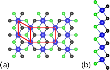
The geometric structure of the Janus XTeI (X=Sb and Bi) is plotted in Figure 1, which consists of of three atomic layers with X sandwiched between the Te and I layers. The structure is similar to Janus TMD monolayer PtSSeq7-0 and SnSSeq7-2 . Both rhombus primitive cell and rectangle supercell are shown, and calculating carrier mobilities and piezoelectric coefficients need to use rectangle supercell. The armchair and zigzag directions of the rectangular supercell are defined as x and y directions, respectively. Their symmetry is , which lacks the reflection symmetry with respect to the central X atoms. The lattice constant of the Janus monolayer SbTeI and BiTeI are 4.32 and 4.42 , which agree well previous theoretical valuesq14 ; q15 . It have been proved that the SOC has very important effects on their electronic structuresq13 ; q14 ; q15 , thus only GGA+SOC energy bands of monolayer SbTeI and BiTeI are plotted in Figure 2. Around the Fermi level, all the bands are dominated by the p-orbits with conduction band minimum (CBM) being Sb/Bi-p and valence band maximum (VBM) being Te-pq13 . The Janus monolayer SbTeI (BiTeI) is found to be a semiconductors with an indirect band gap of 0.89 eV (0.67 eV) with GGA+SOC. The CBM is located at slightly away from the point along the -K or -M paths, and the VBM is between the and K or M points. The Rashba-like and Zeeman-like band splitting can be observed, which is due to the absence of vertical mirror symmetry combined with the SOC effect. The Rashba spin splitting in the lowest conduction band at the high-symmetric point can be clearly seen, and their Rashba energy, defined as the band crossing point of the conduction bands at the point minus the energy of the CBM, are 17.2 meV and 40.1 meV, respectively, which are consistent with the previously reported valuesq13 ; q14 ; q15 .
| Name | ||||
|---|---|---|---|---|
| SbTeI | 2.69 | 12.95 | -0.13 | -0.37 |
| BiTeI | 1.56 | 8.20 | -0.23 | -0.66 |
| 3.62 | 3.65 | |||
| 2.43 | 2.12 | |||
| 2.66 | 8.65 | |||
| 3.74 (3.89) | 3.76 (4.24) | 0.032 (0.42) | 0.02 (0.29) | |
| 4.53 (4.5) | 5.04 (5.1) | 0.038 (0.5) | 0.028 (0.4) |
| Name | |||||
|---|---|---|---|---|---|
| Ionic contribution | Electronic contribution | ||||
| SbTeI | 2.23 | -0.17 | 0.46 | 0.04 | |
| BiTeI | 1.26 | -0.17 | 0.30 | -0.06 |
IV Piezoelectric properties
For both in-plane and out-of plane directions, SbTeI and BiTeI monolayers clearly lack an inversion center, which means both the in-plane and out-of-plane piezoelectricity can be produeced, when a tension along x axis is applied. The third-rank piezoelectric stress tensors and strain tensor from the sum of ionic and electronic contributions are defined as:
| (1) |
and
| (2) |
In which , and are polarization vector, strain and stress,respectively. For 2D materials, the plane stress and plane strain conditions are assumed(==0 for i=3 or j=3)q9 ; q10 ; q11 ; q12 . Due to a point-group symmetry of SbTeI and BiTeI monolayers, by employing Voigt notation, the piezoelectric stress and strain tensors become:
| (3) |
| (4) |
where and represent the in-plane and out-plane piezoelectric stress/strain components, respectively. The is induced by uniaxial in-plane uniaxial strain, while is produced by uniaxial strain along the a-axis. The is non-zero, which is due to the absence of an inversion centre between the Te and I layers. The can be calculated by DFPT, and derive the values of using the relation:
| (5) |
and the elastic tensor can be expressed as:
| (6) |
The can be attained by FDM. Here, the and are derived by Equation 3, Equation 4, Equation 5 and Equation 6:
| (7) |
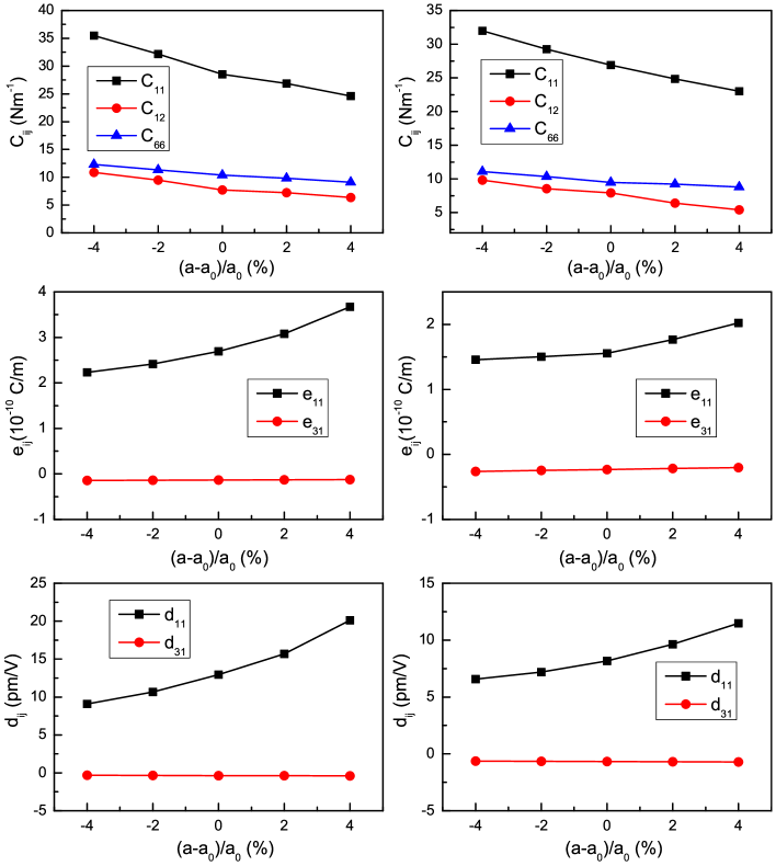
In general, a piezoelectric material should be a semiconductor for prohibiting current leakage, which has been proved from energy bands structures from Figure 2. The elastic stiffness coefficients of and of SbTeI and BiTeI monolayers are firstly calculated, and the shear modulus , Young’s modulus and Poisson’s ratio are attained from calculated ela , which are listed in Table 1. These elastic coefficients satisfy the Born criteria of 2D hexagonal structureela (¿0 and -)¿0, proving their mechanical stabilities. These values are obviously smaller than those of other 2D materials, like monolayer TMDsq7 ; q9 , which means that SbTeI and BiTeI monolayers are more flexible than other 2D materials. Therefore, they are very favorable for novel flexible piezotronics.
For , the nonprimitive orthorhombic unit cell is used as the computational unit cell. The calculated in-plane () of SbTeI monolayer are 2.69 C/m (12.95 pm/V), and 1.56 C/m (8.20 pm/V) for BiTeI monolayer. Their is much higher than that of the widely used bulk materialsaln ; aln-1 ; aln-2 ; aln-3 ; aln-4 like -quartz (=2.3 pm/V), wurtzite-AlN (=5.1 pm/V) and wurtzite-GaN (=3.1 pm/V), and are found to be comparable to or even superior than other 2D materialsq7 ; q9 ; q11 ; q12 ; q7-2 ; q7-1 , such as , , ZnO, MoSSe and MoSTe. The related data are listed Table 2. These imply that the SbTeI and BiTeI monolayers may have large in-plane piezoelectric effects with a uniaxial strain being applied.
For 2D materials, a large out-of-plane piezoelectric response is highly desired, since it is compatible with the nowadays bottom/top gate technologies. The calculated out-of-plane piezoelectric strain coefficient () has large value of -0.37 pm/V for SbTeI monolayer, and -0.66 pm/V for BiTeI monolayer. The out-of-plane piezoelectricity of BiTeI monolayer is obviously higher than ones of other 2D materials, like functionalized h-BN (0.13 pm/V)y1 , MoSSe (0.29 pm/V)q7-2 , MoSTe (0.4 pm/V)q7-1 , Janus group-III materials (0.46 pm/V)y2 and - (0.415 pm/V)y3 . It is noted that the and of MoSSe and MoSTe are very different between ref.q7 and ref.q7-2 ; q7-1 , which are likely due to different computational method. In ref.q7-2 ; q7-1 , the are calculated by DFPT, while these are attained by evaluating the change of unit-cell polarization after imposing small strain in ref.q7 . It is clearly seen that the are very close for different method, but the by polarization-strain relation is smaller by 1 order of magnitude compared to one by DFPT. The large out-of-plane piezoelectric effect makes SbTeI and BiTeI monolayers have potential applications on ultrathin piezoelectric devices.
| Carrier type | () | (eV) | () | (s) | |||
|---|---|---|---|---|---|---|---|
| Electrons | x | 26.43 | 0.21 | -3.61 | 739.74 | ||
| SbTeI | y | 26.43 | 0.36 | -4.24 | 311.70 | ||
| Holes | x | 26.43 | -1.86 | -2.99 | 34.97 | ||
| y | 26.43 | -0.50 | -2.06 | 272.59 | |||
| Electrons | x | 24.57 | 0.19 | -2.62 | 1319.24 | ||
| BiTeI | y | 24.57 | 0.52 | -3.04 | 351.18 | ||
| Holes | x | 24.57 | -1.36 | -2.06 | 102.92 | ||
| y | 24.57 | -0.57 | -1.66 | 376.58 |
It is found that the magnitude of the ionic contribution is larger than that of the electronic contribution. For monolayer SbTeI (BiTeI), the ionic contribution accounts for 83% (81%) of , and 100% [The contribution between ionic and electronic one is opposite.] (75%) of . The ionic contribution and electronic contribution to are listed in Table 3. Thus, it is very important for calculating the piezoelectric stress tensors to consider relaxed-ion, not clamped-ion (only electronic contribution). In fact, the real piezoelectric stress tensor (a relaxed-ion result) is the sum of ionic and electronic contributions.
V Carrier mobility
To evaluate the performance of monolayer SbTeI and BiTeI for great potential in piezoelectric and electronic application, the carrier mobilities of their electron/hole transport can be calculated by the deformation potential (DP) theory proposed by Bardeen and Shockleydp . In this theory, the expression of the carrier mobility of a 2D material () is given:
| (8) |
where , and are the electron charge, the reduced Planck constant and the Boltzmann constant; the and are temperature and effective mass in the transport direction, and is the average effective mass. The is the elastic modulus derived from elastic constants , and the relationship between them isela :
| (9) |
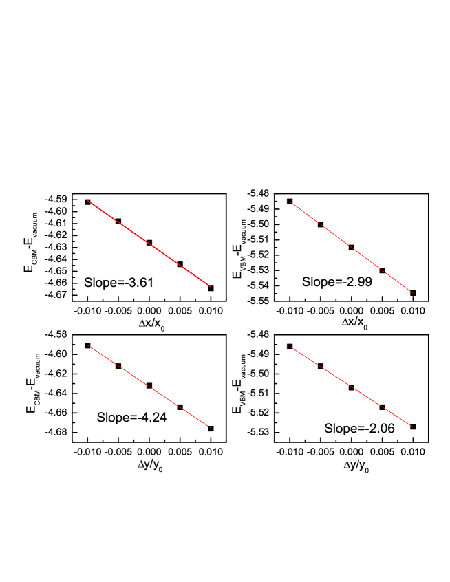
In addition, represents the DP constant of the VBM for a hole or the CBM for an electron along the transport direction, which is defined by , where is the energy shift of the band edge of CBM or VBM with respect to the vacuum level. These data are calculated with strain from -0.01 to 0.01, and the step =0.005. When the is attained, the relaxation time of a hole at VBM or an electron at CBM along the transport direction can be calculated by:
| (10) |
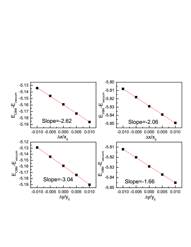
The rectangular supercell with armchair and zigzag being defined as x and y directions in Figure 1 is used to study the carrier mobilities of SbTeI and BiTeI monolayers, and the 300 K (room temperature) is used in the mobility calculations. It is noteworthy that calculating effective masses and the DP constant need consider SOC. Firstly, the effective masses of CBM and VBM along armchair and zigzag directions are calculated by:
| (11) |
In which is the dispersion of the lowest conduction band or the highest valence band. For both monolayer SbTeI and BiTeI, the calculated effective masses of electrons are smaller than ones of holes, and the effective masses along armchair direction are smaller than ones along zigzag direction for electrons, but that is opposite for holes. The band energies of the VBM and CBM with respect to the vacuum energy as a function of and are plotted in Figure 3 for SbTeI monolayer and in Figure 4 for BiTeI monolayer. The DP constant can be attained by linear fitting, and the related slopes are DP constant . Based on Equation 8, the carrier mobilities of SbTeI and BiTeI monolayers, including the electrons and holes along x and y directons, are calculated, and they are shown Table 4. The electron mobilities of monolayer SbTeI and BiTeI are in the range of 311.70-1319.24 , which are larger than those of holes (34.97-376.58 ). This mainly is because the effective masses of electron are smaller than ones of holes. Furthermore, the carrier mobilities between electrons and holes/between armchair and zigzag directions show very strong anisotropy. According to Equation 10, the can be calculated from effective masses and carrier mobilities, which is useful for attaining the electronic transport coefficients to study their electronic transport properties.
| Name | ||||
| SbTeI | 28.5 | 7.7 | 10.4 | 26.4 |
| BiTeI | 26.9 | 7.9 | 9.5 | 24.6 |
| 130.3 | 31.0 | 49.7 | 122.9 | |
| 146.0 | 31.6 | 57.2 | 139.2 | |
| 92.6 | 61.9 | 15.35 | 51.2 | |
| 126.8 | 27.4 | 49.7 | 120.9 | |
| 112.7 | 22.7 | 45 | 108.1 |
VI Discussions and Conclusion
From Table 2, the of Janus monolayer SbTeI and BiTeI are found to be comparable to or even smaller than ones of , , ZnO, MoSSe and MoSTeq7 ; q9 ; q7-2 ; q7-1 , but their are larger than ones of those 2D materials, except for ZnO. To find out underlying reasons, the elastic constants , shear modulus , Young’s modulus of Janus monolayer SbTeI and BiTeI along with ones of q9 , q9 , ZnOq9 , MoSSeq7 and WSTeq7 are listed in Table 5. Based on Equation 7, the is inversely proportional to [=()/2]. It is clearly seen that of Janus monolayer SbTeI and BiTeI are very smaller than ones of other 2D materials listed in Table 5, which leads to larger . It is also noted that of monolayer ZnO is relatively small, along with relatively large , which gives rise to large (8.65 pm/V). The is inversely proportional to (), and both and of Janus monolayer SbTeI and BiTeI are smaller than other ones from Table 5. Thus, the of Janus monolayer SbTeI and BiTeI are found to be smaller than ones of MoSSe and MoSTeq7-2 ; q7-1 using the same DFPT method, but their are comparable to or even larger than ones of MoSSe and MoSTe.
Strain is a very effective measures to tune the electronic, topological and transport properties of 2D materials. Here, we also investigate the small biaxial strain (-4% to 4%) effects on piezoelectric properties of monolayer SbTeI and BiTeI. The elastic constants , piezoelectric coefficients and of monolayer SbTeI and BiTeI as a function of strain are plotted in Figure 5. When the strain changes from -4% to 4%, all of both monolayer SbTeI and BiTeI show a monotone decrease, which is in favour of improving piezoelectric effects according to Equation 7. It is found that piezoelectric coefficient increases with strain from -4% to 4%, which leads to enhanced along with reduced . At 4% strain, the of SbTeI (BiTeI) reaches up to 20.12 pm/V (11.48 pm/V) from unstrained 12.95 pm/V (8.20 pm/V), increased by 55% (40%). Calculated results show that the or has small dependence on strain. For example, at 4% strain, the of SbTeI (BiTeI) becomes -0.41 pm/V (-0.71 pm/V) from unstrained -0.37 pm/V (-0.66 pm/V), enhanced by 11% (8%). A 2D material showing piezoelectricity should be a semiconductor, except breaking inversion symmetry. Calculated results show that they all are semiconductors in considered strain range. Thus, tensile strain can enhance piezoelectric effects of Janus monolayer SbTeI and BiTeI.
In summary, the electronic structures, piezoelectric properties and carrier mobilities of the Janus monolayer SbTeI and BiTeI are studied by using first-principles calculations. The inversion asymmetry together with the SOC effect give rise to Rashba-like splitting bands with an indirect band gap of 0.89 eV for SbTeI and 0.67 eV for BiTeI. The specific structural symmetry along with flexible mechanical properties induce large in-plane piezoelectric coefficient (=12.95 pm/V for SbTeI and =8.20 pm/V for BiTeI) and an additional out-of-plane piezoelectric coefficient (=-0.37 pm/V for SbTeI and =0.66 pm/V for BiTeI). Their carrier mobilities are attained with pronounced anisotropy, and the hole mobilities are higher than electron ones. The hole carrier mobility of the BiTeI monolayer along the armchair direction could be as high as 1319 . These findings can stimulate experimental works to explore piezoelectric and electronic applications of Janus monolayer SbTeI and BiTeI.
Acknowledgements.
This work is supported by the Natural Science Foundation of Shaanxi Provincial Department of Education (19JK0809). We are grateful to the Advanced Analysis and Computation Center of China University of Mining and Technology (CUMT) for the award of CPU hours and WIEN2k/VASP software to accomplish this work.References
- (1) C. Lee, X. D. Wei, J. W. Kysar and J. Hone, Science 321, 385 (2008).
- (2) H. L. Zhuang, R. G. Hennig, Phys. Rev. B 88, 115314 (2013).
- (3) H. Park, A. Wadehra, J. W. Wilkins and A. H. Castro Neto, Appl. Phys. Lett. 100, 253115 (2012).
- (4) W. Wu and Z. L. Wang, Nat. Rev. Mater. 1, 16031 (2016).
- (5) W. Wu, L. Wang, Y. Li, F. Zhang, L. Lin, S. Niu, D. Chenet, X. Zhang, Y. Hao, T. F. Heinz, J. Hone and Z. L. Wang, Nature 514, 470 (2014).
- (6) H. Zhu, Y. Wang, J. Xiao, M. Liu, S. Xiong, Z. J. Wong, Z. Ye, Y. Ye, X. Yin and X. Zhang, Nat. Nanotechnol. 10, 151 (2015).
- (7) L. Dong, J. Lou and V. B. Shenoy, ACS Nano, 11, 8242 (2017).
- (8) A. Y. Lu, H. Zhu, J. Xiao, C. P. Chuu, Y. Han, M. H. Chiu, C. C. Cheng, C. W. Yang, K. H. Wei, Y. Yang, Y. Wang, D. Sokaras, D. Nordlund, P. Yang, D. A. Muller, M. Y. Chou, X. Zhang and L. J. Li, Nat. Nanotechnol. 12, 744 (2017).
- (9) M. N. Blonsky, H. L. Zhuang, A. K. Singh and R. G. Hennig, ACS Nano, 9, 9885 (2015).
- (10) R. X. Fei, We. B. Li, J. Li and L. Yang, Appl. Phys. Lett. 107, 173104 (2015)
- (11) K. N. Duerloo, M. T. Ong and E. J. Reed, J. Phys. Chem. Lett. 3, 2871 (2012).
- (12) Y. Chen, J. Y. Liu, J. B. Yu, Y. G. Guo and Q. Sun, Phys. Chem. Chem. Phys. 21, 1207 (2019).
- (13) Y. Ma,Y.Dai,W.Wei, X. Li, and B. Huang, Phys. Chem. Chem. Phys. 16, 17603 (2014).
- (14) H. L. Zhuang, V. R. Cooper, H. X. Xu, P. Ganesh, R. G. Hennig and P. R. C. Kent, Phys. Rev. B 92, 115302 (2015).
- (15) S. D. Guo, A. X. Zhang and H. C. Li, Nanotechnology 28, 445702 (2017).
- (16) K. Tsubouchi and N. Mikoshiba, IEEE Trans. Sonics Ultrason. SU-32, 634 (1985).
- (17) C. M. Lueng, H. L. Chang, C. Suya and C. L. Choy, J. Appl. Phys. 88, 5360 (2000).
- (18) A. Hangleiter, F. Htzel, S. Lahmann and U. Rossow, Appl. Phys. Lett. 83, 1169 (2003).
- (19) S. Muensit, E. M. Goldys and I. L. Guy, Appl. Phys. Lett. 75, 3965 (1999).
- (20) R. Bechmann, Phys. Rev. 110, 1060 (1958).
- (21) P. Hohenberg and W. Kohn, Phys. Rev. 136, B864 (1964); W. Kohn and L. J. Sham, Phys. Rev. 140, A1133 (1965).
- (22) G. Kresse, J. Non-Cryst. Solids 193, 222 (1995).
- (23) G. Kresse and J. Furthmller, Comput. Mater. Sci. 6, 15 (1996).
- (24) G. Kresse and D. Joubert, Phys. Rev. B 59, 1758 (1999).
- (25) J. P. Perdew, K. Burke and M. Ernzerhof, Phys. Rev. Lett. 77, 3865 (1996).
- (26) X. Wu, D. Vanderbilt and D. R. Hamann, Phys. Rev. B 72, 035105 (2005).
- (27) R. Peng, Y. D. Ma, B. B. Huang and Y. Dai, J. Mater. Chem. A 7, 603 (2019).
- (28) R. C. Andrew, R. E. Mapasha, A. M. Ukpong and N. Chetty, Phys. Rev. B 85, 125428 (2012).
- (29) S. D. Guo and X. S. Guo, arXiv.1908.02908 (2019).
- (30) M. Yagmurcukardes, C. Sevik and F. M. Peeters, Phys. Rev. B 100, 045415 (2019).
- (31) A. A. M. Noor, H. J. Kim and Y. H. Shin, Phys. Chem. Chem. Phys. 16, 6575 (2014).
- (32) Y. Guo, S. Zhou, Y. Z. Bai, J. J. Zhao, Appl. Phys. Lett. 110, 163102 (2017).
- (33) L. Hu and X. R. Huang, RSC Adv. 7, 55034 (2017).
- (34) S. Bruzzone and G. Fiori, Appl. Phys. Lett. 99, 222108 (2011).