Superconducting proximity effect in InAsSb surface quantum wells with in-situ Al contacts
Abstract
We demonstrate a robust superconducting proximity effect in InAs0.5Sb0.5 quantum wells grown with epitaxial Al contacts, which has important implications for mesoscopic and topological superconductivity. Unlike more commonly studied InAs and InSb semiconductors, bulk InAs0.5Sb0.5 supports stronger spin-orbit coupling and a larger -factor. However, these potentially desirable properties have not been previously measured in epitaxial heterostructures with superconductors, which could serve as a platform for fault-tolerant topological quantum computing. Through structural and transport characterization we observe high-quality interfaces and strong spin-orbit coupling. We fabricate Josephson junctions based on InAs0.5Sb0.5 quantum wells and observe a strong proximity effect. With a contact separation of , these junctions exhibit products and of normal resistance , critical current , and excess current . Both of these quantities demonstrate a robust and long-range proximity effect with highly-transparent contacts.
A given material can be transformed through proximity effects whereby it acquires correlations from its neighbors, for example, becoming superconducting or magnetic. Such proximity effects not only complement the conventional methods of designing materials by doping or functionalization, but can also overcome their various limitations and enable novel states of matter 1. A striking example of this approach is semiconductors with strong spin-orbit coupling (SOC) and large -factor, in proximity to conventional superconductors. Such structures are predicted to support topological superconductivity with exotic quasi-particle excitations including Majorana bound states (MBS), which hold promise for fault-tolerant quantum computing Alicea_2012, 7. Through braiding (exchange) of MBS it is possible to reveal their peculiar non-Abelian statistics and implement fault-tolerant quantum gates 2.
Most efforts to realize MBS have been focused on one-dimensional (1D) systems, typically relying on proximitized InAs and InSb nanowires in an applied magnetic field. However, their geometry has inherent difficulties to implement braiding and imposes strong constraints on material parameters to achieve topological superconductivity, usually inferred from observation of a quantized zero-bias conductance peak. Instead, to overcome these limitations there is a growing interest in 2D platforms of proximitized semiconductors, which would also support topological superconductivity. These advantages have recently been demonstrated in planar Josephson junctions 3, 4, 5 where the phase transition between trivial and topological superconductivity can be tuned using gate voltages and the superconducting phase. This allows for more complicated networks that could support fusion, braiding, and large-scale Majorana manipulation.
The motivation to study InAs0.5Sb0.5 goes beyond proximity effects. In the past it was recognized as an important material for infrared applications 6, but there remains limited data available on quantum transport 7. More recently, the discovery of ultrafast lasers with spin-polarized carriers 8 calls for semiconductors with very short spin-relaxation times which is also expected from InAs0.5Sb0.5 considering its strong SOC.
To address this situation we use molecular beam epitaxy to fabricate high-quality 2D junctions of aluminum and InAs0.5Sb0.5. Our sample characterization and transport measurements in the normal and superconducting state are complemented by numerical analysis focusing on the role of the SOC and the quantum confinement which directly influence the resulting -factors. While most of the implications of our work are given in the context of a possible platform for realizing superconducting junctions that could support Majorana bounds states, we expect that the presented results could also motivate further work in elucidating the normal-state properties of InAs0.5Sb0.5 and its applications.
Our experiments on InAs0.5Sb0.5-based two-dimensional electron gas (2DEG) are accompanied by numerical studies of its electronic structure, Rashba SOC and -factor. From previous work, it is reported that InAs0.5Sb0.5 can exhibit significantly larger spin-splitting 7, compared to InAs or InSb in which transport properties have been extensively explored. The bulk -factor of InAs0.5Sb0.5 is expected to reach up to -120 and exhibit SOC almost an order of magnitude stronger than InAs 9. We find that the -factor is suppressed in narrow quantum wells, while the linear term in spin-orbit coupling decreases as quantum well width is increased.

We use a standard 8-band method 10 to calculate the subband structure of the surface InAs0.5Sb0.5 QW. The quantum confinement along the growth direction was addressed by using the finite difference method with a discretization step of which is sufficient to achieve convergence. For computational efficiency, we neglect the impact of the metal-semiconductor interface by modelling it as a hard-wall barrier acting as a confinement layer for the carriers. The material parameters were taken from Ref. 11 while the bowing parameter for the InAs0.5Sb0.5 alloy was taken from Ref. 12.
Since the system has broken inversion symmetry, the energy dispersion, , is spin-split due to the Rashba SOC. In Figure 1a we show the computed Rashba SOC parameter, , for the first conduction subband, computed as the linear slope of the energy difference very close to the -point 13. In order to understand the quantum confinement as well as the effect of the alloy composition, , we consider three InAs1-xSbx layer sizes and vary the composition from pure InAs to pure InSb. The gap at the InAs1-xSbx/In0.37Al0.63Sb interface is a broken one, i. e., the valence band edge is higher in energy than the conduction band edge and by increasing the InAs1-xSbx layer size the confined states’ energies cross each other. In this situation, no spin-splitting was computed since the conduction and valence subbands crossed. Furthermore, the trend that the smaller the InAs1-xSbx layer size, the larger the Rashba parameter is due to the fact that the electron has a higher probability to be found near the interfaces than in the middle of the layer. Indeed, as we reduce the InAs1-xSbx layer size the Rashba SOC parameter becomes larger. We found that the highest value is around for the InAs0.4Sb0.6 layer, for the InAs0.5Sb0.5 layer, and for the InAs0.6Sb0.4 layer. Our calculation does not include electrostatic self-consistency, and since Fermi-level pinning, which one can expect to be composition dependent, would increase the asymmetry of the structure 14, our calculation provides a minimum for the spin-orbit coupling strength, and may not capture its full composition dependence.
The -factor was computed using second order Löwdin partitioning 15, 16. In the bulk limit it converges to the Roth formula for an effective -factor,
| (1) |
where is the spin-orbit splitting of the valence bands and is the energy gap, while and are the free and effective electron masses, respectively. In Table 1, we show the bulk -factor for the In0.37Al0.63Sb barrier, InAs, InSb, and three selected InAs1-xSbx compositions. As we increase the composition, , the band gap of the material decreases and since the main contribution to the -factor comes from 16, we obtain the largest -factor values for compositions varying from to .
With quantum confinement, the -factor is typically lower than the corresponding bulk value. This trend can also be inferred from Eq. (1) since for a highly-confined system the effective band gap increases (as the energy difference from conduction to valence band also increases). We show the calculated -factor for a confined system along the growth direction, in Figure 1b, as well as perpendicular to the growth direction, in Figure 1c. Due to the quantum confinement and SOC, the -factor is anisotropic, i.e., , 17 with being larger in magnitude than . Moreover, following the trend of the Roth formula in Eq. (1), as we increase the size of the InAs1-xSbx layer, the -factor also increases. We found that the largest -factor occurs for a InAs0.4Sb0.6 QW and exceeds previous experimental results for a InSb QW which found in-plane and out-of-plane 18. The above calculations show that there is a sweet spot in terms of QW width where -factor and SOC are both strong. Motivated by this fact we focus the rest of our studies on 20 nm QWs.
| Compound | |
|---|---|
| In0.37Al0.63Sb | -4.65 |
| InAs | -14.61 |
| InAs0.6Sb0.4 | -70.86 |
| InAs0.5Sb0.5 | -99.08 |
| InAs0.4Sb0.6 | -116.82 |
| InSb | -49.23 |
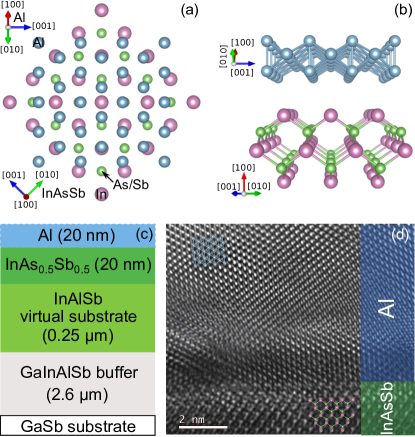
Molecular beam epitaxy (MBE) growth of large-area InAs0.5Sb0.5 surface QWs in epitaxial contact to aluminum films can form the basis for combining proximity effect with high -factor, strong SOC systems. Growth of semiconductor InAs0.5Sb0.5 is rather difficult since there is no insulating lattice-matched substrate immediately available. In this work, we pursue the process of compositional grading which allows growth of bulk unstrained, unrelaxed InAs0.5Sb0.5 of any composition onto GaSb, as previously reported 20, 21. Following earlier work, our samples have a GaInAlSb compositional grade followed by a In0.37Al0.63Sb virtual substrate (VS) and a InAs0.5Sb0.5 layer. Figure 2c shows a schematic of the layers, while Figure 2a shows a top view of the unstrained face-centered cubic Al lattice superimposed on the unstrained zincblende InAs0.5Sb0.5 lattice. We grew the sample by solid-source molecular beam epitaxy in a modular Gen II system with the As and Sb delivered by valved cracker sources. Except during the Al layer deposition, the substrate temperature was measured with a K-space BandiT system operating in pyrometry mode. Measurements of (004) triple-axis x-ray diffraction allowed us to verify the composition of the VS. We cannot examine the InAs0.5Sb0.5 layer, since it is too thin relative to the VS and the compositional grade, but test structures with thicker InAs0.5Sb0.5 layers were grown with this recipe and their composition was verified by X-ray diffraction.
For samples with Al, after the top InAs0.5Sb0.5 layer was grown, all shutters were closed and the sources were cooled to idling temperatures (around 300-400 ∘C). The residual gases were pumped overnight, allowing the background pressure in the chamber to reach the range. The next day, the sample was pointed towards the cryo-shroud for two hours and 40 minutes, allowing it to fall below . We deposited a layer of Al onto the InAs0.5Sb0.5 surface at a growth rate of . In this work, we present data from nominally identical structures, one with and one without an in-situ Al layer 22. Figure 2d shows a cross sectional transmission electron microscope image of the interface between the InAs0.5Sb0.5 and Al layers along the zone axis, while Figure 2b shows a 3D rendering of the interface from the same perspective. The substrate and InAs0.5Sb0.5 are oriented along a growth direction. The Al film consists of large domains predominately aligned along , tilted 4 degrees from the interfacial plane. The high resolution images of this region and numerous others show that the d-spacing of the growth direction planes is , corresponding to that for Al along . The orientation relationships of the crystal planes and the FFT pattern corresponds to Al examined at a zone axis with a growth direction.
We studied the magnetoresistance of the InAs0.5Sb0.5 surface 2DEG without Al in a van der Pauw geometry. Magnetotransport measurements were performed at using standard lock-in techniques and ac excitations – at frequencies below 100 Hz. We find mobilities of cm2/Vs at a carrier density .
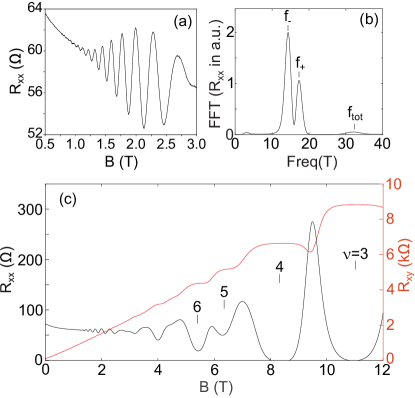
In the presence of strong SOC the Shubnikov-de Haas oscillations show two frequencies, signaling two Fermi surfaces, as can be seen in Figure 3a, which suggests occupation of two spin-subbands. Figure 3b shows the Fourier transform of these oscillations over the range. There are three clear peaks, which indicate spin-split subbands with frequencies = 17.2 T, = 14.2 T and a peak for the total frequency at = . The densities can be directly calculated from where is the electron charge and is Planck’s constant. We obtain and with which agrees with the Hall data shown in Figure 3c. This suggests the spin-split subband separation is very large as expected for InAs0.5Sb0.5. If this splitting were all due to the linear Rashba SOC term, we would obtain its parameter as , where , assuming a band mass of at 50% composition 23. Our calculation for this QW width predicts which is lower than the estimated from extracted parameters, suggesting there are contributions from Dresselhaus SOC terms in Sb compounds 24. We also note that a Schrödinger-Poisson calculation for our 20 nm QW showed one electronic subband is occupied.
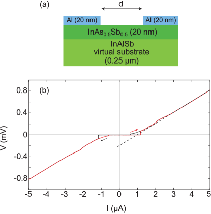
We further characterize the superconducting proximity effect in a Josephson junction (JJ) on an InAs0.5Sb0.5 2DEG with epitaxial Al contacts, as depicted schematically in Figure 4a. We fabricated Josephson junctions via electron beam lithography followed by selective wet etching (Transine type D) to remove a thin strip of Al. The junction is wide and has a length separation between the superconducting electrodes. Measurements were performed in a dilution fridge with a mixing chamber temperature of and an estimated electron temperature of . We used a 4-point measurement geometry and standard dc current bias techniques. The I-V characteristic of the junction is shown in Figure 4b. The voltage drop across the junction is zero (the supercurrent) up to a critical value of driving current denoted the critical current, .
The quality of the device can be characterized by a study of the and products, where is the normal resistance of the JJ. The excess current is the difference between the measured current through the junction and the expected current based on the junction’s . This occurs due to Andreev reflections and depends primarily on interface transparency. The critical current is the amount of current that can be carried by Andreev bound states through the junction with zero resistance. requires coherent charge transport across the semiconductor region and is therefore a measure of both interface transparency and 2DEG mobility.
The junction is neither clearly ballistic () nor diffusive () since the mean free path nm is of the order of the contact separation. The mean free path is obtained from the transport measurements in a van der Pauw geometry presented earlier. Using the diffusive expression for the Thouless energy with D the diffusion constant, we find . This value, which is likely underestimated since our junction is not deeply diffusive, is about 5 times larger than the superconducting gap eV which we extract from the BCS relation (see Supporting Information). As a consequence our junction is close to the short limit.
The Andreev process that carries the supercurrent across the Sm region is characterized by the induced gap in the Sm below the S, rather than the bulk Al gap, . To characterize an S-Sm-S junction in the short limit, the product of the critical current and the normal state resistance, which is related to the gap via , is often used, where is a constant of order unity. Experimentally, we find where , , in the junction with contact separation at T = 20 mK, consistent with previous results in InAsSb nanowires 7. The product of IcRN can be compared to theoretical values for fully transparent junctions in the short ballistic and short diffusive limits, for which is and , respectively 25. For our sample, we find is of the ballistic limit and of the diffusive limit. This results are comparable with what has been observed in InAs 2DEG for similar contact separations 26.
Due to the high mobility of the InAs0.5Sb0.5 channel he supercurrent persists at longer separations. At separation we still observe a substantial supercurrent with ; raw data is presented in the supplementary information.
High interface transparency corresponds to a high probability of Andreev reflection at the interface. Since the Sm extends under the S regions, the interface between Sm and S should be highly transparent due to the large area of contact and in-situ epitaxial Al growth 27. The Andreev process that carries supercurrent across the Sm region is characterized by the excess current through the junction. Excess current does not require coherent charge transport across the junction as it follows simply from charge conservation at the S-Sm interfaces. can be calculated by extrapolating from the high current normal regime to zero voltage as shown in Figure 4b with a dotted line. The excess current in our sample is found to be A.
When considering interface quality the more relevant quantity is the product . The product can be compared to the superconducting gap with the relation . In the case of a fully transparent S-Sm interface for a diffusive junction 28 and for a ballistic junction. For our sample, , which is close to values reported in InAs 2DEG 26. This value is of the ballistic limit and of the diffusive value for our 500 nm JJ. The Octavio–Tinkham–Blonder–Klapwijk theory allows to link the ratio to the interface transparency. Using equation (25) of Ref 29, we can extract the effective scattering parameter , leading to a 75% probability of Andreev reflection at zero energy. This value is similar to transparencies observed in InAs nanowires 30.
In conclusion, we have demonstrated a robust superconducting proximity effect in two-dimensional epitaxial Al-InAs0.5Sb0.5 systems. Using an optimized MBE growth we have achieved both high electron mobilities in InAs0.5Sb0.5 and successful epitaxial growth of thin film Al. Outstanding transport properties were confirmed in the normal and superconducting state by Shubnikov-de Haas oscillations and current-voltage measurements, which establish strong spin-orbit coupling and large critical current in Josephson junctions. Remarkably, the latter property, made possible by high interface transparency, is consistent with a large proximity-induced superconducting gap of eV in InAs0.5Sb0.5. The supercurrent between two Al contacts can be sustained in InAs0.5Sb0.5 across at least 1000 nm.
While these results clearly indicate that InAs0.5Sb0.5-based junctions provide a suitable platform in which to explore topological superconductivity, they also have broader implications. We expect that spin-orbit coupling in InAs0.5Sb0.5 could be further controlled through electrostatic gating or magnetic structures to modify quantum transport both in the normal and superconducting state.
Temperature dependence of supercurrent and products; Characterization of supercurrent in Josephson junction.
1 Acknowledgement
This work was partially supported by NSF DMR 1836687, the US Army research office, US ONR N000141712793, NSF ECCS-1810266, the University at Buffalo Center for Computational Research, and the ARO/LPS Quantum Computing Graduate Research Fellowship (QuaCGR BAA W911NF-17-S-0002).
2 Authors contributions
W.M, M.H. performed the measurements and analysis, J.Y. and M.C.D. helped with fabrication of the devices with J.S. providing input. K.S.W. and J.S. designed the stack. W.L.S and S.P.S grew the epitaxial Al/InAs heterostructures. A.C.L. performed TEM analysis. T.C. developed the simulation model and carried out the simulations. J.S. conceived the experiment. All authors contributed to interpreting the data. The manuscript was written by W.M, W.F.S., M.C.D., I.Ž., and J.S. with suggestions from all the other authors.
3 Notes
The authors declare no competing financial interest.
References
- Žutić et al. 2019 Žutić, I.; Matos-Abiague, A.; Scharf, B.; Dery, H.; Belashchenko, K. Proximitized materials. Materials Today 2019, 22, 85–107
- Aasen et al. 2016 Aasen, D.; Hell, M.; Mishmash, R. V.; Higginbotham, A.; Danon, J.; Leijnse, M.; Jespersen, T. S.; Folk, J. A.; Marcus, C. M.; Flensberg, K.; Alicea, J. Milestones Toward Majorana-Based Quantum Computing. Phys. Rev. X 2016, 6, 031016
- Mayer et al. 2019 Mayer, W.; Dartiailh, M. C.; Yuan, J.; Wickramasinghe, K. S.; Matos-Abiague, A.; Žutić, I.; Shabani, J. Phase signature of topological transition in Josephson Junctions. arXiv e-prints 2019, arXiv:1906.01179
- Fornieri et al. 2019 Fornieri, A. et al. Evidence of topological superconductivity in planar Josephson junctions. Nature 2019, 569, 89–92
- Ren et al. 2019 Ren, H.; Pientka, F.; Hart, S.; Pierce, A. T.; Kosowsky, M.; Lunczer, L.; Schlereth, R.; Scharf, B.; Hankiewicz, E. M.; Molenkamp, L. W.; Halperin, B. I.; Yacoby, A. Topological superconductivity in a phase-controlled Josephson junction. Nature 2019, 569, 93–98
- Piotrowski and Rogalski 2004 Piotrowski, J.; Rogalski, A. Uncooled long wavelength infrared photon detectors. Infrared Physics & Technology 2004, 46, 115–131
- Sestoft et al. 2018 Sestoft, J. E.; Kanne, T.; Gejl, A. N.; von Soosten, M.; Yodh, J. S.; Sherman, D.; Tarasinski, B.; Wimmer, M.; Johnson, E.; Deng, M.; Nygård, J.; Jespersen, T. S.; Marcus, C. M.; Krogstrup, P. Engineering hybrid epitaxial InAsSb/Al nanowires for stronger topological protection. Phys. Rev. Materials 2018, 2, 044202
- Lindemann et al. 2019 Lindemann, M.; Xu, G.; Pusch, T.; Michalzik, R.; Hofmann, M. R.; Žutić, I.; Gerhardt, N. C. Ultrafast spin-lasers. Nature 2019, 568, 212–215
- Winkler et al. 2016 Winkler, G. W.; Wu, Q.; Troyer, M.; Krogstrup, P.; Soluyanov, A. A. Topological Phases in : From Novel Topological Semimetal to Majorana Wire. Phys. Rev. Lett. 2016, 117, 076403
- Campos et al. 2019 Campos, T.; Sandoval, M. A. T.; Diago-Cisneros, L.; Sipahi, G. M. Electrical tuning of helical edge states in topological multilayers. Journal of Physics: Condensed Matter 2019, 31, 495501
- Vurgaftman et al. 2001 Vurgaftman, I.; Meyer, J. á.; Ram-Mohan, L. á. Band parameters for III–V compound semiconductors and their alloys. Journal of applied physics 2001, 89, 5815–5875
- Webster et al. 2015 Webster, P.; Riordan, N.; Liu, S.; Steenbergen, E.; Synowicki, R.; Zhang, Y.-H.; Johnson, S. Measurement of InAsSb bandgap energy and InAs/InAsSb band edge positions using spectroscopic ellipsometry and photoluminescence spectroscopy. Journal of Applied Physics 2015, 118, 245706
- Campos et al. 2018 Campos, T.; Junior, P. E. F.; Gmitra, M.; Sipahi, G. M.; Fabian, J. Spin-orbit coupling effects in zinc-blende InSb and wurtzite InAs nanowires: Realistic calculations with multiband k· p method. Physical Review B 2018, 97, 245402
- Betti et al. 2001 Betti, M. G.; Corradini, V.; Bertoni, G.; Casarini, P.; Mariani, C.; Abramo, A. Density of states of a two-dimensional electron gas at semiconductor surfaces. Phys. Rev. B 2001, 63, 155315
- Winkler 2003 Winkler, R. Spin-orbit Coupling Effects in Two-Dimensional Electron and Hole Systems; Physics and Astronomy Online Library 191; Springer, 2003
- Tadjine et al. 2017 Tadjine, A.; Niquet, Y.-M.; Delerue, C. Universal behavior of electron g-factors in semiconductor nanostructures. Physical Review B 2017, 95, 235437
- Sandoval et al. 2016 Sandoval, M. T.; e Silva, E. d. A.; da Silva, A. F.; La Rocca, G. Electron g factor anisotropy in asymmetric III–V semiconductor quantum wells. Semiconductor Science and Technology 2016, 31, 115008
- Qu et al. 2016 Qu, F.; van Veen, J.; de Vries, F. K.; Beukman, A. J. A.; Wimmer, M.; Yi, W.; Kiselev, A. A.; Nguyen, B.-M.; Sokolich, M.; Manfra, M. J.; Nichele, F.; Marcus, C. M.; Kouwenhoven, L. P. Quantized Conductance and Large g-Factor Anisotropy in InSb Quantum Point Contacts. Nano Letters 2016, 16, 7509–7513, PMID: 27805409
- Momma and Izumi 2011 Momma, K.; Izumi, F. VESTA3 for three-dimensional visualization of crystal, volumetric and morphology data. Journal of Applied Crystallography 2011, 44, 1272–1276
- Svensson et al. 2012 Svensson, S. P.; Sarney, W. L.; Hier, H.; Lin, Y.; Wang, D.; Donetsky, D.; Shterengas, L.; Kipshidze, G.; Belenky, G. Band gap of InAs1-xSbx with native lattice constant. Phys. Rev. B 2012, 86, 245205
- Belenky et al. 2011 Belenky, G.; Donetsky, D.; Kipshidze, G.; Wang, D.; Shterengas, L.; Sarney, W. L.; Svensson, S. P. Properties of unrelaxed InAs1−XSbX alloys grown on compositionally graded buffers. Applied Physics Letters 2011, 99, 141116
- Sarney et al. 2018 Sarney, W. L.; Svensson, S. P.; Wickramasinghe, K. S.; Yuan, J.; Shabani, J. Reactivity studies and structural properties of Al on compound semiconductor surfaces. Journal of Vacuum Science & Technology B 2018, 36, 062903
- Suchalkin et al. 2016 Suchalkin, S.; Ludwig, J.; Belenky, G.; Laikhtman, B.; Kipshidze, G.; Lin, Y.; Shterengas, L.; Smirnov, D.; Luryi, S.; Sarney, W. L.; Svensson, S. P. Electronic properties of unstrained unrelaxed narrow gap InAsxSb1−xalloys. 2016, 49, 105101
- Dedigama et al. 2008 Dedigama, A. R.; Jayathilaka, D.; Gunawardana, S. H.; Murphy, S. Q.; Edirisooriya, M.; Goel, N.; Mishima, T. D.; Santos, M. B. Measurement of the Dresselhaus and Rashba Spin-Orbit Coupling Via Weak Anti-Localization in InSb Quantum Wells. Narrow Gap Semiconductors 2008, 35–38
- Likharev 1979 Likharev, K. K. Superconducting Weak Links. Rev. Mod. Phys. 1979, 51, 101
- Mayer et al. 2019 Mayer, W.; Yuan, J.; Wickramasinghe, K. S.; Nguyen, T.; Dartiailh, M. C.; Shabani, J. Superconducting proximity effect in epitaxial Al-InAs heterostructures. Applied Physics Letters 2019, 114, 103104
- Kjaergaard et al. 2016 Kjaergaard, M.; Nichele, F.; Suominen, H. J.; Nowak, M. P.; Wimmer, M.; Akhmerov, A. R.; Folk, J. A.; Flensberg, K.; Shabani, J.; Palmstrøm, C. J.; Marcus, C. M. Quantized conductance doubling and hard gap in a two-dimensional semiconductor–superconductor heterostructure. Nature Communications 2016, 7, 12841 EP –
- Kulik and Omelyanchuk 1975 Kulik, I. O.; Omelyanchuk, A. N. Contribution to the microscopic theory of the Josephson effect in superconducting bridges. JETP Lett. 1975, 21, 96
- Niebler et al. 2009 Niebler, G.; Cuniberti, G.; Novotný, T. Analytical calculation of the excess current in the Octavio–Tinkham–Blonder–Klapwijk theory. Supercond. Sci. Technol. 2009, 22, 085016
- Gharavi et al. 2017 Gharavi, K.; Holloway, G. W.; LaPierre, R. R.; Baugh, J. Nb/InAs nanowire proximity junctions from Josephson to quantum dot regimes. Nanotechnology 2017, 28, 085202