Valley filters, accumulators and switches induced in graphene quantum dots by lines of adsorbed hydrogen atoms
Abstract
We present electronic structure and quantum transport calculations that predict conducting channels induced in graphene quantum dots by lines of adsorbed hydrogen atoms to function as highly efficient, experimentally realizable valley filters, accumulators and switches. The underlying physics is a novel property of graphene Dirac point resonances (DPRs) that is revealed here, namely, that an electric current passing through a DPR-mediated conducting channel in a given direction is carried by electrons of only one of the two graphene valleys. Our predictions apply to lines of hydrogen atoms adsorbed on graphene quantum dots that are either free standing or supported on a hexagonal boron nitride substrate.
I Introduction
Graphene is a two dimensional material whose conduction (valence) band possesses two valleys, i.e., minima (maxima) at the same energy but with differing momenta. Consequently, graphene is attracting attention as a possible platform for valleytronics, where the electron’s valley index is to be exploited as a further degree of freedom. In terms of the correspondence between the principal elements of spintronics and valleytronics, the potential importance of valley filters in valleytronics is evident, in view of the decisive role of spin filters in spintronics. Valley filtering mechanisms have been proposed based on topological considerations,XiaoPRL ; XiaoReview ; pan2015perfect transport through nano-constrictions,rycerz2007valley graphene line defects,gunlycke2011graphene ; Chen14 ; Ingaramo ; Cheng disorder,Cresti16 ; An opticalabergel2009generation ; Golub ; Kundu ; Lago2017 ; Qu2018 or thermalChenthermal ; Zhang2018 effects, electrostatic potentials,Costa15 ; wang2017valley ; Ang2017 monolayer-bilayer graphene boundaries,Nakanishi electron injection into graphene with broken inversion symmetry,george ; azari2017gate mirror symmetry breaking,Asmar substrate defects,daCosta p-n junctions,Sekera ; Park2018 grain boundaries, Nguyen16 strainsZhangstrained ; Settnesstrained ; Faraj2017 nanobubbles Settnes16 ; Munoz2017 and SiC nanoribbon junctions Zheng2017 . Interest in this topic is intense and growing rapidly at present.XiaoPRL ; rycerz2007valley ; abergel2009generation ; Nakanishi ; XiaoReview ; gunlycke2011graphene ; Chen14 ; Ingaramo ; pan2015perfect ; Costa15 ; Chenthermal ; george ; azari2017gate ; Nguyen16 ; Settnes16 ; Golub ; Kundu ; Cheng ; Cresti16 ; An ; Asmar ; Munoz2017 ; daCosta ; Zhangstrained ; Settnesstrained ; Sekera ; wang2017valley ; Lago2017 ; Ang2017 ; Faraj2017 ; Qu2018 ; Zhang2018 ; Park2018 ; Zheng2017
An obstacle to further progress is that well controlled, reproducible experimental realization of many of the proposed nanoscale devices is challenging. In this respect, nanostructures defined by arrays of atoms or molecules adsorbed on graphene may offer an attractive alternative since precisely defined patterns of adsorbed atoms can be produced to specification on surfaces with scanning tunneling microscopes.Eigler1990 ; Crommie1993 ; Hla In particular, positioning of adsorbed hydrogen atoms on graphene with atomic precision has been demonstrated.gonzalez2016atomic Adsorbed hydrogen modifies the electronic properties of grapheneSofo2007 ; Boukhvalov2008 ; Elias2009 ; Soriano2011 and endows it with new functionalities that may find applications in future technologies.Pumera2013 ; Ferrari2015 ; Jiang2018 However, valley filtering in graphene by means of adsorbed hydrogen (or other adsorbed species) has not been explored to date either experimentally or theoretically. Here we propose a novel, efficient, experimentally realizable mechanism of valley filtering in monolayer graphene quantum dots decorated by a double line of hydrogen atoms as depicted in Fig. 1. This new mechanism exploits scattering resonances induced in the graphene at energies near the Dirac point by adsorbed atomsRobinson08 ; Wehling09X ; Wehling09 ; Wehling10 ; ihnatsenka2011dirac ; Saffarzadeh12 ; ReviewRibbon ; Irmer18 and other defects.Skrypnyk06 ; Wehling07 ; Pereira08 ; Basko08 These “Dirac point resonances” are due to coupling between discrete states and the graphene continuum, as in Fano interference phenomena.Fano ; ihnatsenka2011dirac For the graphene quantum dots that we consider we find the hydrogen Dirac point resonances to fall within a quantum confinement-induced energy gap. Thus the hydrogen lines behave as a quasi-1D conductor with conduction mediated by Dirac point resonances. Our quantum transport calculations reveal that electrons belonging to the two graphene valleys travel in opposite directions along this 1D conductor. Thus an electric current flowing in a given direction through this conductor is carried by electrons belonging to just one of the graphene valleys. If the direction of the electric current is reversed, conduction switches to the other valley. Furthermore the electric current results in strong valley accumulation along the hydrogen lines. The electronic states involved are localized exponentially to the vicinity of the hydrogen lines. Thus we expect impurities and other imperfections located more than a few lattice spacings from the hydrogen lines not to degrade significantly the highly efficient operation of this novel nanoscale electrically controlled valley filter, accumulator and switch.
The paper is organized as follows. In Sec. II, we present the model that we use to describe the graphene quantum dot and adsorbed hydrogen. In Sec. III, we present the results of our calculations of the electrical conductance of the graphene quantum dot with and without adsorbed hydrogen, and with and without a symmetry-breaking substrate. In Sec. IV we present electronic band structure calculations for graphene ribbons with double lines of adsorbed hydrogen. With the help of the calculated band structures, we then interpret the results of our conductance calculations physically and relate the conductance features that we have found to valley filtering. In Sec. V we present our results for the electron valley filtering and the valley accumulations induced in the graphene dot near the hydrogen lines when an electric current flows through this system. Our conclusions are summarized in Sec. VI.
II The Model
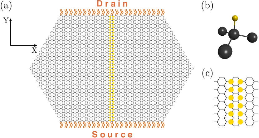
In Fig.1 (a), (c) the double line of hydrogen atoms (yellow disks) is oriented in the y-direction. The electron source and drain contacts that connect the quantum dot to the reservoirs are modeled as groups of semi-infinite 1D ideal leads (orange wavy lines). The geometry of a hydrogen atom adsorbed on graphene is shown in Fig.1 (b). The hydrogen and carbon atom to which hydrogen binds are 1.47 and 0.32Å above the graphene plane.ihnatsenka2011dirac
To model the nanostructure in Fig.1(a), we have used a tight-binding Hamiltonian that accurately describes the Dirac point resonances of hydrogen on graphene:ihnatsenka2011dirac
| (1) |
The first two terms are the well known nearest-neighbour tight-binding Hamiltonian of graphene. is the on-site energy of the carbon atoms. The third term is the on-site energy of adsorbed hydrogen atoms. The last term represents the hopping between the hydrogen and the carbon atom to which the hydrogen binds. The parameters are taken from Table I of Ref.ihnatsenka2011dirac, . As is discussed in Sections VI and VII of Ref.ihnatsenka2011dirac, , the values of were chosen so as to accurately describe the scattering of graphene electrons by the bonded hydrogen/carbon complex, including the effects of the carbon , and valence orbitals, and agree with the results of DFT calculations Wehling10 . As well as hydrogen on pristine graphene (the case ), we also consider hydrogen on graphene with broken inversion symmetry in each unit cell, (as in graphene on h-BN) with eV.George11 In that case, and , the site energies for carbon atoms under right and left hand lines of H atoms, have the opposite signs, breaking the left-right mirror symmetry of the nanostructure.
III Conductance Calculations
To explore the effects of the hydrogen lines on electron transport, we have carried out 2-terminal conductance calculations using a fully quantum mechanical approach within Landauer theory. According to the Landauer formula of electron transport, the electrical conductance at zero temperature in the linear response regime isEcon81 ; Fish81 ; ReviewRibbon
| (2) |
where and is the transmission probability of electron from lead in the source contact to lead in the drain contact at the Fermi energy . We calculate by solving the Lippmann-Schwinger equation for electron scattering through the nanostructure as is explained in detail in Appendix A of Ref. azari2017gate, .
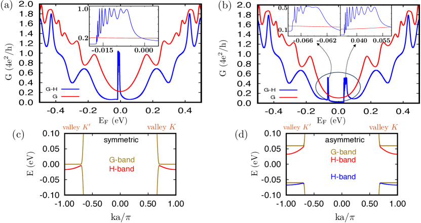
The calculated 2-terminal conductances [Eq.2] of the quantum dot in Fig.1(a) for the symmetric () and asymmetric () cases are shown in Fig.2 (a) and (b), respectively. The results for the graphene quantum dots with and without the hydrogen lines present are shown in blue and red. The calculated conductances for the symmetric and asymmetric cases are almost identical if the Fermi energy is far from zero. However, if the hydrogen lines are present, they differ markedly for Fermi energies around zero. In the symmetric case (blue curve, Fig.2 (a)), a striking enhancement of the conductance to occurs when the Fermi energy lies in the range . For the same model parameters, the Dirac point resonance for a single hydrogen atom on graphene is centered at eVihnatsenka2011dirac , which is in this range. This suggests that the conductance enhancement for Fermi energies around zero is due to transmission of electrons from the source to the drain mediated by Dirac point resonances of the individual hydrogen atoms which together induce a conducting channel across the quantum dot. We then attribute the series of conductance maxima and minima in the range seen in the inset of Fig.2 (a) to multiple reflections of electrons in this channel at the ends of the lines of hydrogen atoms. The much smaller conductance near zero energy in the absence of hydrogen (shown in red in Fig.2(a)) is due to quantum tunneling in the energy gap around zero energy that results from quantum confinement due to the finite size of the pristine graphene quantum dot. If the mirror symmetry is broken with respect to the hydrogen lines by modifying the on-site energies of carbon atoms as discussed above, two peaks (with differing fine structures) occur near and -0.06 eV, as shown by the blue curve and insets in Fig.2(b).
IV The Role of Band Structure
To clarify the underlying physics, in Fig.2 (c) and (d) we have plotted the band structures of infinite uniform graphene nanoribbons with and without double lines of adsorbed hydrogen atoms. The lines of hydrogen atoms on the ribbons are infinite, run along the centers of the ribbons, and are oriented in the -direction, as in Fig.1. This implies that the ribbons have zigzag edges. As is seen in Fig.2 (c), the presence of the hydrogen lines in the mirror symmetric case results in a four-fold degenerate (including spin) narrow band close to zero energy (red) in addition to the flat band at zero energynakada1996edge ; fujita1996peculiar (taupe colored) that is due to the zigzag ribbon edges. Fig.2 (d) shows that breaking the mirror symmetry (with ) opens a band gap of width around zero energy, splitting both the flat band due to the zigzag edges (taupe) and the band due to the hydrogen (red and blue). It is evident that states of these hydrogen-induced bands give rise to the conductance peaks near the Dirac point in Fig.2 (a) and (b). Note that there are no features due to zigzag edges in the conductance plots in Fig.2(a) and (b) because the quantum dots considered there have only armchair edges as in Fig. 1.
In Fig.2 (c) and (d) the hydrogen-induced bands have positive (negative) velocities for negative (positive) values of that can be regarded as projections of valley () on the -axis. [ and are defined in the insets of Fig.3. The corresponding ribbon values are indicated at the top of Fig.2 (c),(d)]. This suggests that H-band electrons traveling in the positive (negative) -direction in Fig.1 belong to valley (). Consequently, the Dirac point resonance states induced by the lines of H-atoms should function as an effective valley filter. Also an electric current mediated by the Dirac point resonances [i.e., for at a conductance peak near the Dirac point in Fig.2(a) and (b)] should induce a strong valley polarization near the adsorbed hydrogen lines. These heuristic ideas are fully confirmed by our calculations of the valley accumulations induced by electric currents that we present next.
V Valley Filtering and Valley Accumulation
To this end, we have solved the Lippmann-Schwinger equation to find the electronic scattering eigenstates of the coupled system (graphene-hydrogen and leads) in Fig. 1. These scattering eigenstates were then projected onto the Bloch states belonging to the two graphene valleys. (Our method of solving Lippmann-Schwinger equations and carrying out valley projections is explained in Appendices A and B of Ref.azari2017gate, ). Then for a nanostructure with two contacts each at a specific electrochemical potential , , the current-induced electron accumulation in valley calculated at atomic site is given byazari2017gate :
| (3) |
where , are the projections of the scattering state on the valleys and , is the atomic orbital at site , and is the electrochemical potential difference between contact and the contact with the lowest electrochemical potential. Here the scattering state emanates from semi-infinite 1D ideal lead represented by a tight-binding chain such that on site of the chain where is the reflection amplitude of the incoming state from the nanostructure back into ideal lead , and is the energy eigenvalue corresponding to state .
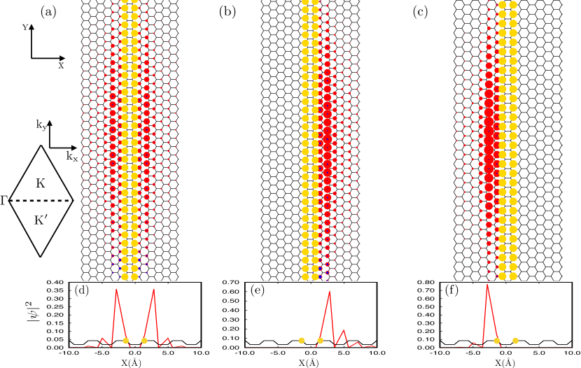
Representative examples of the calculated spatial distributions of the current-induced electron accumulations and in valleys and near the double hydrogen line in Fig. 1 are shown as blue and red disks, respectively, in Fig.3 (a-c). The disk diameters are proportional to . In each case shown, the Fermi level is in a hydrogen-induced band of states, i.e., a H-band of Fig.2 (c) or (d). The results for the symmetric () case are in Fig.3 (a). Those for the asymmetric () case are in Fig.3 (b) and (c) for in the upper and lower H-band respectively. In each case the electron flow is in the positive -direction. In all cases the accumulation is overwhelmingly in the valley (red disks dominate), as is predicted by our heuristic reasoning presented above. I.e., electron flow in the positive -direction is due to valley electrons for which the velocity in the H-bands in Fig.2 is positive. We attribute the much smaller population of valley electrons (blue disks) to the minority of electrons traveling in the negative -direction after partial reflection at the upper ends of the hydrogen lines in Fig.1. If we define the valley filter efficiency as the current-induced valley polarization , then we find efficiencies of 90.8 in Fig.3(a) [symmetric case], and 91.8 and 95.1 in Fig.3(b) and (c) [asymmetric cases], respectively. It is possible to tune the filter efficiency by modifying conditions so as to vary the electron reflection probability. For example, locating in a broader conductance peak (in an inset of Fig.2 (a) or (b)) lowers the reflection probability and, accordingly, lowers the valley electron accumulation and raises the filter efficiency. The calculated wave function distributions over the unit cell of a graphene nanoribbon with a double hydrogen line, Fig.3 (d-f), confirms that the hydrogen-induced states are exponentially localized around the hydrogen lines in a similar way to the corresponding valley accumulations in Fig.3 (a-c).
In all of the above cases the valley filtering allows transport of valley electrons while excluding almost all valley electrons. However, if the direction of the electric current is reversed, the filtering switches to favoring valley instead of valley . It should be noted that, this novel valley filtering mechanism only operates at the energies of the hydrogen-induced Dirac point resonance bands. It does not function if the Fermi energy is far from the Dirac point resonances.
VI Conclusions
In conclusion, the present work has revealed an efficient, experimentally realizable valley filtering mechanism that exploits in a novel way the Dirac point resonances due to arrays of hydrogen atoms adsorbed on graphene quantum dots. We have shown that a double row of adsorbed hydrogen atoms induces an electrically conducting channel in the graphene for Fermi energies near the Dirac point and within the quantum confinement-induced energy gap of the corresponding pristine graphene quantum dot. We predict that an electric current passing through the channel in a given direction is carried by electrons of only one of the two graphene valleys. If the direction of the current is reversed, conduction switches to electrons of the other valley. This novel valley filtering mechanism applies for hydrogen adsorbed on pristine graphene and also on graphene whose symmetry is broken by a h-BN substrate. We have shown that if electron reflection at the ends of the channel is minimized, electrons belonging almost entirely to just one graphene valley accumulate in a nanometer-wide region along the conducting channel. Thus we have proposed here a novel, efficient valley filter, accumulator and switch.
Acknowledgements.
This work was supported by NSERC, Westgrid, CIFAR, and Compute Canada.References
- (1) D. Xiao, W. Yao, Q. Niu, Valley-Contrasting Physics in Graphene: Magnetic Moment and Topological Transport, Phys. Rev. Lett. 99, 236809 (2007).
- (2) D. Xiao, M.-C. Meng, Q. Niu, Berry phase effects on electronic properties, Rev. Mod. Phys. 82, 1959 (2010).
- (3) H. Pan, X. Li, F. Zhang, and S.A. Yang, Perfect valley filter in a topological domain wall, Phys. Rev. B 92, 041404 (2015).
- (4) A. Rycerz, J. Tworzydło, and C. W. J. Beenakker, Valley filter and valley valve in graphene, Nature Phys. 3, 172 (2007).
- (5) D. Gunlycke and C. T. White, Graphene valley filter using a line defect, Phys. Rev. Lett. 106, 136806 (2011).
- (6) J.-H. Chen, G. Autès, N. Alem, F. Gargiulo, A. Gautam, M. Linck,C. Kisielowski, O. V. Yazyev, S. G. Louie, and A. Zettl, Controlled growth of a line defect in graphene and implications for gate-tunable valley filtering, Phys. Rev. B89, 121407(R) (2014).
- (7) L. H. Ingaramo and L. E. F. Foa Torres, Valley filtering by a line-defect in graphene: quantum interference and inversion of the filter effect, J. Phys.: Condens. Matter 28, 485302 (2016).
- (8) S.-g. Cheng, J. Zhou, H. Jiang, Q.-F. Sun, The valley filter efficiency of monolayer graphene and bilayer graphene line defect model, New J. Phys. 18, 103024 (2016).
- (9) A. Cresti, B. K. Nikolić, J. H. García, S. Roche, Charge, spin and valley Hall effects in disordered graphene, Rivista Del Nuovo Cimento, 39, 587 (2016).
- (10) X.-T. An, J. Xiao, M.W.-Y. Tu, H. Yu, V. I. Fal ko, and W. Yao, Realization of Valley and Spin Pumps by Scattering at Nonmagnetic Disorders Phys. Rev. Lett. 118, 096602 (2017)
- (11) D. S. L. Abergel and T. Chakraborty, Generation of valley polarized current in bilayer graphene, Appl. Phys. Lett. 95, 041404 (2009).
- (12) L. E. Golub, S. A. Tarasenko, M. V. Entin and L. I. Magarill, Valley separation in graphene by polarized light, Phys. Rev. B84, 195408 (2011).
- (13) A. Kundu, H. A. Fertig, and B. Seradjeh, Floquet-Engineered Valleytronics in Dirac Systems, Phys. Rev. Lett. 116, 016802 (2016).
- (14) V. D. Lago, E. S. Morell, L.E.F.F. Torres, One-way transport in laser-illuminated bilayer graphene: A Floquet isolator, Phys. Rev. B96, 235409 (2017).
- (15) C. Qu, C. Zhang, F. Zhang, Valley-selective topologically ordered states in irradiated bilayer graphene, 2D Materials 5, 011005 (2018).
- (16) X. Chen, L. Zhang, and H. Guo, Valley caloritronics and its realization by graphene nanoribbons, Phys. Rev. B 92, 155427 (2015).
- (17) L. Zhang, Z. Yu, F. Xu, J. Wang, Influence of dephasing and B/N doping on valley Seebeck effect in zigzag graphene nanoribbons, Carbon 126, 183 (2018).
- (18) D. R. da Costa, A. Chaves, S. H. R. Sena, G. A. Farias and F. M. Peeters, Valley filtering using electrostatic potentials in bilayer graphene, Phys. Rev. B92, 045417 (2015).
- (19) J. J. Wang, S. Liu, J. Wang, and F. L. Liu,Valley filter and valve effect by strong electrostatic potentials in graphene, Sci. Rep. 7, 10236 (2017).
- (20) Y.S. Ang, S.A. Yang, C. Zhang, Z. Ma, L.K. Ang, Valleytronics in merging Dirac cones: All-electric-controlled valley filter, valve, and universal reversible logic gate, Phys. Rev. B96, 245410 (2017).
- (21) T. Nakanishi, M. Koshino, and T. Ando, Transmission through a boundary between monolayer and bilayer graphene, Phys. Rev. B82, 125428 (2010).
- (22) G. Kirczenow, Valley currents and nonlocal resistances of graphene nanostructures with broken inversion symmetry from the perspective of scattering theory, Phys. Rev. B 92, 125425 (2015).
- (23) M. Azari, and G. Kirczenow, Gate-tunable valley currents, non-local resistances and valley accumulation in bilayer graphene nanostructures, Phys. Rev. B 95, 195424 (2017).
- (24) M. M. Asmar and S. E. Ulloa, Minimal geometry for valley filtering in graphene, Phys. Rev. B96, 201407(R) (2017).
- (25) D. R. da Costa, A. Chaves, G. A. Farias and F. M. Peeters, Valley filtering in graphene due to substrate-induced mass potential, J. Phys.: Condens. Matter 29, 215502 (2017).
- (26) T. Sekera, C. Bruder, E. J. Mele,and R. P. Tiwari, Switchable valley filter based on a graphene p-n junction in a magnetic field, Phys. Rev. B95, 205431 (2017).
- (27) C.-S. Park, Valley filtering due to orbital magnetic moment in bilayer graphene, Phys. Lett. A 382, 121 (2018).
- (28) V. H. Nguyen, S. Dechamps, P. Dollfus, and J.-C. Charlier, Valley Filtering and Electronic Optics Using Polycrystalline Graphene, Phys. Rev. Lett. 117, 247702 (2016).
- (29) X.-P. Zhang, C. Huang and M. A Cazalilla, Valley Hall effect and nonlocal transport in strained graphene, 2D Mater. 4, 024007 (2017)
- (30) M. Settnes J. H. Garcia and S. Roche, Valley-polarized quantum transport generated by gauge fields in graphene, 2D Mater. 4, 031006 (2017)
- (31) T. Farajollahpour, A. Phirouznia, The role of the strain induced population imbalance in valley polarization of graphene: Berry curvature perspective, Scientific Reports 7, 17878 (2017).
- (32) M. Settnes, S. R. Power, M. Brandbyge, and A.-P. Jauho, Graphene Nanobubbles as Valley Filters and Beam Splitters, Phys. Rev. Lett. 117, 276801 (2016).
- (33) E. Muñoz, R. Soto-Garrido, Analytic approach to magneto-strain tuning of electronic transport through a graphene nanobubble: perspectives for a strain sensor, J. Phys.: Condens. Matter 29, 445302 (2017).
- (34) X. Zheng, X. Chen, L. Zhang, L. Xiao, S. Jia, Z. Zeng and H. Guo, Perfect spin and valley polarized quantum transport in twisted SiC nanoribbons, 2D Mater. 4, 025013 (2017).
- (35) D. M. Eigler and E. K. Schweizer, Positioning single atoms with a scanning tunnelling microscope, Nature 344, 524 (1990).
- (36) M. F. Crommie, C. P. Lutz, D. M. Eigler, Confinement of Electrons to Quantum Corrals on a Metal Surface, Science 262, 218 (1993).
- (37) S. W. Hla, Atom-by-atom assembly, Rep. Prog. Phys. 77, 056502 (2014).
- (38) H. Gonzalez-Herrero, J. M. Gomez-Rodriguez, P. Mallet, M. Moaied, J. J. Palacios, C. Salgado, M. M. Ugeda, J.-Y. Veuillen, F. Yndurain, and I. Brihuega, Atomic-scale control of graphene magnetism by using hydrogen atoms, Science 352, 437 (2016).
- (39) J. O. Sofo, A. S. Chaudhari, and G. D. Barber, Graphane: A two-dimensional hydrocarbon, Phys. Rev. B75, 153401 (2007).
- (40) D. W. Boukhvalov, M. I. Katsnelson, and A. I. Lichtenstein, Hydrogen on graphene: Electronic structure, total energy, structural distortions and magnetism from first-principles calculations, Phys. Rev. B77, 035427 (2008).
- (41) D. C. Elias, R. R. Nair, T. M. G. Mohiuddin, S. V. Morozov, P. Blake, M. P. Halsall, A. C. Ferrari, D. W. Boukhvalov, M. I. Katsnelson, A. K. Geim, K. S. Novoselov, Control of Graphene s Properties by Reversible Hydrogenation: Evidence for Graphane, Science 323, 610 (2009).
- (42) D. Soriano, N. Leconte, P. Ordejón, J.-C. Charlier, J.-J. Palacios, and S. Roche, Magnetoresistance and Magnetic Ordering Fingerprints in Hydrogenated Graphene, Phys. Rev. Lett.107, 016602 (2011).
- (43) M. Pumera and C. H. A. Wong, Graphane and hydrogenated graphene, Chem. Soc. Rev., 42, 5987 (2013).
- (44) A. C. Ferrari, F. Bonaccorso, V. Fal ko, K. S. Novoselov, S. Roche, P. Bøggild, S. Borini, F. H. L. Koppens, V. Palermo, N. Pugno, J. A. Garrido, R. Sordan, A. Bianco, L. Ballerini, M. Prato, E. Lidorikis, J. Kivioja, C. Marinelli, T. Ryhäen, A. Morpurgo, J. N. Coleman, V. Nicolosi, L. Colombo, A. Fert, M. Garcia-Hernandez, A. Bachtold, G. F. Schneider, F. Guinea, C. Dekker, M. Barbone, Z. Sun, C. Galiotis, A. N. Grigorenko, G. Konstantatos, A. Kis, M. Katsnelson, L. Vandersypen, A. Loiseau, V. Morandi, D. Neumaier, E. Treossi, V. Pellegrini, M. Polini, A. Tredicucci, G. M. Williams, B. Hee Hong, J.-H. Ahn, J. M. Kim, H. Zirath, B. J. van Wees, H. van der Zant, L. Occhipinti, A. Di Matteo, I. A. Kinloch, T. Seyller, E. Quesnel, X. Feng, K. Teo, N. Rupesinghe, P. Hakonen, S. R. T. Neil, Q. Tannock, T. Löfwander and J. Kinaret, Science and technology roadmap for graphene, related two-dimensional crystals, and hybrid systems, Nanoscale, 7, 4598 (2015).
- (45) L. Jiang, W. Fu, Y. Y. Birdja, M. T. M. Koper, G. F. Schneider, Quantum and electrochemical interplays in hydrogenated graphene, Nat Commun. 9, 793 (2018).
- (46) Y. Ferro, D. Teillet-Billy, N. Rougeau, V. Sidis, S. Morisset, and A.Allouche, Stability and magnetism of hydrogen dimers on graphene, Phys. Rev. B78, 085417 (2008).
- (47) J. P. Robinson, H. Schomerus, L. Oroszlány, and V. I. Fal’ko, Adsorbate-Limited Conductivity of Graphene, Phys. Rev. Lett. 101, 196803 (2008).
- (48) T. O. Wehling, M. I. Katsnelson, and A. I. Lichtenstein, Adsorbates on graphene: Impurity states and electron scattering, Chem. Phys. Lett. 476, 125 (2009).
- (49) T. O. Wehling, M. I. Katsnelson, and A. I. Lichtenstein, Impurities on graphene: Midgap states and migration barriers, Phys. Rev. B 80, 085428 (2009).
- (50) T. O. Wehling, S. Yuan, A. I. Lichtenstein, A. K. Geim, and M. I. Katsnelson, Resonant Scattering by Realistic Impurities in Graphene, Phys. Rev. Lett. 105, 056802 (2010).
- (51) S. Ihnatsenka, and G. Kirczenow, Dirac point resonances due to atoms and molecules adsorbed on graphene and transport gaps and conductance quantization in graphene nanoribbons with covalently bonded adsorbates, Phys. Rev. B 83, 245442 (2011).
- (52) A. Saffarzadeh and G. Kirczenow, Scanning Tunneling Spectroscopy and Dirac Point Resonances due to a Single Co Adatom on Gated Graphene, Phys. Rev. B85, 245429 (2012).
- (53) G. Kirczenow and S. Ihnatsenka, Exploring Quantum Transport in Graphene Ribbons With Lattice Defects and Adsorbates in Graphene Nanoelectronics: Metrology, Synthesis, Properties and Applications edited by H. Raza (Springer, Heidelberg, Dordercht, London, New York, 2012)
- (54) S. Irmer, D. Kochan, J. Lee, J. Fabian, Resonant scattering due to adatoms in graphene: Top, bridge, and hollow positions, Phys. Rev. B 97, 075417 (2018).
- (55) Y. V. Skrypnyk and V. M. Loktev, Impurity effects in a two-dimensional system with the Dirac spectrum, Phys. Rev. B 73, 241402 (2006).
- (56) T. O. Wehling, A. V. Balatsky, M. I. Katsnelson, A. I. Lichtenstein, K. Scharnberg and R. Wiesendanger, Local electronic signatures of impurity states in graphene, Phys. Rev. B 75, 125425 (2007).
- (57) V. M. Pereira, J. M. B. Lopes dos Santos and A. H. Castro Neto, Modeling disorder in graphene, Phys. Rev.B 77, 115109 (2008).
- (58) D. M. Basko, Resonant low-energy electron scattering on short-range impurities in graphene, Phys. Rev. B 78, 115432 (2008).
- (59) U. Fano, Effects of Configuration Interaction on Intensities and Phase Shifts, Phys. Rev. 124, 1866 (1961).
- (60) K. Nakada, M. Fujita, G. Dresselhaus, and M. S. Dresselhaus, Edge state in graphene ribbons: Nanometer size effect and edge shape dependence, Phys. Rev. B 54, 17954 (1996).
- (61) M. Fujita, K. Wakabayashi, K. Nakada, and K. Kusakabe, Peculiar localized state at zigzag graphite edge, J. Phys. Soc. Jpn. 65, 1920 (1996).
- (62) B. Sachs, T. O. Wehling, M. I. Katsnelson, and A. I. Lichtenstein, Adhesion and electronic structure of graphene on hexagonal boron nitride substrates, Phys. Rev. B 84, 195414 (2011).
- (63) E. N. Economou and C. M. Soukoulis, Static Conductance and Scaling Theory of Localization in One Dimension, Phys. Rev. Lett. 46, 618 (1981)
- (64) D. S. Fisher and P. A. Lee, Relation between conductivity and transmission matrix, Phys. Rev. B 23, 6851 (1981)