Valley separation via trigonal warping
Abstract
Monolayer Graphene contains two inequivalent local minimum, valleys, located at and in the Brillouin zone. There has been considerable interest in the use of these two valleys as a doublet for information processing. Herein we propose a method to resolve valley currents spatially, using only a weak magnetic field. Due to the trigonal warping of the valleys, a spatial offset appears in the guiding centre co-ordinate, and is strongly enhanced due to collimation. This can be exploited to spatially separate valley states. Based on current experimental devices, spatial separation is possible for densities well within current experimental limits. Using numerical simulations, we demonstrate the spatial separation of the valley states.
Introduction: Due to the particular symmetry of the honeycomb lattice of monolayer graphene, the valence and conduction bands meet at 6 points. In the immediate vicinity of these points, the dispersion is linear and the Fermi surface consists of two inequivalent cones at points and in the Brillouin zone. These valleys are independent and degenerate, and several works have proposed using these valleys as a doublet for information processing; referred to as valleytronics, in analogy with spintronicsRycerz et al. (2007); Schaibley et al. (2016). Since the first proposal over a decade ago, considerable progress has been made with regards to the generation of both static valley polarisations, and valley polarised currentsGarcia-Pomar et al. (2008); Gunlycke and White (2011); Jiang et al. (2013); Settnes et al. (2016). Detecting valley polarisation on the other hand has proved to be difficult. An early proposal suggested using superconducting superconducting contactsAkhmerov and Beenakker (2007). More recently it has been shown that static valley polarisations can be induced and detected via second harmonic generationGolub et al. (2011); Wehling et al. (2015). Nonetheless, the detection of valley polarised currents remains an ongoing challenge, with implications for a wide variety of phenomena beyond valleytronics.
In this letter, motivated by recent developments in electron optics in graphene we propose an approach for the detection of valley polarised currents in graphene. Over the past decade, a variety of improvements in material processing have allowed for high mobilities, with mean free paths of tens of micronsBanszerus et al. (2016). Very recently, several groups have considered how to form highly collimated electron beams in graphene; Barnard et al using absorptive metal contacts to form a pinhole aperture, and Liu et al using a parabolic p-n junction as a refinement of the Veselago lensBarnard et al. (2017); Liu et al. (2017). Herein we show that collimation, combined with the trigonal warping of the Dirac cone, results in a significant enhancement in the spatial separation between ballistic valley polarised currents. Combined with an appropriate device layout, this spatial separation can be exploited to individually address distinct valley states. Due to the significant enhancement, we find that the required trigonal warping is small, and the required density is well within current experimental limits. It thereby provides a novel method of detecting ballistic valley polarised currents.
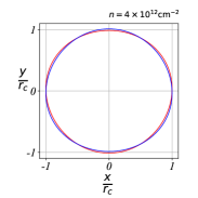
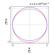
Valley separation: The effective Hamiltonian for graphene near the charge neutrality point is Dirac-like, , where are the usual Pauli matrices and reflect the two constituent sub-lattices. At low densities, there is a four-fold degeneracy, due to spin and valley degrees of freedom. The two inequivalent valleys are located at and respectively in the Brillouin zone, and close to the charge neutrality point are cylindrically symmetric. For higher densities, the Fermi surface in each valley and exhibits trigonal warping, the emergence of which is shown in Fig. 1.
With an applied transverse magnetic field, , where is the vector potential. If the applied field is weak, and the electron or hole density is high, the charge carrier dynamics can be described semi-classically, starting from the Heisenberg equation of motion for the operators,
| (1) |
where is the unit vector normal to the graphene plane, and is the magnitude of the applied magnetic field. Note that and are operators. Eq. (1) is general, and holds for a variety of dispersion relationsBladwell and Sushkov (2015). In the semiclassical limit, the operator equation, Eq. (1), is converted to a classical equation of the expectation values, which can then be trivially integrated to yield the real space motion of a electron under an applied transverse magnetic field,
| (2) |
where and . This is the equation of motion for cyclotron motion, with the electron following the equienergetiuc contours of the Fermi surface. Thus at high densities, the semi-classical cyclotron orbits of graphene are trigonally warped.


In Eq. (2), guiding centres of the two valleys are identically located at . This is shown in Fig. 2. For an electron optics device, for example, the pin-hole collimator designed in Ref. Barnard et al. (2017), the initial position of the wave packet is at , the location of the injector. In addition, for a perfectly collimated beam of electrons, the initial velocity is fully aligned along the axis, parallel to the channel of the injector. For a cylindrically symmetric Fermi surface, the location of the guiding centre co-ordinate is unchanged. When the Fermi contour becomes trigonally warped, the guiding centre co-ordinate becomes offset, proportional to the magnitude of the trigonal warping. This offset effect is presented in Fig. 2. Since the two valleys exhibit triagonal warping with opposite signs, the guiding centre co-ordinates are offset above and below the axis. The magnitude of the offset is proportional to the magnitude of the trigonal warping; as trigonal warping increases, so does guiding centre co-ordinate offset.
To illustrate the effect analytically, I consider the following approximation for the Fermi momentum, ,
| (3) |
where is the polar angle, , and . The valley index, , with , where is the lattice constant of graphene. It is important to note that this analytic approach is only valid while , that is, . The transverse velocity must vanish for collimated injection. From Eq. (2), the condition is , where . The guiding centre co-ordinate is
| (4) |
where is once again the valley index. This offset of the two valley states can be clearly seen in Fig. 2.
Right panel: Real space trajectories including the induced spacial offset from collimation, Eq. (4). The strong enhancement in the spatial offset between the two valley states make resolution of the individual valleys possible.
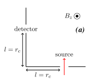
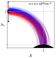
Focusing in the half plane, that is, with source and the detector located on the axis, does not yield any spatial separation between the valley states. However, if an orthogonal device setup is employed, as shown in Fig. 3a, the states can be spatial separated. The real space separation at the collector is
| (5) |
where and are the real space positions in the plane of the detector. Thus trigonal warping of the valleys in graphene induces a real space separation when combined with an appropriate device setup. The critical point to note is the significant enhancement; the required density for valley separation is reduced by a factor of 16, making it possible to resolve the individual valleys at experimentally achievable densities. This real space separation from collimated injection is shown in Fig. 3.
Resolution limits: On its own, Eq. (5) tells us little about whether the spatial splitting can be observed. If the broadening of the beam exceeds the spatial separation, then the valley states will overlap and resolution of the distinct valleys currents will not be possible. There are three specific sources of broadening that are relevant at cryogenic temperatures in high mobility samples; (1) the imperfect collimation of the source, (2) the spatial resolution of the detector, and (3), the beam broadening due to the medium and scattering.
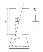
Top right panel: Pinhole collimator layout. The aperture width is , and the length , with the angular spread, given by the twice the projected angle. This is one possible collimating source in graphene, with current experimental devices producing a beam with a beam spread of .
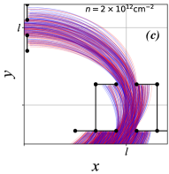
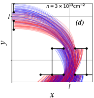
Lower panels: Trajectory computation for a pinhole collimator source, and pinhole aperture detector, with m, m, and . Trajectories are computed with a random initial condition (random guiding centre coordinate), with the transverse magnetic field, . Each valley has trajectories in red (blue). The parameters for the Pinhole collimator are chosen to be comparable to the device of Barnard et al Barnard et al. (2017). At very high density the separation between valleys can be seen. High density is required for the weak collimation of the pinhole collimator.
Firstly, we consider the resolution limits due to the imperfect collimation of the source. For a a pinhole style collimator setup in the orthogonal geometry of Fig. 3a, the allowed trajectories are those with guiding centre co-ordinates, , satisfying the limits, , . Here and represent the width and length of the pinhole collimator respectively, while is the focusing length. A schematic showing these is presented in Fig. 3b. Specifically, the value of interest is the range of , which must be less than the spatial separation of the valley states. Provided the trigonal warping is relatively small, , the radius of curvature in the local region about is identical for both valleys, and the trajectories within the collimator can be approximated by cyclotron orbits. The resulting approximate limit is , while the “spread” of the beam is double this. In the absence of any addition collimation, the required density for spatial separation for a pinhole collimator directly equivalent to that of Barnard et al is and is cm-2. Alternatively, the spread can be determined from typical values in the literature. For a pinhole collimator like that of Barnard et al, the angular full width half maximum was , corresponding to a spread of . For , , which yields a minimum density of cm-2. In general, the angular FWHM, scales as , thus the required density for the resolution of individual valleys scales as
| (6) |
Lithographic limits for feature sizes are typically nm.
Parabolic p-n junctions, as proposed by Liu et al have a significantly more collimated beam shape, with . Implementation using this type of beam gives , implying an electron density for resolution of the valleys of cm-2, well within the bounds of back-gated hexagonal Boron-Nitride devices. The limitation of this form of collimation is the larger beam expanse, . The corresponding spread of the beam at the detector is , which for focusing lengths of m is . Due to the quadratic scaling, the beam expanse becomes unimportant for larger . Combinations of parabolic junctions and pinhole aperture can further improve the angular distribution and spatial extent of the beamBøggild et al. (2017).
Next, we consider the resolution of the detector. By far the simplest setup is a pinhole aperture, with the voltage probe connected behind. For resolution of the individual valleys, the requirement is that the spatial separation of the valley peaks, , is greater than the width of the pinhole aperture, . For grounded contacts, the limitation on is lithography, nm. For a focusing length m, the ratio of the pinhole aperture to the focusing length can be . If both and , the required density for the resolution of individual valleys is cm-2, remarkably close to the densities of Barnard et al.
For such a device, a final question remains as to whether beam broadening due to the medium destroy resolution of the valley peaks. The path length of the ballistic measurements used in Ref. Barnard et al. (2017) were m, with negligible beam broadening. For an orthogonal device with a geometry equivalent to that of Fig. 3a, this corresponds to a maximum focusing length, m. Beam broadening due to scattering is therefore unimportant at cryogenic temperatures for m. In principle the device can be made significantly larger, the mean free path in h-BN encapsulated graphene can be upwards of m at densities cm-2Banszerus et al. (2016).
Numerical simulations: This can be grounded more firmly via numerical simulation of the device, to determine the required and therefore for resolution of the individual valleys. Since Eqs. (5) and (3) are valid only for small values of trigonal warping, I consider the energy bands of the usual tight-binding hamiltonian (see, for example, Neto et al. (2009)) to determine the equienergetic contours and then use Eq. (2) to determine the dynamics. As already noted, this approach is valid provided , and device feature sizes much large than the Fermi wavelength. We will consider both a pinhole collimator, equivalent to that shown in Fig. 3, and a parabolic p-n junction111See supplementary material [at url] for the python code used to generate the figures. Code comments provide details of the exact procedure..
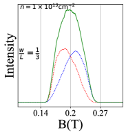
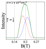
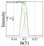
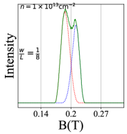
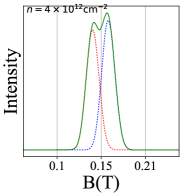
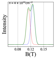
The results of the numerical procedure are presented in Figs. 4. For a device with a pinhole collimator, and a detector with a simple pinhole aperture equivalent to that of Barnard et al, the required density is greater than cm-2, as would be anticipated based on Eq. (6). With narrower apertures lowering the required density. At , the peaks can be clearly resolved at cm-2. This is well within current experimentally achievable densities for graphene devicesCraciun et al. (2011), however it requires specific gating techniques. Further improvements by reducing are possible. In principle there is a fundamental limit due to diffraction at low densities, however for cm-2, nm nm, and diffraction is essentially irrelevant.
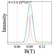
Next, we consider a parabolic PN junction for current injection, with the pinhole aperture for detection of the current. The considered parabolic PN junction is equivalent to that of Liu et al, with a gaussian beam width of nm, and a full width half maximum angular spread of Liu et al. (2017). We consider a pinhole aperture detector of width nm. The results of the numerical simulation are presented in Fig. 5. The valley split peaks can be resolved at cm-2, which is accessible in high mobility back gated devices. With an increased the focusing length, the resolution improves, due to the increase in the real space separation of the valley states. Finally, we note that the relative valley warping at cm-2 is extremely small, . That individual valley states can be resolved is an illustration of the significant enhancement present in Eq. (5). It is this enhancement that makes the valley separation possible.
Top right panel: Focusing spectrum for the parabolic PN junction, with m, nm, cm-2.
Lower left panel: Focusing spectrum for the parabolic PN junction, with m, nm, cm-2.
Lower right panel: Focusing spectrum for the parabolic PN junction, with m, nm, cm-2. Increasing the focusing length increases the separation of the valley states, and thereby improves resolution.
In conclusion, we have shown that the ballistic trajectories of electrons in different valleys of graphene can be spatial separated using a collimating source, and a weak magnetic field. With an appropriately chosen geometry, the offset in different valleys due to trigonal warping is strongly enhanced. The magnitude of the valley separation at cm-2 is sufficient to fully resolve the individual peaks when the source is a parabolic PN junction, and this carrier density is achievable with current gating methods, in high mobility back gated devices. For pinhole collimators, resolution is lower, due to the greater spread of the beam, and the density requirements for experimentally feasible devices are therefore larger. Finally, the basic principle of valley separation outlined here will work for any two dimensional systems where the valleys exhibit trigonal warping, including bilayer graphene, moire superlattices, and two dimensional transitional metal dichalcogenides, and all will exhibit this enhancement. This research was partially supported by the Australian Research Council Centre of Excellence in Future Low-Energy Electronics Technologies (project number CE170100039) and funded by the Australian Government. SSRB would like to thank Oleg Sushkov for his critical reading and suggestions.
References
- Rycerz et al. (2007) A. Rycerz, J. Tworzydło, and C. Beenakker, Nature Physics 3, 172 (2007).
- Schaibley et al. (2016) J. R. Schaibley, H. Yu, G. Clark, P. Rivera, J. S. Ross, K. L. Seyler, W. Yao, and X. Xu, Nature Reviews Materials 1, 16055 (2016).
- Garcia-Pomar et al. (2008) J. Garcia-Pomar, A. Cortijo, and M. Nieto-Vesperinas, Physical review letters 100, 236801 (2008).
- Gunlycke and White (2011) D. Gunlycke and C. T. White, Physical Review Letters 106, 136806 (2011).
- Jiang et al. (2013) Y. Jiang, T. Low, K. Chang, M. I. Katsnelson, and F. Guinea, Physical review letters 110, 046601 (2013).
- Settnes et al. (2016) M. Settnes, S. R. Power, M. Brandbyge, and A.-P. Jauho, Physical review letters 117, 276801 (2016).
- Akhmerov and Beenakker (2007) A. Akhmerov and C. Beenakker, Physical review letters 98, 157003 (2007).
- Golub et al. (2011) L. E. Golub, S. A. Tarasenko, M. V. Entin, and L. I. Magarill, Physical Review B 84 (2011).
- Wehling et al. (2015) T. Wehling, A. Huber, A. Lichtenstein, and M. Katsnelson, Physical Review B 91, 041404 (2015).
- Banszerus et al. (2016) L. Banszerus, M. Schmitz, S. Engels, M. Goldsche, K. Watanabe, T. Taniguchi, B. Beschoten, and C. Stampfer, Nano letters 16, 1387 (2016).
- Barnard et al. (2017) A. W. Barnard, A. Hughes, A. L. Sharpe, K. Watanabe, T. Taniguchi, and D. Goldhaber-Gordon, Nature communications 8, 15418 (2017).
- Liu et al. (2017) M.-H. Liu, C. Gorini, K. Richter, et al., Physical review letters 118, 066801 (2017).
- Bladwell and Sushkov (2015) S. Bladwell and O. Sushkov, Physical Review B 92 (2015).
- Bøggild et al. (2017) P. Bøggild, J. M. Caridad, C. Stampfer, G. Calogero, N. R. Papior, and M. Brandbyge, Nature communications 8, 15783 (2017).
- Neto et al. (2009) A. C. Neto, F. Guinea, N. M. Peres, K. S. Novoselov, and A. K. Geim, Reviews of modern physics 81, 109 (2009).
- Craciun et al. (2011) M. F. Craciun, S. Russo, M. Yamamoto, and S. Tarucha, Nano Today 6, 42 (2011).