Deep learning meets nanophotonics: A generalized accurate predictor for near fields and far fields of arbitrary 3D nanostructures
Abstract
Deep artificial neural networks are powerful tools with many possible applications in nanophotonics. Here, we demonstrate how a deep neural network can be used as a fast, general purpose predictor of the full near-field and far-field response of plasmonic and dielectric nanostructures. A trained neural network is shown to infer the internal fields of arbitrary three-dimensional nanostructures many orders of magnitude faster compared to conventional numerical simulations. Secondary physical quantities are derived from the deep learning predictions and faithfully reproduce a wide variety of physical effects without requiring specific training. We discuss the strengths and limitations of the neural network approach using a number of model studies of single particles and their near-field interactions. Our approach paves the way for fast, yet universal methods for design and analysis of nanophotonic systems.
keywords: deep learning, nano-photonics, rapid nano-optics simulations, silicon nanostructures, plasmonics
Dielectric and metallic nanostructures of sub-wavelength size can be designed such that their interaction with light differs significantly from bulk materials. Nanophotonics aims to exploit optical resonances and strong localized fields that can be designed by nanoparticle geometry and material choices.Draine and Flatau (1994); Evlyukhin et al. (2011); Kinkhabwala et al. (2009); Albella et al. (2013) The unique nanoscale properties can be used in applications such as plasmonic nanoantennas for near-field energy concentration and meta-surfaces for directing and controlling light. More complex optical behavior can be designed such as polarization conversion,Wiecha et al. (2017) chirality, Schäferling et al. (2012) localized heat generation Baffou et al. (2010) or nonlinear optical effects Kauranen and Zayats (2012); Shcherbakov et al. (2014); Wiecha et al. (2016).
The interaction of light with many types of nanostructures can be modelled accurately by solving the classical Maxwell’s equations,Maxwell (1865) for which many commercial and open source methods are available. However, numerical nanophotonic simulations are often time-consuming and can take hours or even days for complex systems.Smajic et al. (2009) Many subsequent simulations are needed for iterative optimization methods such as the rational design of nanosystems by topology optimization and inverse design.Liu et al. (2018); Feichtner et al. (2012); Wiecha et al. (2017); Kingston et al. (2019) Fast evaluation of optical properties is highly desirable also for example in real-time sensors based on 3D molecular nanorulers, Liu et al. (2011); Kuzyk et al. (2014) or in the active control of smart and reconfigurable nano-materials Zhou et al. (2017); Qian and Ginger (2017).
Methods of artificial intelligence, and in particular deep learning,Goodfellow et al. (2016); LeCun et al. (2015) are powerful tools with potentially groundbreaking relevance for nano-optics. First captivating applications have been reported in experimental photonics and nano-optics. Examples are the possibility of phase recovery in conventional microscopy,Rivenson et al. (2017) stabilization of lasersBaumeister et al. (2018) and a large variety of applications in data analysis and interpretationCirovic (1997); Ciresan et al. (2012); Wang et al. (2014); Ziatdinov et al. (2017); Jo et al. (2017); Zhang et al. (2018); Han et al. (2019); Wiecha et al. (2019); Timoshenko et al. (2019). For forward modelling, early work has shown that artificial neural networks (ANNs) can be used as approximate predictors for light-matter interaction phenomena or optical scattering at nanostructures. Examples are strong-field ionization of potassium atoms,Selle et al. (2008) SHG of a specific fluorescent molecule,Selle et al. (2007) the optical transmittance of “H”-shaped particlesMalkiel et al. (2018) or the scattering cross sections of multilayer spheresPeurifoy et al. (2018). All of those reported ANN techniques apply to single, very specific problems and for a particular nanostructure geometry.
Furthermore, deep artificial neural networks are highly promising to approach notoriously difficult inverse problems in nano-optics, like the design of meta-surfaces or the tailoring of optical properties of individual nano-structures. Even though no generalized and fast inverse design method has as yet been reported, rapid progress has been made in this direction over the last two years.Malkiel et al. (2018); Peurifoy et al. (2018); Liu et al. (2018, 2018, 2019); An et al. (2019); Chen et al. (2019); Liu et al. (2019); Jiang and Fan (2019) The overall trend in these studies so far is, that for every specific inverse problem using a particular geometric model, a neural network needs to be designed in a time demanding and computationally very expensive process, involving hyper-parameter optimization, training data generation, training and extensive testing.
Here, we present a general approach to nano-optical modeling which is distinct from all previous works by its capability for fast and accurate modeling of generalized nano-optical effects in a variety of nanostructures. Requiring only a single training procedure, our concept fully generalizes ANNs for nano-photonic simulations and allows to tremendously accelerate predictions for countless problems in nano-optics. We demonstrate that the generalized network captures a range of complex nano-optical near- and far-field effects in nanostructures, such as higher order antenna resonances, electric and magnetic dipole modes, non-radiating anapole states or Kerker-type directional scattering, without the need of any specific training for these effects. Our approach is based on a three-dimensional, fully convolutional neural network (CNN), trained on predicting a coupled dipole representation of the fields inside nanostructures of arbitrary shape. These predictions can be used subsequently to reconstruct many secondary physical quantities with uncertainties as low as few percent.
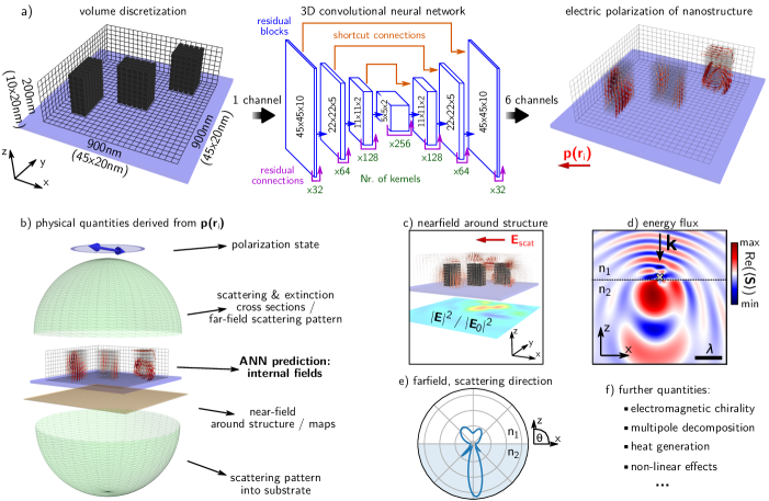
An overview of the model description is shown in Figure 1. The aim of our work is to develop an ANN capable of predicting the time-harmonic electric polarization density inside nanostructures of arbitrary shape. For our demonstration we use a geometric model consisting of a rectangular grid of positions, as illustrated by the example of Figure 1a, left panel. Nanostructures are mapped onto the 3D grid using a standard volume discretization approach. The resulting geometry can be directly evaluated with numerical simulations using the coupled dipole approximation (CDA). Upon normal incidence plane wave illumination ( along ) and linear polarization along , we numerically calculate the field at every mesh cell inside the nanostructure via the Green Dyadic Method (GDM),Girard (2005) for which we use a home-built python implementation “pyGDM”.Wiecha (2018) A short summary of the GDM formalism can be found in Section I of the Supporting Information. The model includes a dielectric substrate (). While in principle any simulation method can be used to generate the network training data, we use the GDM for its simplicity and its good convergence in the case of small nanostructures as well as for the fact that the results are by design available on the required cubic discretization grid.
The conceptual beauty of the CDA method lies in the initial assumption that every meshpoint can be approximated by a dipolar polarizability, which allows to treat every cell inside the nanostructure as an oscillating dipole moment. In consequence, various physical quantities in the near-field as well as in the far-field region can be derived from the internal fields of a CDA simulation. Figure 1b illustrates a few of the possible observables that can be calculated from the dipole discretization. Using according Green’s dyads, the optical electric and magnetic fields (and in consequence the Poynting vector) can be obtained at any location outside the nanostructure (see Figure 1(c-d)).Wiecha (2018) Extinction, scattering or absorption cross sections can be calculated almost effortless,Draine and Flatau (1994) as well as the polarization state and spatial patterns of the scattering (Figure 1e),Wiecha et al. (2017, 2017) the dissipated heat or local temperature gradients,Baffou et al. (2010); Girard et al. (2018) nonlinear effects like second or third harmonic generation and multi-photon luminescenceWiecha et al. (2016); Balla et al. (2010); Teulle et al. (2012) or the multipole decomposition of the optical response.Evlyukhin et al. (2011) In consequence, an ANN capable to accurately predict the internal electric fields of a photonic nanostructure represents a generalized, phenomenological model of light-matter interaction, with tremendous potentials for rapid nano-optical simulations.
A 3D grid of positions is used as input layer to the network which is illustrated in Figure 1a, middle panel. The network used in this study is a three-dimensional symmetric, fully convolutional network with “U-Net”-type shortcut connections between corresponding convolutional and up-sampling units. This type of ANN is known to be particularly strong at the reconstruction of spatial information.Ronneberger et al. (2015) Shortcuts were found to be essential for our purpose to obtain good approximations of the internal fields. In addition to the U-Net design, we organize the network in residual blocks He et al. (2015); Szegedy et al. (2016) which allows us to maintain good learning performance on a very deep architecture with as much as 91 layers including 33 three-dimensional convolutional operations. All network details and hyperparameters are given in Section III of the Supporting Information.
The output of the network is composed of layers of the same size as the input grid, which correspond to the real and imaginary parts of , and . We use complex amplitudes for the fields, so phase information and retardation effects are included in the neural network predictions. An illustration of real part field-vectors is shown in Figure 1a, right panel.
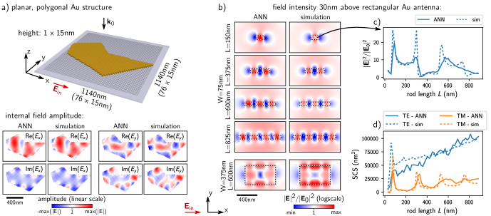
For the network training, we simulate the internal fields of 30000 random nanostructures. We test the network on two datasets, the first contains planar gold nanostructures (nm height) of random polygonal shapes. The second set is composed of silicon pillar structures (nm height), consisting of one or more arranged cuboidal blocks. Details about the geometric models are given in Section II of the Supporting Information. For convenience we use fixed height structures throughout this demonstration, but we want to emphasize that this is not an inherent limitation of the approach. On the contrary, variable height structures can be modeled without any further modifications and without significant loss of accuracy, as shown in the supporting information figure S9. We fix the illumination conditions to normal incidence plane wave excitation at a wavelength of nm with linear polarization along . In consequence, the neural network is limited to predictions under the conditions chosen for the training data generation. Hence, in our approach a separate ANN needs to be trained if the structure model or material is modified and also for every illumination configuration, e.g. for every angle of an oblique incidence illumination. We note that under normal incidence, any linear polarization angle can be achieved by a rotation of the nanostructure. Fully arbitrary polarization states of the illumination can furthermore be obtained via superposition of perpendicular linear polarizations, as demonstrated in the supporting information Fig. S7 for left circular polarization.
In both cases of plasmonic and dielectric structures we use 28000 samples for training and the remaining 2000 structures for validation and benchmarking. On an NVIDIA P6000 GPU, the training with the gold (silicon) dataset takes around 2 (10) minutes per epoch. We stop training after 100 epochs, longer training leads to no further improvement in validation accuracy (see Figure S10 in the Supporting Information). On the same GPU, the trained network delivers its prediction in around ms for a planar gold structure and ms for a silicon structure. On a third generation Intel i7 quad-core CPU (i7-3770) the predictions for the gold, respectively silicon structures take around ms and ms. Depending on the chosen hardware platform, this is to orders of magnitude faster than the conventional simulations, which take seconds to minutes on the Intel i7 CPU. The simulation time for the full datasets, running in parallel on two workstations, was approximately days. We note that since the simulations are entirely independent, the data generation is a so-called “embarrassingly parallel” task that can be parallelized to any extent. The GDM simulations can potentially be accelerated by GPUs, but according to literature, less than one order of magnitude speed-up is expected for GPU-based LU decomposition.Ozcan and Sen (2012)
While a more formal benchmarking of the ANN is discussed further below, we start our results by demonstrating the ability of the network to capture some of the well-known physical effects in metallic and dielectric nanostructures. The ANN’s capability to generalize to these arbitrary situations is tested by constructing a number of specific cases at which optical effects occur and compare the predictions of the neural network to numerical simulations. Figure 2a shows the ANN predicted real and imaginary part of the amplitude of the internal field components and upon polarized plane wave illumination of the planar gold nano-polygon.Viarbitskaya et al. (2013); Frank et al. (2017) Clearly, the neural network correctly predicts the form and distribution of fields as given by the CDA simulation. In addition to arbitrary objects, the ANN shows a good systematic scaling of antenna behaviour, as illustrated in Figure 2b where we plot the magnitude of the electric field intensity for gold nanorod antennas of nm width and lengths ranging from a point dipole, to half-wave and multi-order antenna resonances. In figure 2c, the electric field intensity on top of the center of the nanorod is shown as function of the rod length. The neural network is able to make an accurate prediction of the mode structure and effective scaling of plasmonic nanoantennas within the domain under study in a generalized, phenomenological model of light-matter interaction.Novotny (2007) We note that the peak field enhancement at resonance is consistently underestimated by the ANN. We believe this is due to the random generation process of the training data, which therefore includes only very few structures that exactly hit a resonance condition.
In Figure 2d we finally show the scattering cross section (SCS) of a gold rod antenna as function of its length for perpendicular incident polarizations TE (incident field polarized perpendicular to the rod long axis) and TM (field along the rod axis). Again the neural network reliably predicts the resonance positions. Interestingly, apart from the dipole antenna resonance where the underestimated nearfield is reflected also in the SCS, prediction and scattering quantitatively matches better for longer rod antennas. This is a result of the weak coupling to the far-field of higher order modes, hence the underestimation of the nearfield strength has no great impact on the far-field scattering in these cases.
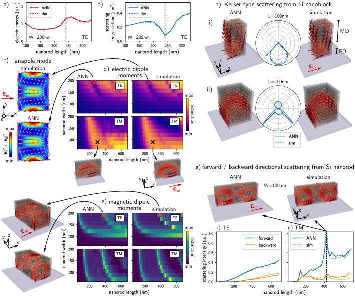
Next to plasmonic nanoparticles and antennas, recently dielectric nanostructures have received tremendous interest for use in meta-surfaces and low-absorption antennas.Kuznetsov et al. (2016); Barreda et al. (2019) Here, we evaluate the performance of the ANN in inferring the response of silicon nanorods with fixed height of 200 nm and varying lengths and widths. Figure 3a and b shows the internal electric field energy (a) and scattering cross section (b) for a silicon nanorod with a square cross-section of nm2, plotted against rod length. The incident plane wave is linearly polarized along the width of the rod (transverse electric, TE). In this dataset we observe the typical signature of an “anapole” mode for a length indicated by a dashed vertical line, at which a superposition of toroidal and electric dipole mode is excited.Miroshnichenko et al. (2015) The anapole mode is characterized by a minimum in the scattering cross section accompanied by a maximum of the electric field energy inside the structure.Grinblat et al. (2016) Both signatures are reproduced by the ANN (solid lines) in excellent agreement with the numerical simulations (dashed lines). The corresponding field profile predicted by the ANN is shown in Figure 3c and reproduces the characteristic internal field distribution of the anapole.
The response of the silicon nanorods for polarizations along the width (TE) and along the length (TM) of the nanorod is further investigated in a parameter study where we independently tuned the length and width of the structure. Figure 3d and 3e show the electric and magnetic dipole contributions to the nanorod extinctions. The two separate contributions were extracted from the total solution through a Taylor-like expansion of the electric polarization.Evlyukhin et al. (2011) The neural network predictions (left subplots) agree very well with the numerical simulations (right subplots) in both the positions and amplitudes of the different magneto-electric modes in the structure. Also shown are 3D quiver plots of the internal field distributions at selected parameters, which show that the underlying field distributions inferred by the network match very well the simulated ones.
Precise tuning of the nanostructure geometry allows to obtain specific conditions of uni-directional “Kerker-type” light scattering due to the simultaneous excitation of electric dipole (ED) and magnetic dipole (MD) modes of similar magnitude.Staude et al. (2013); Wiecha et al. (2017); Shibanuma et al. (2016) For the fixed structure height of 200 nm and illumination wavelength used in our predictor network ( nm), we find that ED and MD modes are simultaneously excited for a square cuboid with side length nm. Figure 3f shows a 3D quiver plot (i) where the MD can be observed in the upper part of the 3D electric field distribution (vortex formed by the field vectors), whereas the ED is situated at the bottom of the silicon block (field vectors parallel to the substrate plane). The superposition of both contributions leads to a strongly directional scattering pattern (see center plot). Panel (ii) shows the effect when the block size is increased to nm. Here the MD becomes the predominantly excited mode, leading to a bi-directional scattering, as expected for a dipolar source of radiation. Both internal 3D field plots as well as the far-field scattering patterns show very good agreement between ANN and simulation. Generally the ratio of forward to backward total scattering is of interest in dielectric structures as it shows large variations with particle geometry. Figure 3g shows the forward / backward ratio for a silicon nanorod of nm width and with increasing length for (i) TE and (ii) TM polarized illumination. The scattering from the nanorods was integrated over the respective full half hemisphere to obtain the total scattering intensity. Overall, the ANN predicts accurately the directional character of the scattering in all cases. The position of the quadrupole magnetic mode is indicated by the vertical line, even the quite complex electric field distributions at this position are correctly predicted by the network. For longer rods (nm), the accuracy of the ANN deteriorates slightly, the network tends to overestimate scattering and extinction cross sections (see Figure 3(d-e) and 3g). We assume that this is due to the maximum length and width of nm used for the silicon blocks in the training data. Considering this constraint on the training process, the network manages to generalize impressively well to larger individual nanostructures. In summary, our generalized predictor neural network manages to accurately predict various nano-optical phenomena in the near-field as well as in the far-field, without having been specifically trained on those effects.
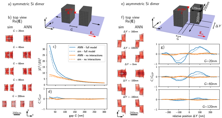
Next to the response of individual structures, it is critically important that the ANN can capture the mutual interactions between isolated nanostructures. Figure 4 explores the near-field coupling for a silicon dimer structure. Results for gold nanodimers are shown in the Supporting Information Figure S6. The scaling of near-field coupling between the structures was studied by varying the inter-particle gap as illustrated in Figure 4a. The effect of near-field coupling is clearly visible in the quiver plots in Figure 4b. Visually the network predictions can barely be distinguished from the numerical simulations. Quantitative agreement is also obtained for the scaling of the near-field in the center of the gap (indicated by a red cross in Figure 4a). The field enhancement derived via ANN is compared in Figure 4c (solid lines) to numerical simulations (dashed lines), yielding indeed an excellent agreement, apart from a slight overestimation of the field intensity.
In order to assess the impact of optical coupling between the two silicon blocks, we artificially turn off near-field interactions in the simulations (orange lines). This is done by calculating the optical response of both blocks separately, and using the internal dipole moments of those isolated simulations (respectively isolated ANN predictions) to derive the field intensity in the gap. We find that near-field interactions become non-negligible only for small distances nm, which is correctly described also by the predictor network. This observation is in agreement with experimental results of cathodoluminescence imaging of hybridized mode field profiles in silicon dimers.van de Groep et al. (2016)
In figure 4d, we furthermore study the optical chirality of the near-field in the center of the gap, nm above the nanostructure’s top surface. is a measure of the selectivity at which opposite handed chiral molecules interact with the electromagnetic field.Tang and Cohen (2010); Meinzer et al. (2013) We plot normalized to the chirality of a left circular polarized plane wave . As expected, in the symmetric configuration the field has no chirality. It is however possible to break the symmetry of the dimer by shifting one of the blocks vertically by a distance , as illustrated in Figure 4e. The internal fields are shown in top-view quiver plots in Figure 4f and provide evidence that the neural network correctly predicts near-field coupling effects in the asymmetric dimer. The electric field vectors inside the silicon strongly vary dependent on the relative positions of the two blocks. The optical chirality as function of the vertical shift is shown in Figure 4g for three different gap sizes. Chirality is induced through asymmetry in the dimer geometry, which is again correctly reflected in the ANN predictions. Interestingly, the electromagnetic field above the gap features almost no chirality if the near-field interactions are deactivated in the simulations. Hence, the electromagnetic chirality is driven here by optical coupling between the two silicon blocks. This is confirmed by the decreasing magnitude of for increasing gap widths (from top to bottom in Figure 4g), which is also in agreement with recent experimental results.Zhao and Reinhard (2019) In contrast, for plasmonic dimers, it is found that near-field coupling suppresses the chirality (Supporting Information Figure S6).Meinzer et al. (2013)
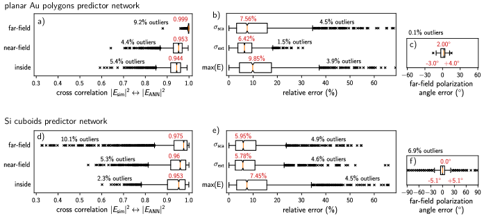
The above results reveal the capacity of the neural network in inferring many of the important physical effects in the interaction of light with nanostructures. While the simple model examples provide insight, a more formal assessment of the ANN performance is needed. Figure 5 shows results of the statistical data analysis of the entire validation set for the plasmonic (a-c) and silicon (d-f) models, each consisting of 2000 random structures which were not used for training. In Figure 5a and d the statistics for the normalized cross correlation between simulated and predicted field intensity distributions are shown for the far-field, the near-field in the vicinity, and the internal field inside the structure. Considering that a cross correlation of 0.8 indicates already a good qualitative agreement, the network predictions are mostly excellent, however for a non-negligible number of “outliers”, the ANN results are significantly worse.
The same trends can be found in a quantitative analysis of the far-field cross-sections, the peak internal field intensity (Figure 5b,e) and the polarization state (Figure 5c,f). So while the network predictions are mostly very good, being a data-driven approach, an inevitable error of a few percent is inherent to the method. Also, the ANN bears some risk of getting a result with significant error. The risk of a failed prediction is of the order of around , as expressed by the amount of outliers in figure 5. Examples of outliers in the validation data are shown in Figure S4 and S5 of the Supporting Information. In our simple examples we have also seen some reduction in ANN performance around resonant poles in the polarizability and for larger sized structures in Figure 2. The statistical evaluation indicates that the plasmonic predictor network performs generally worse than the ANN trained on silicon cuboidal structures. The induced plasmonic currents cause strong depolarization effects on short length-scales, which are strongly dependent on the structure geometry. We therefore speculate that this complex and feature-rich plasmonic optical response is more difficult to predict, compared to dielectric nanostructures. This lack of perfection is the general property of neural networks and new methods gauging the reliability of solutions have been proposed using for example multiple, independently trained ANNs.Wang et al. (2019) Additionally, while ANNs are good at interpolating complex functions from few data, their performance is reduced when extrapolating outside of the known parameter space.Nadell et al. (2019) Despite these limitations, our results clearly show that the ANN’s capabilities go far beyond that of a simple fit function, as it is able to apply trained behavior to new highly nontrivial configurations (see also Supporting Information Figure S8 on the prediction of curved structures). The ANN yields a generalized and powerful capability for generating field distributions from structural arrangements.
Improved performance of the ANN in specific ranges may be achieved by further extending the training dataset. In our current demonstration we chose to limit ourselves to planar configurations and single materials. However the method could be further generalized to arbitrary hybrid-material structures using the three-dimensional distribution of the dielectric constant as input. Periodic structures can be treated using training data describing one unit-cell of the periodic structure.Gallinet and Martin (2009); Evlyukhin et al. (2010) In addition, the approach can be extended to spectrally resolved predictions using multiple output layers. Spectral training might be accelerated by transfer learning. Generalized predictor networks can be potentially used together with evolutionary optimization schemes for fast, universal nano-photonic inverse design, overcoming the need of designing a specific inverse network for every target problem and nanostructure model.Hegde (2020)
In conclusion, we presented an approach combining the coupled dipole approximation with deep artificial neural networks, which is capable to accelerate universal electro-dynamical simulations of arbitrary 3D nanostructures by many orders of magnitude. Our generalized predictor network needs to be trained only once using a volume discretization of the three-dimensional electric polarization inside nanostructures of arbitrary shape. Being a data-driven approach, the method comes necessarily with a loss of accuracy. Despite this inherent shortcoming, we could demonstrate that the network predictions imply only a small error in the order of around five percent. On the other hand, the prediction of the internal fields allows to derive manifold quantities and effects in the near-field as well as in the far-field region. We have shown, that both regions are covered by the predictor with very good accuracy. We demonstrated furthermore that the network developed a generalized intuition about Maxwell’s equations, being capable to reproduce complex nano-optical effects occurring in plasmonic and dielectric nanostructures. The ANN faithfully reproduces phenomena like higher order localized plasmon modes, magnetic and electric dipole modes, non-radiating anapole states, Kerker-type directional scattering or optical chirality. We demonstrated that the network also developed an understanding of near-field interactions between separated nanostructures. We foresee that ultra-rapid generalized predictor networks bare tremendous potential for applications in nanophotonics.
Acknowledgements.
We gratefully thank Arnaud Arbouet and Christian Girard for fruitful discussions. We thank the NVIDIA Corporation for the donation of a Quadro P6000 GPU used for this research. This work was supported by the German Research Foundation (DFG) through a research fellowship (WI 5261/1-1). OM acknowledges support through EPSRC grant EP/M009122/1. All data supporting this study are openly available from the University of Southampton repository (DOI: 10.5258/SOTON/D1088).Supporting Informations
A description of methods and further data with Figures S1-S10. A video of the oscillating fields inside the silicon nano-dimer for varying vertical distances comparing ANN and simulation. This material is available free of charge via the Internet at http://pubs.acs.org.
References
- Draine and Flatau (1994) Draine, B. T.; Flatau, P. J. Discrete-Dipole Approximation for Scattering Calculations. Journal of the Optical Society of America A 1994, 11, 1491.
- Evlyukhin et al. (2011) Evlyukhin, A. B.; Reinhardt, C.; Chichkov, B. N. Multipole Light Scattering by Nonspherical Nanoparticles in the Discrete Dipole Approximation. Physical Review B 2011, 84, 235429.
- Kinkhabwala et al. (2009) Kinkhabwala, A.; Yu, Z.; Fan, S.; Avlasevich, Y.; Müllen, K.; Moerner, W. E. Large Single-Molecule Fluorescence Enhancements Produced by a Bowtie Nanoantenna. Nature Photonics 2009, 3, 654–657.
- Albella et al. (2013) Albella, P.; Poyli, M. A.; Schmidt, M. K.; Maier, S. A.; Moreno, F.; Sáenz, J. J.; Aizpurua, J. Low-Loss Electric and Magnetic Field-Enhanced Spectroscopy with Subwavelength Silicon Dimers. The Journal of Physical Chemistry C 2013, 117, 13573–13584.
- Wiecha et al. (2017) Wiecha, P. R.; Black, L.-J.; Wang, Y.; Paillard, V.; Girard, C.; Muskens, O. L.; Arbouet, A. Polarization Conversion in Plasmonic Nanoantennas for Metasurfaces Using Structural Asymmetry and Mode Hybridization. Scientific Reports 2017, 7, 40906.
- Schäferling et al. (2012) Schäferling, M.; Dregely, D.; Hentschel, M.; Giessen, H. Tailoring Enhanced Optical Chirality: Design Principles for Chiral Plasmonic Nanostructures. Physical Review X 2012, 2, 031010.
- Baffou et al. (2010) Baffou, G.; Quidant, R.; Girard, C. Thermoplasmonics Modeling: A Green’s Function Approach. Physical Review B 2010, 82, 165424.
- Kauranen and Zayats (2012) Kauranen, M.; Zayats, A. V. Nonlinear Plasmonics. Nature Photonics 2012, 6, 737–748.
- Shcherbakov et al. (2014) Shcherbakov, M. R.; Neshev, D. N.; Hopkins, B.; Shorokhov, A. S.; Staude, I.; Melik-Gaykazyan, E. V.; Decker, M.; Ezhov, A. A.; Miroshnichenko, A. E.; Brener, I.; Fedyanin, A. A.; Kivshar, Y. S. Enhanced Third-Harmonic Generation in Silicon Nanoparticles Driven by Magnetic Response. Nano Letters 2014, 14, 6488–6492.
- Wiecha et al. (2016) Wiecha, P. R.; Arbouet, A.; Girard, C.; Baron, T.; Paillard, V. Origin of Second-Harmonic Generation from Individual Silicon Nanowires. Physical Review B 2016, 93, 125421.
- Maxwell (1865) Maxwell, J. C. A Dynamical Theory of the Electromagnetic Field. Philosophical Transactions of the Royal Society of London 1865, 155, 459–512.
- Smajic et al. (2009) Smajic, J.; Hafner, C.; Raguin, L.; Tavzarashvili, K.; Mishrikey, M. Comparison of Numerical Methods for the Analysis of Plasmonic Structures. Journal of Computational and Theoretical Nanoscience 2009, 6, 763–774.
- Liu et al. (2018) Liu, D.; Tan, Y.; Khoram, E.; Yu, Z. Training Deep Neural Networks for the Inverse Design of Nanophotonic Structures. ACS Photonics 2018, 5, 1365–1369.
- Feichtner et al. (2012) Feichtner, T.; Selig, O.; Kiunke, M.; Hecht, B. Evolutionary Optimization of Optical Antennas. Physical Review Letters 2012, 109, 127701.
- Wiecha et al. (2017) Wiecha, P. R.; Arbouet, A.; Girard, C.; Lecestre, A.; Larrieu, G.; Paillard, V. Evolutionary Multi-Objective Optimization of Colour Pixels Based on Dielectric Nanoantennas. Nature Nanotechnology 2017, 12, 163–169.
- Kingston et al. (2019) Kingston, B. R.; Syed, A. M.; Ngai, J.; Sindhwani, S.; Chan, W. C. W. Assessing Micrometastases as a Target for Nanoparticles Using 3D Microscopy and Machine Learning. Proceedings of the National Academy of Sciences 2019, 201907646.
- Liu et al. (2011) Liu, N.; Hentschel, M.; Weiss, T.; Alivisatos, A. P.; Giessen, H. Three-Dimensional Plasmon Rulers. Science 2011, 332, 1407–1410.
- Kuzyk et al. (2014) Kuzyk, A.; Schreiber, R.; Zhang, H.; Govorov, A. O.; Liedl, T.; Liu, N. Reconfigurable 3D Plasmonic Metamolecules. Nature Materials 2014, 13, 862–866.
- Zhou et al. (2017) Zhou, C.; Duan, X.; Liu, N. DNA-Nanotechnology-Enabled Chiral Plasmonics: From Static to Dynamic. Accounts of Chemical Research 2017, 50, 2906–2914.
- Qian and Ginger (2017) Qian, Z.; Ginger, D. S. Reversibly Reconfigurable Colloidal Plasmonic Nanomaterials. Journal of the American Chemical Society 2017, 139, 5266–5276.
- Goodfellow et al. (2016) Goodfellow, I.; Bengio, Y.; Courville, A. Deep Learning; MIT Press, 2016.
- LeCun et al. (2015) LeCun, Y.; Bengio, Y.; Hinton, G. Deep Learning. Nature 2015, 521, 436–444.
- Rivenson et al. (2017) Rivenson, Y.; Zhang, Y.; Gunaydin, H.; Teng, D.; Ozcan, A. Phase Recovery and Holographic Image Reconstruction Using Deep Learning in Neural Networks. arXiv:1705.04286 [physics] 2017,
- Baumeister et al. (2018) Baumeister, T.; Brunton, S. L.; Kutz, J. N. Deep Learning and Model Predictive Control for Self-Tuning Mode-Locked Lasers. JOSA B 2018, 35, 617–626.
- Cirovic (1997) Cirovic, D. A. Feed-Forward Artificial Neural Networks: Applications to Spectroscopy. TrAC Trends in Analytical Chemistry 1997, 16, 148–155.
- Ciresan et al. (2012) Ciresan, D.; Giusti, A.; Gambardella, L. M.; Schmidhuber, J. In Advances in Neural Information Processing Systems 25; Pereira, F., Burges, C. J. C., Bottou, L., Weinberger, K. Q., Eds.; Curran Associates, Inc., 2012; pp 2843–2851.
- Wang et al. (2014) Wang, B.; Cancilla, J. C.; Torrecilla, J. S.; Haick, H. Artificial Sensing Intelligence with Silicon Nanowires for Ultraselective Detection in the Gas Phase. Nano Letters 2014, 14, 933–938.
- Ziatdinov et al. (2017) Ziatdinov, M.; Dyck, O.; Maksov, A.; Li, X.; Sang, X.; Xiao, K.; Unocic, R. R.; Vasudevan, R.; Jesse, S.; Kalinin, S. V. Deep Learning of Atomically Resolved Scanning Transmission Electron Microscopy Images: Chemical Identification and Tracking Local Transformations. ACS Nano 2017, 11, 12742–12752.
- Jo et al. (2017) Jo, Y.; Park, S.; Jung, J.; Yoon, J.; Joo, H.; Kim, M.-h.; Kang, S.-J.; Choi, M. C.; Lee, S. Y.; Park, Y. Holographic Deep Learning for Rapid Optical Screening of Anthrax Spores. Science Advances 2017, 3, e1700606.
- Zhang et al. (2018) Zhang, P.; Liu, S.; Chaurasia, A.; Ma, D.; Mlodzianoski, M. J.; Culurciello, E.; Huang, F. Analyzing Complex Single-Molecule Emission Patterns with Deep Learning. Nature Methods 2018, 15, 913.
- Han et al. (2019) Han, B. et al. Deep Learning Enabled Fast Optical Characterization of Two-Dimensional Materials. arXiv:1906.11220 [cond-mat, physics:physics] 2019,
- Wiecha et al. (2019) Wiecha, P. R.; Lecestre, A.; Mallet, N.; Larrieu, G. Pushing the Limits of Optical Information Storage Using Deep Learning. Nature Nanotechnology 2019, 1.
- Timoshenko et al. (2019) Timoshenko, J.; Wrasman, C. J.; Luneau, M.; Shirman, T.; Cargnello, M.; Bare, S. R.; Aizenberg, J.; Friend, C. M.; Frenkel, A. I. Probing Atomic Distributions in Mono- and Bimetallic Nanoparticles by Supervised Machine Learning. Nano Letters 2019, 19, 520–529.
- Selle et al. (2008) Selle, R.; Brixner, T.; Bayer, T.; Wollenhaupt, M.; Baumert, T. Modelling of Ultrafast Coherent Strong-Field Dynamics in Potassium with Neural Networks. Journal of Physics B: Atomic, Molecular and Optical Physics 2008, 41, 074019.
- Selle et al. (2007) Selle, R.; Vogt, G.; Brixner, T.; Gerber, G.; Metzler, R.; Kinzel, W. Modeling of Light-Matter Interactions with Neural Networks. Physical Review A 2007, 76, 023810.
- Malkiel et al. (2018) Malkiel, I.; Mrejen, M.; Nagler, A.; Arieli, U.; Wolf, L.; Suchowski, H. Plasmonic Nanostructure Design and Characterization via Deep Learning. Light: Science & Applications 2018, 7, 60.
- Peurifoy et al. (2018) Peurifoy, J.; Shen, Y.; Jing, L.; Yang, Y.; Cano-Renteria, F.; DeLacy, B. G.; Joannopoulos, J. D.; Tegmark, M.; Soljačić, M. Nanophotonic Particle Simulation and Inverse Design Using Artificial Neural Networks. Science Advances 2018, 4, eaar4206.
- Liu et al. (2018) Liu, Z.; Zhu, D.; Rodrigues, S. P.; Lee, K.-T.; Cai, W. Generative Model for the Inverse Design of Metasurfaces. Nano Letters 2018, 18, 6570–6576.
- Liu et al. (2019) Liu, Z.; Raju, L.; Zhu, D.; Cai, W. A Hybrid Strategy for the Discovery and Design of Photonic Nanostructures. arXiv:1902.02293 [physics] 2019,
- An et al. (2019) An, S.; Fowler, C.; Zheng, B.; Shalaginov, M. Y.; Tang, H.; Li, H.; Zhou, L.; Ding, J.; Agarwal, A. M.; Rivero-Baleine, C.; Richardson, K. A.; Gu, T.; Hu, J.; Zhang, H. A Novel Modeling Approach for All-Dielectric Metasurfaces Using Deep Neural Networks. arXiv:1906.03387 [physics] 2019,
- Chen et al. (2019) Chen, Y.; Zhu, J.; Xie, Y.; Feng, N.; Liu, Q. H. H. Smart Inverse Design of Graphene-Based Photonic Metamaterials by an Adaptive Artificial Neural Network. Nanoscale 2019,
- Liu et al. (2019) Liu, Z.; Zhu, D.; Lee, K.-T.; Kim, A. S.; Raju, L.; Cai, W. Compounding Meta-Atoms into Meta-Molecules with Hybrid Artificial Intelligence Techniques. arXiv:1907.03366 [physics] 2019,
- Jiang and Fan (2019) Jiang, J.; Fan, J. A. Global Optimization of Dielectric Metasurfaces Using a Physics-Driven Neural Network. Nano Letters 2019, 19, 5366–5372.
- Girard (2005) Girard, C. Near Fields in Nanostructures. Reports on Progress in Physics 2005, 68, 1883–1933.
- Wiecha (2018) Wiecha, P. R. pyGDM—A Python Toolkit for Full-Field Electro-Dynamical Simulations and Evolutionary Optimization of Nanostructures. Computer Physics Communications 2018, 233, 167–192.
- Wiecha et al. (2017) Wiecha, P. R.; Cuche, A.; Arbouet, A.; Girard, C.; Colas des Francs, G.; Lecestre, A.; Larrieu, G.; Fournel, F.; Larrey, V.; Baron, T.; Paillard, V. Strongly Directional Scattering from Dielectric Nanowires. ACS Photonics 2017, 4, 2036–2046.
- Girard et al. (2018) Girard, C.; Wiecha, P. R.; Cuche, A.; Dujardin, E. Designing Thermoplasmonic Properties of Metallic Metasurfaces. Journal of Optics 2018, 20, 075004.
- Balla et al. (2010) Balla, N. K.; So, P. T. C.; Sheppard, C. J. R. Second Harmonic Scattering from Small Particles Using Discrete Dipole Approximation. Optics Express 2010, 18, 21603–21611.
- Teulle et al. (2012) Teulle, A.; Marty, R.; Viarbitskaya, S.; Arbouet, A.; Dujardin, E.; Girard, C.; Colas des Francs, G. Scanning Optical Microscopy Modeling in Nanoplasmonics. Journal of the Optical Society of America B 2012, 29, 2431.
- Ronneberger et al. (2015) Ronneberger, O.; Fischer, P.; Brox, T. U-Net: Convolutional Networks for Biomedical Image Segmentation. arXiv:1505.04597 [cs] 2015,
- He et al. (2015) He, K.; Zhang, X.; Ren, S.; Sun, J. Deep Residual Learning for Image Recognition. arXiv:1512.03385 [cs] 2015,
- Szegedy et al. (2016) Szegedy, C.; Ioffe, S.; Vanhoucke, V.; Alemi, A. Inception-v4, Inception-ResNet and the Impact of Residual Connections on Learning. arXiv:1602.07261 [cs] 2016,
- Ozcan and Sen (2012) Ozcan, C.; Sen, B. Investigation of the Performance of LU Decomposition Method Using CUDA. Procedia Technology 2012, 1, 50–54.
- Viarbitskaya et al. (2013) Viarbitskaya, S.; Teulle, A.; Marty, R.; Sharma, J.; Girard, C.; Arbouet, A.; Dujardin, E. Tailoring and Imaging the Plasmonic Local Density of States in Crystalline Nanoprisms. Nature Materials 2013, 12, 426–432.
- Frank et al. (2017) Frank, B.; Kahl, P.; Podbiel, D.; Spektor, G.; Orenstein, M.; Fu, L.; Weiss, T.; Hoegen, M. H.-v.; Davis, T. J.; zu Heringdorf, F.-J. M.; Giessen, H. Short-Range Surface Plasmonics: Localized Electron Emission Dynamics from a 60-Nm Spot on an Atomically Flat Single-Crystalline Gold Surface. Science Advances 2017, 3, e1700721.
- Novotny (2007) Novotny, L. Effective Wavelength Scaling for Optical Antennas. Physical Review Letters 2007, 98, 266802.
- Kuznetsov et al. (2016) Kuznetsov, A. I.; Miroshnichenko, A. E.; Brongersma, M. L.; Kivshar, Y. S.; Luk’yanchuk, B. Optically Resonant Dielectric Nanostructures. Science 2016, 354.
- Barreda et al. (2019) Barreda, A. I.; Saiz, J. M.; González, F.; Moreno, F.; Albella, P. Recent Advances in High Refractive Index Dielectric Nanoantennas: Basics and Applications. AIP Advances 2019, 9, 040701.
- Miroshnichenko et al. (2015) Miroshnichenko, A. E.; Evlyukhin, A. B.; Yu, Y. F.; Bakker, R. M.; Chipouline, A.; Kuznetsov, A. I.; Luk’yanchuk, B.; Chichkov, B. N.; Kivshar, Y. S. Nonradiating Anapole Modes in Dielectric Nanoparticles. Nature Communications 2015, 6, 8069.
- Grinblat et al. (2016) Grinblat, G.; Li, Y.; Nielsen, M. P.; Oulton, R. F.; Maier, S. A. Enhanced Third Harmonic Generation in Single Germanium Nanodisks Excited at the Anapole Mode. Nano Letters 2016,
- Staude et al. (2013) Staude, I.; Miroshnichenko, A. E.; Decker, M.; Fofang, N. T.; Liu, S.; Gonzales, E.; Dominguez, J.; Luk, T. S.; Neshev, D. N.; Brener, I.; Kivshar, Y. Tailoring Directional Scattering through Magnetic and Electric Resonances in Subwavelength Silicon Nanodisks. ACS Nano 2013, 7, 7824–7832.
- Shibanuma et al. (2016) Shibanuma, T.; Albella, P.; Maier, S. A. Unidirectional Light Scattering with High Efficiency at Optical Frequencies Based on Low-Loss Dielectric Nanoantennas. Nanoscale 2016, 8, 14184–14192.
- van de Groep et al. (2016) van de Groep, J.; Coenen, T.; Mann, S. A.; Polman, A. Direct Imaging of Hybridized Eigenmodes in Coupled Silicon Nanoparticles. Optica 2016, 3, 93–99.
- Tang and Cohen (2010) Tang, Y.; Cohen, A. E. Optical Chirality and Its Interaction with Matter. Physical Review Letters 2010, 104, 163901.
- Meinzer et al. (2013) Meinzer, N.; Hendry, E.; Barnes, W. L. Probing the Chiral Nature of Electromagnetic Fields Surrounding Plasmonic Nanostructures. Physical Review B 2013, 88, 041407.
- Zhao and Reinhard (2019) Zhao, X.; Reinhard, B. M. Switchable Chiroptical Hot-Spots in Silicon Nanodisk Dimers. ACS Photonics 2019, 6, 1981–1989.
- Wang et al. (2019) Wang, S.; Fan, K.; Luo, N.; Cao, Y.; Wu, F.; Zhang, C.; Heller, K. A.; You, L. Massive Computational Acceleration by Using Neural Networks to Emulate Mechanism-Based Biological Models. Nature Communications 2019, 10, 4354.
- Nadell et al. (2019) Nadell, C. C.; Huang, B.; Malof, J. M.; Padilla, W. J. Deep Learning for Accelerated All-Dielectric Metasurface Design. Optics Express 2019, 27, 27523–27535.
- Gallinet and Martin (2009) Gallinet, B.; Martin, O. J. F. Electromagnetic Scattering of Finite and Infinite 3D Lattices in Polarizable Backgrounds. Theoretical And Computational Nanophotonics (Tacona-Photonics 2009) 2009, 1176, 63–65.
- Evlyukhin et al. (2010) Evlyukhin, A. B.; Reinhardt, C.; Seidel, A.; Luk’yanchuk, B. S.; Chichkov, B. N. Optical Response Features of Si-Nanoparticle Arrays. Physical Review B 2010, 82, 045404.
- Hegde (2020) Hegde, R. S. Photonics Inverse Design: Pairing Deep Neural Networks With Evolutionary Algorithms. IEEE Journal of Selected Topics in Quantum Electronics 2020, 26, 1–8.
For Table of Contents Only
![[Uncaptioned image]](/html/1909.12056/assets/x6.png)