Direct observation of hole carrier density profiles and their light induced manipulation at the surface of Ge
Abstract
We demonstrate that, by using low-energy positive muon () spin spectroscopy as a local probe technique, the profiles of free charge carriers can be directly determined in the accumulation/depletion surface regions of p- or n-type Ge wafers. The detection of free holes is accomplished by measuring the effect of the interaction of the free carriers with the probe spin on the observable muon spin polarization. By tuning the energy of the low-energy between 1 keV and 20 keV the near-surface region between 10 nm and 160 nm is probed. We find hole carrier depletion and electron accumulation in all samples with doping concentrations up to the cm-3 range, which is opposite to the properties of cleaved Ge surfaces. By illumination with light the hole carrier density in the depletion zone can be manipulated in a controlled way. Depending on the used light wavelength this change can be persistent ( nm) or non-persistent ( nm) at temperatures K. This difference is attributed to the different kinetic energies of the photo-electrons. Photo-electrons generated by red light do not have sufficient energy to overcome a potential barrier at the surface to be trapped in empty surface acceptor states. Compared to standard macroscopic transport measurements our contact-less local probe technique offers the possibility of measuring carrier depth profiles and manipulation directly. Our approach may provide important microscopic information on a nanometer scale in semiconductor device studies.
I Introduction
The characterization of semiconductor materials and devices is key for understanding and developing semiconductor technologies. Specifically, the changes and the controlled manipulation of charge carrier concentrations at semiconductor interfaces are of fundamental importance for their functionality in devices. With the tremendous growth of the field of semiconductor device physics and the advancement of experimental characterization techniques over the past decades an enormous progress has been achieved, providing new insights and improvements of semiconductor devices Sze and Ng (2006); Schroder (2006); Ferry (2013).
Usually, a combination of macroscopic transport measurements and simple modeling are used to determine charge carrier depth profiles and electric field gradients across semiconductor interfaces Sze and Ng (2006); Schroder (2006). Carrier densities can be determined by Hall effect measurements, without depth resolution. The density of dopants can be determined by optical techniques (infrared spectroscopy, photoluminescence, plasma resonance, and free carrier absorption) where depth resolution is also limited. Capacitance-voltage measurements are usually used to gain information about free carrier and impurity profiles in a non-destructive way. These measurements require the manufacture of a Schottky contact, which is not always easy to build. The depth resolution of this technique is limited by the zero-bias space-charge region at the surface, by voltage breakdown at larger depths, and by the Debye limit Schroder (2006).
A local probe technique, capable of detecting the variation of carrier densities as a function of depth, offers the unique possibility of measuring carrier profiles and their manipulation directly. Here, we employ a beam of polarized low-energy positive muons (LE-) with tuneable energies between 1 and 20 keV, and implant the at variable mean depths between 10 nm and 120 nm in commercial Ge wafers. In semiconductors and insulators the stops at an intersitial site, where it can capture zero, one or two electrons to form the hydrogen-like muonium states Mu+, Mu0, or Mu- Patterson (1988); Cox (2009). The interaction of free charge carriers with these muonium states may cause a detectable change of muon spin polarization, which can be observed by measuring the time evolution of the polarization in a muon spin rotation (SR) experiment Patterson (1988); Cox (2009); Yaouanc and Dalmas de Réotier (2011). In this way, the stopped may act as “sensor” for free charge carriers. The technique of using LE- in depth selective low-energy SR (LE-SR) has been recently applied to measure the persistent photo-induced inversion of a Ge surface layer from n- to p-type Prokscha et al. (2013), and the effect of band bending on the activation energy of shallow muonium states close to the surface of commercial CdS and ZnO wafers Prokscha et al. (2014). These experiments demonstrate the capability of LE-SR to determine quantitatively i), the charge carrier concentrations in a near-interface region in certain cases (which was in Ref. Prokscha et al. (2013) a photo-induced hole carrier concentration of cm-3) and ii), the electric field profile due to band bending at a semiconductor surface/interface Prokscha et al. (2014).
In this paper we significantly advance the methodology to perform depths scans of carrier concentrations of n- and p-type Ge wafers. We directly explore by means of LE-SR the hole depletion region width at the surface of p-type Ge, and we demonstrate the manipulation of the hole carrier concentration in the depletion region by using illumination with a blue LED light source or laser (wavelengths nm), or a red laser ( nm). Whereas after illumination with blue light a persistent increase of hole carrier density cm-3 is observed in the depletion zone, i.e. filling of the depletion region, illumination with red light induces a dynamic charge carrier equilibrium with cm-3 at a depth of 20 nm, increasing to cm-3 at a depth of 120 nm in a p-type Ge wafer with nominal cm-3. At the same time, electron accumulation is found in the surface region without illumination at depths of order 100 nm. Our method has the potential to provide new insights in charge carrier transport phenomena on a nanometer scale at semiconductor interfaces, relevant for device technology.
II Effect of free charge carriers on muon spin polarization
Implantation of a positively charged muon () in a semiconductor or insulator normally leads to the formation of a hydrogen-like muonium (Mu) state, where the may capture one or two electrons to form the neutral Mu0 or negatively charged Mu- state, or it ends up without capturing an electron (Mu+). Thus, analogous to hydrogen, the three charge states Mu+, Mu0, and Mu- can occur, depending on their formation energies and free charge carrier concentrations. The two states Mu+ and Mu-, where the is not coupled to an unpaired electron, are called diamagnetic states, in contrast to the paramagnetic state Mu0, where the hyperfine coupling with the bound unpaired electron causes an additional magnetic field on the . In a transverse-field muon spin rotation experiment (TF-SR), where an external magnetic field is applied perpendicular to the initial muon spin direction, the muon spin in the diamagnetic states precesses at the muon Larmor frequency [ MHz/T, where is the muon gyromagnetic ratio], whereas in Mu0, much higher frequencies corresponding to transitions between various hyperfine states are observed Yaouanc and Dalmas de Réotier (2011).
In the group IV or III-V semiconductors with cubic diamond or zinc blende crystal structure, two Mu sites are known: Mu at a bond center (MuBC), or Mu at the tetrahedral interstitial site (MuT) Patterson (1988); Cox (2009). The MuBC state is usually the donor-like configuration with positive or neutral charge (Mu, Mu), whereas the acceptor like MuT configuration can be in the neutral or negative charge state (Mu, Mu). The electron distribution of the Mu state is axially anisotropic, with symmetry axis along the direction. The electron density is centred at the host atoms, and relatively low at the site. This explains the small value of the hyperfine coupling of Mu in Ge of the order of 100 MHz, compared to vacuum muonium with GHz. In contrast,

the electron density of Mu in Ge is much larger and isotropic, with GHz at low temperatures ( K), and linearly decreasing with temperature at K due to the coupling of MuT with phonons Holzschuh (1983); Lichti et al. (1999).
The sensitity of muons to free charge carriers originates from the interaction of the charged/neutral muonium states with these carriers. The interaction may lead to a change of the diamagnetic and paramagnetic fractions, or to a change of muon spin depolarization rates in the presence of cyclic charge-exchange processes, or to phase shifts in the muon spin precession signal if a neutral pre-cursor state transforms into a diamagnetic state Patterson (1988); Cox (2009); Yaouanc and Dalmas de Réotier (2011). The low temperature charge fractions in undoped Ge are about 75% in Mu, about 10%-20% in Mu, and less than 10% in a diamagnetic state Patterson (1988); Fan et al. (2008). In the presence of free electrons with concentration cm-3 in doped samples the Mu acceptor state may capture an electron to form the diamagnetic Mu state, resulting in an increase of the diamagnetic fraction at low temperatures to 30% at cm-3, and to 80% at cm-3 Andrianov et al. (1978). Increasing the temperature in Ge leads first to an onset of thermally activated ionization of the Mu state at 150 K with an activation energy of about 145 meV Lichti et al. (2008), where the Mu is completely transformed to Mu at 200 K Fan et al. (2008). At K thermally activated ionization of Mu Mu sets in with an activation energy of about 170 meV Cox (2009); Fan et al. (2008); Prokscha (2014), where the diamagnetic fraction reaches 100% close to room temperature.
It is the Mu state at K that we use as a sensor for free hole carriers. In the presence of free holes a recombination of a hole with a Mu state may occur to form again the neutral state. As a consequence charge-exchange cycles between Mu and Mu are established. These lead to a depolarization of the TF-SR precession signal due to fast turning on/off of the hyperfine field in the Mu state, with a depolarization rate proportional to the hole carrier concentration Fan et al. (2008); Prokscha et al. (2013); Prokscha (2014). In the absence of holes the depolarization rate of the diamagnetic signal is slow, with rate s-1 at K Prokscha et al. (2013). In the presence of charge-cycles, a fast component with depolarization rate appears, where with the hole capture rate.
We developed a Monte-Carlo simulation code Prokscha (2012, 2014) for the charge-exchange cycles which allows us, in combination with a calibration measurement on a p-doped wafer with cm-3, the determination of the hole capture rate for a measured muon spin depolarization rate Prokscha (2014). The simulation is modeling the cyclic reaction
| (1) |
where the forward reaction (Mu ionization) is described by an Arrhenius rate process with the temperature dependent ionization rate , the attempt frequency, the activation energy, and the Boltzmann constant. The reverse reaction, hole capture of Mu, is governed by the hole capture rate , where we assume a constant in the temperature range of the experiment, while the temperature dependence of is absorbed in the product of the hole carrier velocity and the hole capture cross section . It has been shown in the calibration experiment that (see appendix A), indicating that the temperature dependence of is goverend by the temperature dependence of the hole mobility () Prokscha (2014).
In Ge the assignment of the diamagnetic state at K has been a matter of debate. It was proposed that the diamagnetic state is Mu, which should then also be involved in cyclic charge-exchange reactions Lichti et al. (1999); Kadono et al. (1997). However, the Mu state cannot explain the observed suppression of diamagnetic fraction in the presence of holes (Fig. 3 and Fan et al. (2008)). The observed temperature dependence of points towards the involvement of holes in the charge cycles Prokscha (2014), which also favors the Mu as diamagnetic state. Additionally, if Mu were the relevant diamagnetic state, a large electron concentration of order cm-3 should result in a suppression of diamagnetic fraction, or in the appearance of a fast component in this temperature range. However, the investigated sample with cm-3 electron doping in Fig. 3 a) does neither show a suppression of diamagnetic fraction, nor a fast component. We take all these observations as strong evidence, that the relevant diamagnetic state is Mu at K, and that it is the charge cycle of Eq. 1 determining the muon spin dynamics.
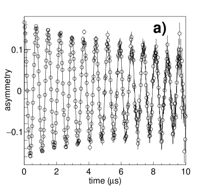
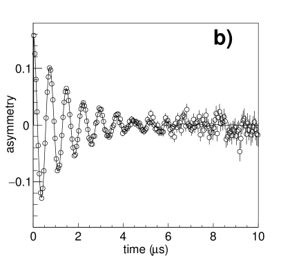
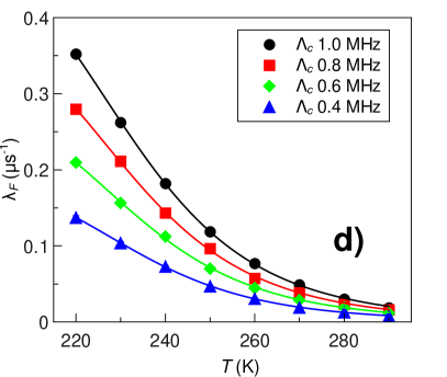
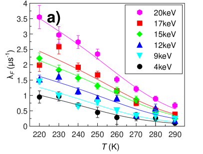
Figure 1 displays the simulation results in an applied transverse field of 10 mT. The increase of the depolarization rate with increasing hole capture rate is obvious from the SR asymmetry spectra in Fig. 1(a) and (b). Figure 1(c) demonstrates the linear relationship between hole carrier density - which determines the hole capture rate - and the emergent fast depolarization rate in the presence of charge cycles. Figures 1(c) and (d) show, that for a given , decreases with increasing temperature. This is due to the exponentially increasing Mu ionization rate, which means that the muons spend less and less time in the neutral state, causing less and less dephasing/depolarization of the muon spin during the charge cycles. The solid lines in Fig. 1(d) are fits of the equation
| (2) |
where MHz is the hyperfine coupling of Mu averaged over the temperature range 220 K – 290 K Lichti et al. (1999), and with T is the hyperfine magnetic field at the electron, with gyromagnetic ratio . Equation 2 is the expression for 1/, where 1/ is the depolarization rate in a longitudinal field (field applied parallel to the initial muon spin direction, LF-SR) Lichti et al. (1999); Chow et al. (1996, 1993). Due to the fact that in Ge the TF-SR depolarization rate caused by nuclear dipolar fields is small compared to , the TF-SR depolarization rate can be well approximated by 1/. This is further supported by the fact that the TF-SR simulated data in Fig. 1 d) are very well fitted by Eq. 2. Equation 2 will be used in the analysis of the depth dependent hole carrier profiles under illumination. The temperature dependence of is mainly determined by the exponential temperature dependence of , and to a lesser extent by and . With increasing temperature, is exponentially increasing, causing the decrease of .
III Experimental Details
The samples were commercial Ge (100) 2” wafers, 0.5-mm-thick, and nominally undoped, n- or p-type with doping ranges between cm-3 and cm-3, with relative uncertainties of 10% for n-type and 20% for p-type wafers, as specified by the suppliers (MTI Corporation, Richmond CA, United States, and Crystec GmbH, Berlin, Germany). The undoped sample was n-type with a doping of cm-3, as specified by the supplier.
The LE-SR experiments were carried out at the low-energy muons (LEM) facility at the E4 beam lineProkscha et al. (2008) of the Swiss Muon Source (SS, Paul Scherrer Institut, Villigen, Switzerland).
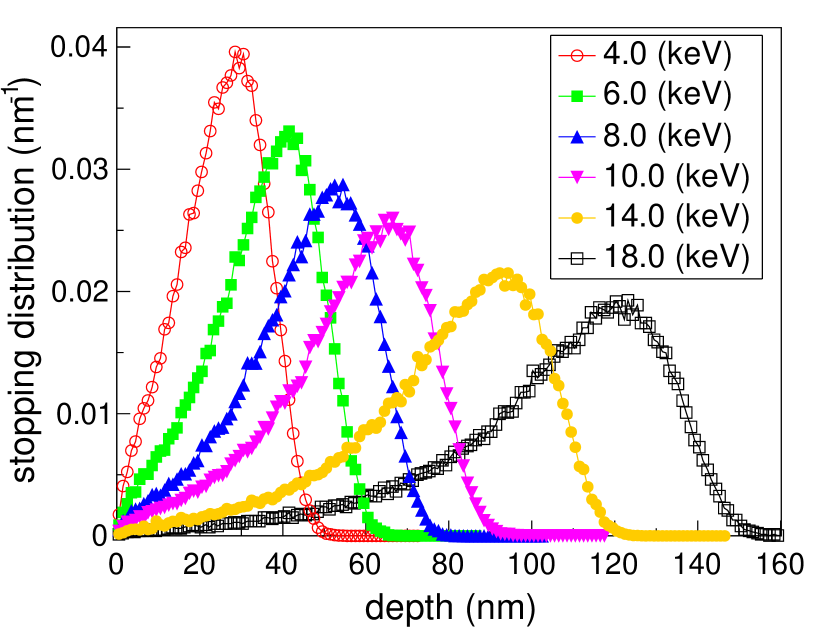
A beam of polarized with keV energies is generated by moderating a 4-MeV- beam, generated by the PSI proton accelerator, in a cryogenic moderator layer of solid Ar/N2Morenzoni et al. (1994, 2000); Prokscha et al. (2001). The moderated muons with eV energies are electrostatically accelerated up to 20 keV and transported by electrostatic elements to the sample region. The samples are glued with conductive silver paint on a Ag-coated sample plate made of aluminum, where the final implantation energy is adjusted by applying an electric potential up to kV to the sample plate. The implantation profiles of muons in Ge with energies between 4 and 18 keV are displayed in Fig. 2. To illuminate the samples, either LEDs or solid state lasers are available Prokscha et al. (2012, 2013); Stilp et al. (2014). For illumination with blue light we used either a LED source with nm (Bluepoint, Hönle AG, Gräfeling, Germany) or a diode pumped solid state laser with nm. For red light a diode laser with nm was used (both lasers from DelMar Photonics Inc San Diego CA, United States). In all cases the maximum light intensity at the sample was 50 - 100 mW/cm2.
In addition to the near-surface investigations with LE-, the bulk of the Ge wafers was studied at a mean depth of about 300 m employing the two instruments DOLLY and GPS Amato et al. (2017) which use 4-MeV-. The original wafers were cut in about 1 cm2 pieces to fit into the cryostats of the bulk-SR instruments. In all muon experiments the magnetic field was applied parallel to the direction, and transverse to the initial muon spin direction.
IV Results
IV.1 Diamagnetic fractions at different depths and doping levels
Figure 3 shows the temperature dependence of the diamagnetic fraction for various Ge samples with different doping levels and at different muon implantation energies, i.e. different mean depths of stopping . is defined as the fraction of muons in a diamagnetic state, determined by the fraction of muons precessing at the muons’ Larmor frequency.
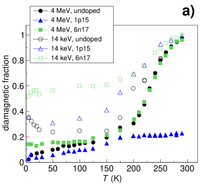
We begin with the description of the bulk SR measurements of the undoped and p- and n-type samples [ cm-3 (1p15), cm-3, (6n17)] in Fig. 3 a). The diamagnetic fraction is 20% at K, and either slowly increasing from 5 K to 150 K for the undoped and 1p15 sample, or nearly constant for the 6n17 sample. Such a weak increase of has been also reported in this temperature range for the samples of Ref. Fan et al. (2008) with doping levels cm-3. It can be understood as manifestation of the low-temperature formation of the Mu state through a transition state, as has been recently proposed as a general feature in the formation of the final muon configuration Vilão et al. (2017). In the n-type sample such an increase of diamagnetic fraction is not observed, and might be a consequence of the high electron concentration and/or a modification of the barriers in the transition state due to the doping of the lattice, favoring the formation of Mu already at low temperatures. It is important to note that these subtle effects do not affect the dynamics at K, where the dominant neutral fraction (Mu) becomes thermally ionized. The faster increase of between 150 K and 200 K can be attributed to the thermally activated ionization of Mu, which is “completed” at K Fan et al. (2008). This appears as a flattening of in the 1p15 sample: here the increase of due to the thermally activated formation of Mu at K is not observable - in contrast to the undoped and 6n17 sample - because the presence of holes drives the reverse reaction in Eq. 1 too quickly.
Implanting the muons much closer to the surface with an energy of 14 keV at a mean depth 80 nm reveals considerable differences: i), at K is significantly larger than in the bulk, ii), the increase of due to thermally activated Mu formation appears to begin at a lower temperature around 150 K, and iii), the most striking feature, we observe the thermally activated formation of Mu in the 1p15 sample. The latter can be explained by the absence of holes at least to a depth of 120 nm, i.e. the presence of a hole depletion layer. This is supported by the observed weak depolarization rate at 220 K, which is smaller than the expected depolarization rate of s-1 for cm-3 [Fig. 1 a)], implying cm-3 in the depletion layer. Additionally, the larger below 100 K indicates an electron accumulation in the near-surface region, with ranging between cm-3 and cm-3 Andrianov et al. (1978); Patterson (1988). This means that the 1p15 wafer exhibits a surface layer inversion, where hole depletion and electron accumulation are generated by band bending at the surface. The presence of free electrons in the accumulation region adds to the Mu formation rate due to thermal activation the electron capture rate of the process , yielding an enhanced Mu formation rate. This explains the larger values at K, and the lower temperature onset of the increase of , where the thermally activated Mu formation sets in ( K). The larger value of of the 1p15 sample compared to the undoped sample indicates a higher electron concentration or a larger band bending and accumulation of electrons in the p-type sample. The undoped sample is closer to insulating, implying weaker band bending compared to the p-type sample, i.e. a smaller electron accumulation.
The increase of in the undoped sample at K can be explained within the thermal spike model Vilão et al. (2019). Here, excess heat (due to energy liberated during the stopping process and also as a consequence of stress release to reach the final lattice configuration around the thermalized Mu0) may not be quickly enough released to the surrounding lattice due to a reduced thermal conductivity at low temperatures. This may cause thermal ionization of the Mu0, increasing the diamagnetic fraction. In the bulk of the sample, this effect obviously does not occur. In contrast, in the surface region with presumably larger lattice distortions Vilão et al. (2019), causing a reduced thermal conductivity, the thermal spike effect can explain the increase of .
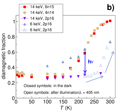
To further support the interpretation of a hole depletion layer, we show in Fig. 3 b) the results of a p-type sample with an order of magnitude larger hole concentration (2p16). We also present for comparison the temperature dependencies of two n-type samples which show similar trends as the undoped sample. In the 2p16 sample at 14 keV ( 80 nm) the thermally activated formation of Mu is no longer observed: does not increase at K, indicating that cm-3, or in other words the hole depletion layer is now significantly shifted towards the surface. This is confirmed on lowering to 6 keV ( 35 nm), where we again observe - as in the case of the 1p15 sample at 14 keV - the thermally activated formation Mu, which means that the hole depletion layer is still present, but with reduced width. Besides hole depletion the larger value of below 150 K compared to the n-type samples indicates electron accumulation.
IV.2 Hole carrier profile in the depletion region and its manipulation by illumination
As a first attempt to manipulate the depletion region we illuminated the 2p16 sample at 220 K with blue light ( nm) at an intensity of up to 80 mW/cm2. Upon light irradiation the value of measured at 220 K at 6 keV implantation energy is comparable to that measured at 14 keV implantation in the dark, indicating that the depletion region is removed, or at least significantly shifted towards the surface. After turning off the light, does not change, demonstrating the persistent change/removal of the depletion layer. This effect has been observed previouslyProkscha et al. (2013) and it is attributed to the trapping of photo-generated electrons in empty surface acceptor states, charging the surface negatively and thus pulling holes from the bulk and the photo-generated holes into the depletion region. On warming the sample in the dark, begins to increase at K, where trapped electrons from the surface acceptor states are released and move back into the bulk of the wafer where they recombine with holes, re-establishing the hole depletion zone. The release of the electrons appears as a thermally activated process with an energy barrier of about 1.1 eV Prokscha et al. (2013).
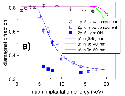
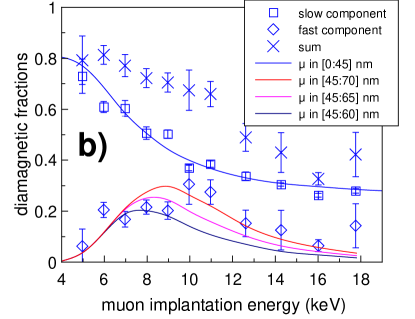
To determine the width of the depletion region in the two p-type samples we measured as a function of between 1 keV and 20 keV at K, see Fig. 4. In the 1p15 sample only the slowly relaxing component is observed, indicating cm-3 in the entire energy/depth range accessible by low-energy muons. The solid lines in Fig. 4 a) are from stopping profile simulations (see Appendix B) assuming an increase of to cm-3 beyond 140 and 150 nm, respectively. In this case, a fast component should appear, leading to a decrease of the slowly relaxing component. No sharp drop of is observed, excluding an increase of in this region. This implies, that the depletion width is larger than 160 nm, the maximum range of 20-keV in Ge. The observed weak decrease of can be explained by a slowly increasing activation energy for Mu ionization as a function of depth: the presence of an electric field due to the band bending in the depletion zone will result in a reduction of on approaching the surface, increasing the Mu ionization rate at a fixed temperature, which causes an increase of Prokscha et al. (2014). Below 5 keV both samples exhibit . In the 2p16 sample at keV, begins to drop, and the data can be well described by the solid line shown in the figure. This line is calculated assuming cm-3 at depths 45 nm, and the emergence of holes with cm-3 beyond 45 nm, which implies the appearance of a fast relaxing component . Indeed, we observe this fast component, changing as a function of implantation energy as shown in Fig. 4 b). The data can be best modeled by assuming a depth interval of [45:70] nm, where is in the range of cm-3 and cm-3. A larger cm-3 means a too fast depolarization of the SR signal, causing a loss of the observable . This explains the drop of the sum of both components as a function of : if the reach regions with , the fast component can no longer be observed leading to the reduction of as shown in Fig. 4 b). Figure 4 c) displays as a function of implantation energy, derived from the measured by scaling according to the simulation data of Fig. 1 c). It is in the expected range, but the errors are getting large at keV due to the decreasing and the relatively poor statistics of the data. Thus, no firm conclusions about the carrier profile in the depth range [45:70] nm can be drawn from this plot. Instead, we use simple modeling to calculate carrier profiles and determine the parameters of the model to obtain qualitative agreement with the experimental data. The hole carrier profile in the depletion region depends on the local band deformation at depth as Lueth (2010)
| (3) |
where is the bulk acceptor density of the p-type material, and , where is the electrostatic potential with its bulk value . Since there is actually not only depletion but inversion at the surface, we can assume that the surface potential determining the band bending significantly exceeds , Lueth (2010). In this Schottky space-charge approximation the electrostatic potential decays quadratically from its surface value into the bulk following
| (4) |
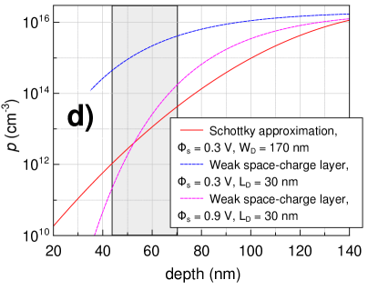
with a depletion width Sze and Ng (2006); Schroder (2006). Choosing nm, i.e. V, and inserting in Eq. 3 gives the red curve in Fig. 4 d), resulting in a hole carrier concentration in the shaded area ( nm) in the range of – cm-3, in good agreement with the experimental in Fig. 4 c). We note, that the Schottly approximation assumes for the free carrier densities , and complete ionization of the acceptors. Due to the electron accumulation in the hole depletion zone, , thus increasing the negative space charge in this region. For simplicity we assumed in the calibration , giving a total space charge . This seems to be justified by the fact that the bulk values of the two p-type samples seem to be the dominant densities to explain the observed differences in the depletion width estimates below.
For comparison and illustration, we show in Fig. 4 d) the blue curve in the weak space-charge limit for V (however, the weak space-charge limit is applicable for , which is not fulfilled here) where
| (5) |
with the Debye length nm for the 2p16 sample at 220 K. In this case, would be in the range – cm-3, in contradiction to the experimental results. In order to bring into the experimentally observed range one would need to use an even larger V (magenta curve in Fig. 4 d)), clearly outside the weak space-charge approximation.
The findings of Fig. 4 can be summarized as follows. The data are well described within the Schottky approximation, implying an abrupt change of from cm-3 to cm-3 within about 20 nm commencing at a depth of 45 nm. After illumination with blue light at 220 K, a persistent hole accumulation with cm-3 is established in the depletion region at implantation energies between 6 keV and 14 keV, corresponding to a range of nm to nm. In the 1p15 sample the width of the depletion layer is estimated to nm, times larger than for the 2p16 sample (the width of the depletion layer scales with the square root of the bulk carrier concentration Sze and Ng (2006)). We estimate the space charge density for the two samples to cm-2 for the 2p16 sample, and cm-2 for the 1p15 sample.
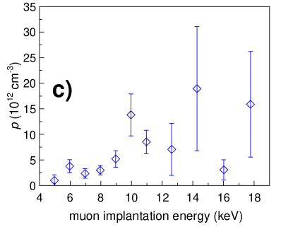
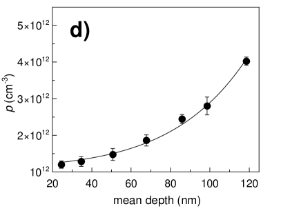
Now we turn to the manipulation of in the wide depletion region of the 1p15 sample by illumination with red light ( nm). Under illumination, again a fast component appears, indicating the presence of photo-generated holes in the depletion zone. However, after turning off the light the fast component disappears and the original slow component fraction is restored, meaning that the photo-generated holes in the depletion zone immediately disappear by recombination. This suggests, that the photo-electrons generated by red light do not have enough energy to overcome the eV barrier at the surface to reach the empty surface acceptor states. In this case, a dynamic equilibrium of photo-generated holes and electrons is established in the depletion region, and a quick recombination with photo-generated electrons takes place after turning off the light. As shown in Fig. 5 a), the fast component can be tracked in the temperature range from 220 K to 290 K, and from close to the surface at 4 keV ( nm) to a mean depth of 120 nm at 20 keV. This is different to illumination with blue light, where after an illumination time of 3 min with a laser (instead of the weaker LED source) at nm and mW/cm2, the fast depolarization rate exceeds values of 60 s-1 ( cm-3), which is the maximum detectable depolarization rate within the experimental resolution of the LEM apparatus. The fast component can no longer be resolved, and it appears as a “missing” fraction in the SR spectra, as in Fig. 4 b). In contrast, the dynamic equilibrium photo-generated hole carrier concentration with red light is significantly smaller, with in the order of cm-3, as we will show below.
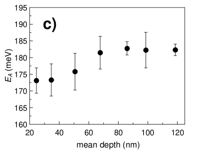
The increase of as a function of energy in Fig. 5 a) points towards an increasing hole carrier concentration with increasing depth. For a quantitative analysis we used Eq. 2 to fit the data (solid lines in Fig. 5 a)). In the fits we fixed according to Appendix A i), the exponent of the temperature dependence of to -2.2 [], ii), the pre-factor in the ionization rate to s-1, and iii), MHz, which is the average value of the hyperfine coupling of Mu in the temperature range between 220 K and 290 K Lichti et al. (1999). The value of is within the range of s-1 and s-1 of pre-factors found in Ref. Lichti et al. (1999). The free fit parameters were and the activation energy , which are displayed in Figs. 5 b) and c), respectively. From the hole carrier concentration ) as a function of mean depth is calculated in Fig. 5 d), using the re-analyzed calibration data of Ref. Prokscha (2014) in Appendix A. In doing so we assume that the measured at implantation energy equals at the corresponding mean depth. The justification for the validity of this assumption is discussed in Appendix C.
Figure 5 c) indicates a change of by about 10 meV under illumination between the near-surface region and a depth of about 80 nm, where it reaches its bulk value. This indicates a rather weak band bending under illumination with an electric field mV/nm, where is reduced by meV Prokscha et al. (2014). According to Fig. 5 d), the electric field is becoming too weak to change within errors in regions where cm-3. These electric field values are confirmed by fitting Eq. 3 in the Schottky approximation to the data in Fig. 5 d). In order to obtain a good fit we added a constant offset term to Eq. 3, where we attribute the appearance of to the non-equilibrium situation under illumination. The fit yields a depletion width nm, which is significantly smaller than the estimated nm for the dark sample. A lowering of under illumination is expected due to the reduction of band bending by the partial compensation of the surface charge by the photo-generated charge carriers. Using the reduced value of in Eq. 4 gives an electric field of mV/nm at a depth of 80 nm, in good agreement with the expected value estimated above.
V Discussion
By means of low-energy SR we determined directly the free charge carrier profile at the surface of a semiconductor. Knowing , the electrostatic potential can be calculated using Poisson’s equation. A direct experimental determination of the bending of at the surface is possible by photoemission spectroscopy. However, this method is limited to the first few nanometers at the surface, i.e. to high bulk doping levels cm-3, because only in this case the depletion range is comparable to the photo-electron escape depth Yu and Cardona (2010). We note, that can be also determined directly by LE-SR in cases, where a change of Mu0 activation energies is observable Prokscha et al. (2014). In contrast to photoemission spectroscopy the sensitivity of LE-SR to free hole carrier concentrations is orders of magnitude larger in Ge: as low as cm-3 can be detected by LE-SR over a hundred times longer length scale of about 200 nm with a resolution of a few nanometers. This resolution exceeds significantly the capabilities of capacitance-voltage techniques, where due to the Debye-length limitation it is not possible to profile closer than about 1 to the surface Schroder (2006), which is nm in the 2p16 sample, and nm in the 1p15 sample.
The high sensitivity to holes in the Mu Mu reaction is due to the large hole capture cross section cm2 of Mu, where we estimate using the relation with MHz (corresponding to cm-3) as a lower detection threshold [Fig. 1 a)], and a hole velocity cm/s.
We now turn to the implications of our results on the surface charge. The observed hole depletion and electron accumulation signifies a positively charged surface, suggesting the presence of empty, positively charged donor states. The change of the surface charge to negative under illumination with blue light requires the existence of empty surface acceptor states, which are persistently filled by photo-generated electrons. With red light, no persistent charging occurs, because the photo-generated electrons do not have enough energy to overcome the surface barrier of about 1.1 eV Prokscha et al. (2013). The observed electron accumulation even for the 6n17 sample means that surface donor states are still not filled with electrons, implying that these donor states must be located close to the conduction band - otherwise, they would be filled and neutral. The surface acceptor states, filled under blue illumination, must also be similarly high in energy as the surface donor states - otherwise, they would be filled as well at 6n17 doping, leading to a negative surface charge, and thus changing the band bending to remove electron accumulation. For a cleaved Ge surface without oxide layer it is well established that Fermi level pinning exists close to the valence band, causing an upward band bending at the Ge surface with hole accumulation and electron depletion Kuzmin et al. (2016); Dimoulas and Tsipas (2009); Kuzum et al. (2009); Gobeli and Allen (1964). This is different to our commercial Ge wafers with a nanometer-thin native oxide layer. The oxide can exist in various oxidation states GeOx which may strongly affect the electronic properities/band bending of the Ge/GeOx interface Kuzum et al. (2008); Schmeisser et al. (1986). The prevailing oxidation state for native oxide is +4 (GeO2), with the presence of GeOx with at the Ge/GeO2 interface Sahari et al. (2011). Assuming that the band structure at the interface is determined by the band alignment of GeO2 with a band gap of eV and a conduction band offset eV with respect to Ge Ohta et al. (2006), we speculate that i), the band bending in Ge at the Ge/GeO2 interface is opposite to a cleaved Ge surface, yielding electron accumulation and hole depletion as illustrated for isotype heterojunctions in Ref. Sze and Ng (2006), and ii), the surface energy barrier is determined by . While the details of the Ge/GeO2 interface are important for device applications, its more detailed characterization is out of the scope of this study and remains for upcoming work. Here, our intention is to demonstrate the capability of charge carrier profiling in the near-surface region of a semiconductor which allows getting insights also in the surface characteristics.
VI Conclusions
We demonstrated that, by means of a contact-less, non-destructive local probe technique, the free charge carrier concentration profile can be determined directly over a depth range from close to the surface up to 160 nm. We have shown by low-energy SR that charge carrier profiles at semiconductor interfaces can be directly studied with nanometer depth resolution, if a muonium state forms in the semiconductor that is interacting with free carriers. The sensitivity of the technique depends on the cross section of carrier capture by the muonium state. In the case of Ge it is the interaction of the Mu state with holes at K which is utilized for this purpose, where hole carrier concentrations can be determined in the range cm-3 by the measureable effect on the muon spin depolarization rate in transverse magnetic field. This allowed us to determine the hole carrier profile and its light induced manipulation in the hole depletion/electron accumulation region at the surface of commercial Ge wafers with a thin native GeO2 layer on top.
As an outlook, the method can be applied to characterize on a microscopic level the properties of the GeOx/Ge interface which might yield new insights for technologically relevant Ge device applications. The study of pre-cleaned surfaces, where the native oxide layer has been removed, would be interesting to provide complementary quantitative information on a nanometer scale of the expected hole accumulation due the Fermi level pinning close to the valence band.
Acknowledgements.
We gratefully acknowledge the help of P. Biswas and H. Luetkens in setting up the DOLLY and GPS experiments, and we thank H.P. Weber for his technical support in the operation of the LEM facility. The SR measurements were performed at the Swiss Muon Source SS, Paul Scherrer Institut, Villigen, Switzerland. The SR data were analyzed using the program musrfit Suter et al. (2012).Appendix A Ionization and hole capture rate parameters of the 1p15 sample
In Ref. Prokscha (2014) we used the p-type sample with cm-3 (1p15) to determine , , and the exponent of the temperature dependence of . Longitudinal field scan data at temperatures between 220 K and 290 K were fit with Eq. 2 with fixed s-1 and fixed hyperfine coupling constant of Mu at its low temperature value of 2.36 GHz. Since depends on temperature we re-analysed the data of Ref. Prokscha (2014) with a reduced GHz in the temperature range 220 K – 290 K, and with a free parameter in the ionization rate . This procedure yields slightly different values of the ionization and hole capture rate parameters compared to Ref. Prokscha (2014). These are s-1, meV, s-1, and exponent of the temperature dependence of .
Appendix B Simulation of diamagnetic fractions
We use a simple model to calculate the diamagnetic fractions in Fig. 4. The fraction of muons with implantation energy , stopping in a given depth interval , is calculated using the simulated muon stopping profiles (see Fig. 2). For the slow component, is then given by
| (6) |
where we use the fact, that at 220 K in the absence of holes, and is the offset diamagnetic fraction, which does not originate from the thermally activated ionization of Mu. Correspondingly, for the fast component in Fig. 4 b) we use
| (7) |
where is the diamagnetic fraction of muons at 220 K originating from thermally activated ionization of Mu, and which interact with holes.
Appendix C Depolarization function of a sum of depth dependent exponential depolarization functions
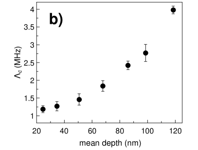
The measured , where is a constant. In the case of a depth dependent the depolarization rate will become a function of depth as well, . This means that the depolarization function of an ensemble of muons with a stopping distribution is an integral of exponentials weighted by . A sum of exponentials can be approximated by a stretched exponential function Johnston (2006). However, in our case the experimental data can be well fitted by a single exponential depolarization function. To test the validity of using a single exponential depolarization function, we added the SR data of energies {4,6,9,12,15,17,20} keV, where the average energy is 11.9 keV. The mean depth of the sum of stopping distributions is 69.3 nm, which agrees well with the mean depth of the single 12 keV data with nm. The sum spectrum is very well fitted with a exponential depolarization function with a reduced of 0.96 with 2036 degrees of freedom, strongly supporting the single exponential function model, where of the summed data agrees within statistical error with of the 12 keV single energy data. The same result is obtained when choosing a different set of data, e.g. {12,15,17,20} keV, where of the sum spectra with an average energy of 16 keV equals the of a single energy of 16 keV. This has the important implication that the measured , which is the average of ’s across the muon stopping profile, reflects at the mean stopping depth, i.e. . In other words, , justifying the interpretation of the data, that the for a given muon implantation energy reflects the hole carrier concentration at the corresponding mean depth .
References
- Sze and Ng (2006) S. M. Sze and K. K. Ng, Physics of Semiconductor Devices (John Wiley & Sons, Inc., Hoboken, NJ, USA, 2006), 3rd ed.
- Schroder (2006) D. K. Schroder, Semiconductor Material and Device characterization (John Wiley & Sons, Inc., Hoboken, NJ, USA, 2006), 3rd ed.
- Ferry (2013) D. Ferry, Semiconductors (IOP Publishing Ltd, 2013).
- Patterson (1988) B. D. Patterson, Muonium States in Semiconductors, Reviews of Modern Physics 60, 69 (1988).
- Cox (2009) S. F. J. Cox, Muonium as a Model for Interstitial Hydrogen in the Semiconducting and Semimetallic Elements, Reports on Progress in Physics 72, 116501 (2009).
- Yaouanc and Dalmas de Réotier (2011) A. Yaouanc and P. Dalmas de Réotier, Muon Spin Rotation, Relaxation, and Resonance: Applications to Condensed Matter (Oxford University Press, Oxford, UK, 2011).
- Prokscha et al. (2013) T. Prokscha, K. H. Chow, E. Stilp, A. Suter, H. Luetkens, E. Morenzoni, G. J. Nieuwenhuys, Z. Salman, and R. Scheuermann, Photo-Induced Persistent Inversion of Germanium in a 200-nm-deep Surface Region, Scientific Reports 3, 2569 (2013).
- Prokscha et al. (2014) T. Prokscha, H. Luetkens, E. Morenzoni, G. J. Nieuwenhuys, A. Suter, M. Döbeli, M. Horisberger, and E. Pomjakushina, Depth Dependence of the Ionization Energy of Shallow Hydrogen States in ZnO and CdS, Physical Review B 90, 235303 (2014).
- Holzschuh (1983) E. Holzschuh, Direct Measurement of Muonium Hyperfine Frequencies in Si and Ge, Physical Review B 27, 102 (1983).
- Lichti et al. (1999) R. L. Lichti, S. F. J. Cox, K. H. Chow, E. A. Davis, T. L. Estle, B. Hitti, E. Mytilineou, and C. Schwab, Charge-State Transitions of Muonium in Germanium, Physical Review B 60, 1734 (1999).
- Fan et al. (2008) I. Fan, K. H. Chow, B. Hitti, R. Scheuermann, A. I. Mansour, W. A. MacFarlane, B. E. Schultz, M. Egilmez, J. Jung, Y. G. Celebi, H. N. Bani-Salameh, B. R. Carroll, J. E. Vernon, and R. L. Lichti, Influence of Photoexcitation on the Diamagnetic Muonium States in Ge Studied via their Precession Signatures, et al., Physical Review B 78, 153203 (2008).
- Andrianov et al. (1978) D. G. Andrianov, G. G. Myasishcheva, Y. V. Obukhov, V. S. Roganov, G. I. Savelev, V. G. Firsov, and V. I. Fistul, Interaction of Muonium with Atoms in the Crystal Lattice of Germanium, Soviet Physics Semiconductors 12, 92 (1978).
- Lichti et al. (2008) R. L. Lichti, K. H. Chow, and S. F. J. Cox, Hydrogen Defect-Level Pinning in Semiconductors: The Muonium Equivalent, Physical Review Letters 101, 136403 (2008).
- Prokscha (2014) T. Prokscha, Simulation of TF-SR Histograms in Germanium in the Presence of Cyclic Charge State Transitions of Muonium, Journal of Physics: Conference Series 551, 012049 (2014).
- Kadono et al. (1997) \BibitemOpen\bibfieldauthor R. Kadono, R. M. Macrae, K. Nishiyama, and K. Nagamine, Evidence for muonium passivation in n-doped Ge, \bibfieldjournal Physical Review B 55, 4035 (1997).
- Prokscha (2012) T. Prokscha, Monte-Carlo Simulation of Transitions between Different Muonium States, Physics Procedia 30, 50 (2012).
- Chow et al. (1996) K. H. Chow, B. Hitti, R. F. Kiefl, S. R. Dunsiger, R. L. Lichti, and T. L. Estle, Diffusion and Charge Dynamics of Negatively Charged Muonium in n-Type GaAs, Physical Review Letters 76, 3790 (1996).
- Chow et al. (1993) K. H. Chow, R. F. Kiefl, J. W. Schneider, B. Hitti, T. L. Estle, R. L. Lichti, C. Schwab, R. C. DuVarney, S. R. Kreitzman, W. A. MacFarlane, et al., Muonium Dynamics in Si at High Temperatures, Physical Review B 47, 16004 (1993).
- Prokscha et al. (2008) T. Prokscha, E. Morenzoni, K. Deiters, F. Foroughi, D. George, R. Kobler, A. Suter, and V. Vrankovic, The New E4 Beam at PSI: A Hybrid-Type Large Acceptance Channel for the Generation of a High Intensity Surface-Muon Beam, Nuclear Instruments and Methods in Physics Research Section A 595, 317 (2008).
- Eckstein (1991) W. Eckstein, Computer Simulation of Ion-Solid Interactions (Springer, Berlin, Heidelberg, New York, 1991).
- Morenzoni et al. (2002) E. Morenzoni, H. Glückler, T. Prokscha, R. Khasanov, H. Luetkens, M. Birke, E. M. Forgan, C. Niedermayer, and M. Pleines, Implantation Studies of keV Positive Muons in Thin Metallic Layers, Nuclear Instruments and Methods in Physics Research Section B 192, 254 (2002).
- Morenzoni et al. (1994) E. Morenzoni, F. Kottmann, D. Maden, B. Matthias, M. Meyberg, T. Prokscha, T. Wutzke, and U. Zimmermann, Generation of Very Slow Polarized Positive Muons, Physical Review Letters 72, 2793 (1994).
- Morenzoni et al. (2000) E. Morenzoni, H. Glückler, T. Prokscha, H. P. Weber, E. M. Forgan, T. J. Jackson, H. Luetkens, C. Niedermayer, M. Pleines, M. Birke, et al., Low-Energy SR at PSI: Present and Future, Physica B: Condensed Matter 289-290, 653 (2000).
- Prokscha et al. (2001) T. Prokscha, E. Morenzoni, C. David, A. Hofer, H. Glückler, and L. Scandella, Moderator Gratings for the Generation of Epithermal Positive Muons, Applied Surface Science 172, 235 (2001).
- Prokscha et al. (2012) T. Prokscha, K. H. Chow, H. Luetkens, E. Morenzoni, G. Nieuwenhuys, Z. Salman, R. Scheuermann, A. Suter, and H. P. Weber, Low-Energy SR Investigations of Photo-Induced Effects on a nm Scale, Physics Procedia 30, 219 (2012).
- Stilp et al. (2014) E. Stilp, A. Suter, T. Prokscha, Z. Salman, E. Morenzoni, H. Keller, P. Pahlke, R. Hühne, C. Bernhard, R. Liang, et al., Controlling the Near-Surface Superfluid Density in Underdoped YBa2Cu3O6+x by Photo-Illumination, Scientific Reports 4 (2014).
- Amato et al. (2017) A. Amato, H. Luetkens, K. Sedlak, A. Stoykov, R. Scheuermann, M. Elender, A. Raselli, and D. Graf, The New Versatile General Purpose Surface-Muon Instrument (GPS) Based on Silicon Photomultipliers for SR Measurements on a Continuous-Wave Beam, Review of Scientific Instruments 88, 093301 (2017).
- Vilão et al. (2017) \BibitemOpen\bibfieldauthor R. C. Vilão, R. B. L. Vieira, H. V. Alberto, J. M. Gil, and A. Weidinger, Role of the transition state in muon implantation, \bibfieldjournal Physical Review B 96, 195205 (2017).
- Vilão et al. (2019) \BibitemOpen\bibfieldauthor R. C. Vilão, H. V. Alberto, J. M. Gil, and A. Weidinger, Thermal spike in muon implantation, \bibfieldjournal Physical Review B 99, 195206 (2019).
- Lueth (2010) H. Lueth, Solid Surfaces, Interfaces and Thin Films (Springer, Berlin Heidelberg, 2010), 5th ed.
- Yu and Cardona (2010) P. Y. Yu and M. Cardona, Fundamentals of Semiconductors: Physics and Materials Properties (Springer, Heidelberg Dordrecht London New York, 2010), 4th ed.
- Kuzmin et al. (2016) M. Kuzmin, P. Laukkanen, J. Makela, M. Tuominen, M. Yasir, J. Dahl, M. P. J. Punkkinen, and K. Kokko, Origin of Fermi-level Pinning and its Control on the n-Type Ge(100) Surface, Physical Review B 94, 035421 (2016).
- Dimoulas and Tsipas (2009) A. Dimoulas and P. Tsipas, Germanium Surface and Interfaces (Invited Paper), Microelectronic Engineering 86, 1577 (2009).
- Kuzum et al. (2009) D. Kuzum, K. Martens, T. Krishnamohan, and K. C. Saraswat, Characteristics of Surface States and Charge Neutrality Level in Ge, Applied Physics Letters 95, 252101 (2009).
- Gobeli and Allen (1964) G. W. Gobeli and F. G. Allen, Photoelectric Properties and Work function of Cleaved Germanium Surfaces, Surface Science 2, 402 (1964).
- Kuzum et al. (2008) D. Kuzum, T. Krishnamohan, A. J. Pethe, A. K. Okyay, Y. Oshima, Y. Sun, J. P. McVittie, P. A. Pianetta, P. C. McIntyre, and K. C. Saraswat, Ge-Interface Engineering With Ozone Oxidation for Low Interface-State Density, IEEE Electron Device Letters 29, 328 (2008).
- Schmeisser et al. (1986) D. Schmeisser, R. D. Schnell, A. Bogen, F. J. Himpsel, D. Rieger, G. Landgren, and J. F. Morar, Surface Oxidation States of Germanium, Surface Science 172, 455 (1986).
- Sahari et al. (2011) S. K. Sahari, H. Murakami, T. Fujioka, T. Bando, A. Ohta, K. Makihara, S. Higashi, and S. Miyazaki, Native Oxidation Growth on Ge(111) and (100) Surfaces, Japanese Journal of Applied Physics 50, 04DA12 (2011).
- Ohta et al. (2006) A. Ohta, H. Nakagawa, H. Murakami, S. Higashi, and S. Miyazaki, Photoemission Study of Ultrathin GeO2/Ge Heterostructures Formed by UV-O3 Oxidation, e-Journal of Surface Science and Nanotechnology 4, 174 (2006).
- Johnston (2006) D. C. Johnston, Stretched Exponential Relaxation Arising from a Continuous Sum of Exponential Decays, Physical Review B 74, 184430 (2006).
- Suter et al. (2012) A. Suter and B. M. Wojek, Musrfit: A free platform-independent framework for SR data analysis, Physics Procedia 30, 69 (2012).