11email: samantha.walker-1@colorado.edu
1 University of Colorado Boulder, Boulder, CO, USA
2 National Institute of Standards and Technology, Boulder, CO, USA
3 University of Michigan, Ann Arbor, MI, USA
Demonstration of 220/280 GHz Multichroic Feedhorn-Coupled TES Polarimeter
Abstract
We describe the design and measurement of feedhorn-coupled, transition-edge sensor (TES) polarimeters with two passbands centered at 220 GHz and 280 GHz, intended for observations of the cosmic microwave background. Each pixel couples polarized light in two linear polarizations by use of a planar orthomode transducer and senses power via four TES bolometers, one for each band in each linear polarization. Previous designs of this detector architecture incorporated passbands from 27 GHz to 220 GHz; we now demonstrate this technology at frequencies up to 315 GHz. Observational passbands are defined with an on-chip diplexer, and Fourier-transform-spectrometer measurements are in excellent agreement with simulations. We find coupling from feedhorn to TES bolometer using a cryogenic, temperature-controlled thermal source. We determine the optical efficiency of our device is () for 220 (280) GHz, relative to the designed passband shapes. Lastly, we compare two power-termination schemes commonly used in wide-bandwidth millimeter-wave polarimeters and find equal performance in terms of optical efficiency and passband shape.
Keywords:
feedhorn, polarimeter, microwave, millimeter-wave, cosmic microwave background, CMB, transition-edge sensor, TES1 Introduction
The cosmic microwave background (CMB) provides a powerful probe of the earliest moments of the universe. Precision measurements of CMB temperature and polarization aniso-tropies have played a crucial role in shaping our understanding of how the universe formed by providing rigorous constraints planck2018vi on parameters of the standard cosmological model, CDM. However, millimeter-wave observations are complicated by the presence of astrophysical foregrounds, such as synchrotron emission and galactic dust, which also radiate at these wavelengths. By designing detectors with broad spectral coverage, these foregrounds can be separated from the CMB because their spectral energy distributions are distinct. In addition, these detectors maximize the usage of telescope focal planes. For these reasons, several research groups are developing multichroic detectors mcmahon2012 with different coupling architectures suzuki2012 ; anderson2018 ; dahal2019 . We are developing feedhorn-coupled transition-edge sensor (TES) polarimeters, which have been deployed in multiple experiments ho2017 ; choi2018 ; koopman2018 over bands from 27 GHz to 220 GHz. In this work, we describe our first implementation of multichroic, dual-polarization-sensitive 220/280 GHz detectors for the Simons Observatory so2019 .
2 Design and Simulated Performance
We have designed and fabricated single-pixel, feedhorn-coupled, 220/280 GHz polarimeters. Devices were fabricated in the NIST Boulder Microfabrication Facility. The general feedhorn-coupled architecture is described by McMahon et al. mcmahon2012 . Fabrication is described in more detail by Duff et al. duff2016 . Here we focus on aspects unique to this design. The device consists of four optically-coupled TES bolometers for passband measurements in two linear polarizations. Additionally, we include two dark TES bolometers for systematic checks. TESs consist of an AlMn alloy and were designed to have = mK and = 8 m. Detector pixels were also designed with two different bolometer-saturation powers (). The first type has TESs with continuous membranes suitable for room-temperature Fourier-transform-spectrometer (FTS) measurements. The second type has TESs with released membranes suitable for ground-based photon loading in the Atacama Desert, Chile. Fig. 1 shows an optical micrograph of the detector pixel with components highlighted.
As part of our first implementation, we also designed each polarization with a different power-termination: a hybrid tee coupled to a lossy Au distributed termination (‘A-type’) chuss2012 or a PdAu lumped termination resistor (‘B-type’) myers2005 . The function of this termination is to dissipate only the lowest-order waveguide mode, TE11, on the bolometer. At 2.3:1 bandwidth, the planar orthomode transducer (OMT) supports multiple waveguide modes; however, we only wish to couple the bolometer to the TE11 mode because it exhibits a well defined polarization state. Furthermore, coupling the bolometer to higher-order modes is undesirable as it degrades angular resolution hubmayr2018 . In the A-type, filtered passbands are routed to a hybrid tee, which takes the input from two ports and produces sum and difference outputs. Higher-order modes are associated with the sum output and are terminated on the substrate, while power in the TE11 mode associated with the difference port is routed to the bolometer and dissipated in a lossy Nb-to-Au meander. In the B-type, a lumped termination resistor, thermally connected to the TES, is differentially fed signals from one pair of OMT probes. This termination scheme also results in a smaller bolometer than in the A-type, which could be beneficial for more tightly packed pixels.
The performance of the components listed in Fig. 1 was verified through electromagnetic (EM) simulations in Microwave Office (1D, www.awr.com), Sonnet (2.5D, www.-sonnetsoftware.com/), and HFSS (3D, www.ansys.com). We created a full 3D model in HFSS of the OMT (Fig. 1a), including a backshort and waveguide coupling. We calculated the scattering parameters of five waveports, one for the waveguide input and one for each of the four OMT probes. This model assumed no loss so that any power not found in these five waveports was assumed to be due to radiation that could leak out of the 25 m gaps between the planar OMT above and below the waveguide. From this, we predict 95.4% (89.6%) co-polar coupling, 2.4% (2.8%) reflection, and 2.2% (7.6%) radiation, averaged over the 220 (280) GHz passband. The co-planar waveguide-to-microstrip (CPW-to-MS) transition (Fig. 1b) was optimized with a transmission-line model in Microwave Office and then verified in Sonnet. Mean reflection across the extended passband, 195 GHz to 315 GHz, was simulated to be dB. The diplexer (Fig. 1c) was designed and verified in Sonnet. We estimate 94.7% (91.0%) transmission assuming SiN loss tangent (tan ) = 0.0008, averaged over the 220 (280) GHz passband. For the A-type termination, separate hybrid tees (Fig. 1d) were designed in Sonnet for the 220 GHz and 280 GHz passbands, because they have intrinsically narrow bandwidths. From the scattering parameters, the differential-odd mode, associated with the difference port, was calculated to have 99% transmission for each type. The Nb-to-Au transition (Fig. 1e), like the CPW-to-MS transition, was optimized with a transmission-line model in Microwave Office and verified in Sonnet. Mean reflection across the extended passband was simulated to be dB. For the B-type termination, the termination resistor (Fig. 1f) was simulated in Sonnet, assuming PdAu with sheet resistance /square and an ideal aspect ratio of length:width 7:1. Mean reflection across the extended passband was simulated to be dB.
3 Experimental Setup
To test the devices, we packaged the dies in brass split-block modules coupled to prototype aluminum spline-profiled feedhorns simon2016 , coupled to a time-division multiplexer (TDM) doriese2016 , and installed in a 100 mK adiabatic-demagnetization-refrigerator cryostat. We configured the cryostat in two ways for our two measurements. For measurement of detector passbands, we installed an optical-access window in the cryostat and used a Fourier-transform-spectrometer (FTS). The optical path from FTS to feedhorn consists of the following filters. At 300 K, we use a 8.89 cm diameter aperture stop and 5.08 cm thick polypropylene-based, expanded foam access window. At 50 K, we use a 2 cm thick single-layer anti-reflection (AR) coated PTFE filter. This AR coating has been optimized for transmission from 195 GHz to 420 GHz. At 4 K, we use a 14 cm-1 metal-mesh low pass filter ade2006 from Cardiff, a 1 cm thick Teflon filter, and a 1.5875 mm thick nylon stack with the same AR coating as the 50 K component. For measurement of detector optical efficiency, we used a cryogenic temperature-controlled thermal source heat-sunk to the 4 K stage. This thermal load consists of a 101.6 mm tesselating terahertz tile that has dB reflection at 300 GHz saily2004 . We therefore assume a perfect blackbody in our loading calculation discussed in the next section. Two uncalibrated thermometers on the backside of this thermal load are used to measure temperature changes. The source’s exponential decay-time constant was measured to be minutes. We place 14 cm-1 and 11 cm-1 low pass filters from Cardiff at 4 K to further attenuate any out-of-band pickup.
4 Results
4.1 Passbands
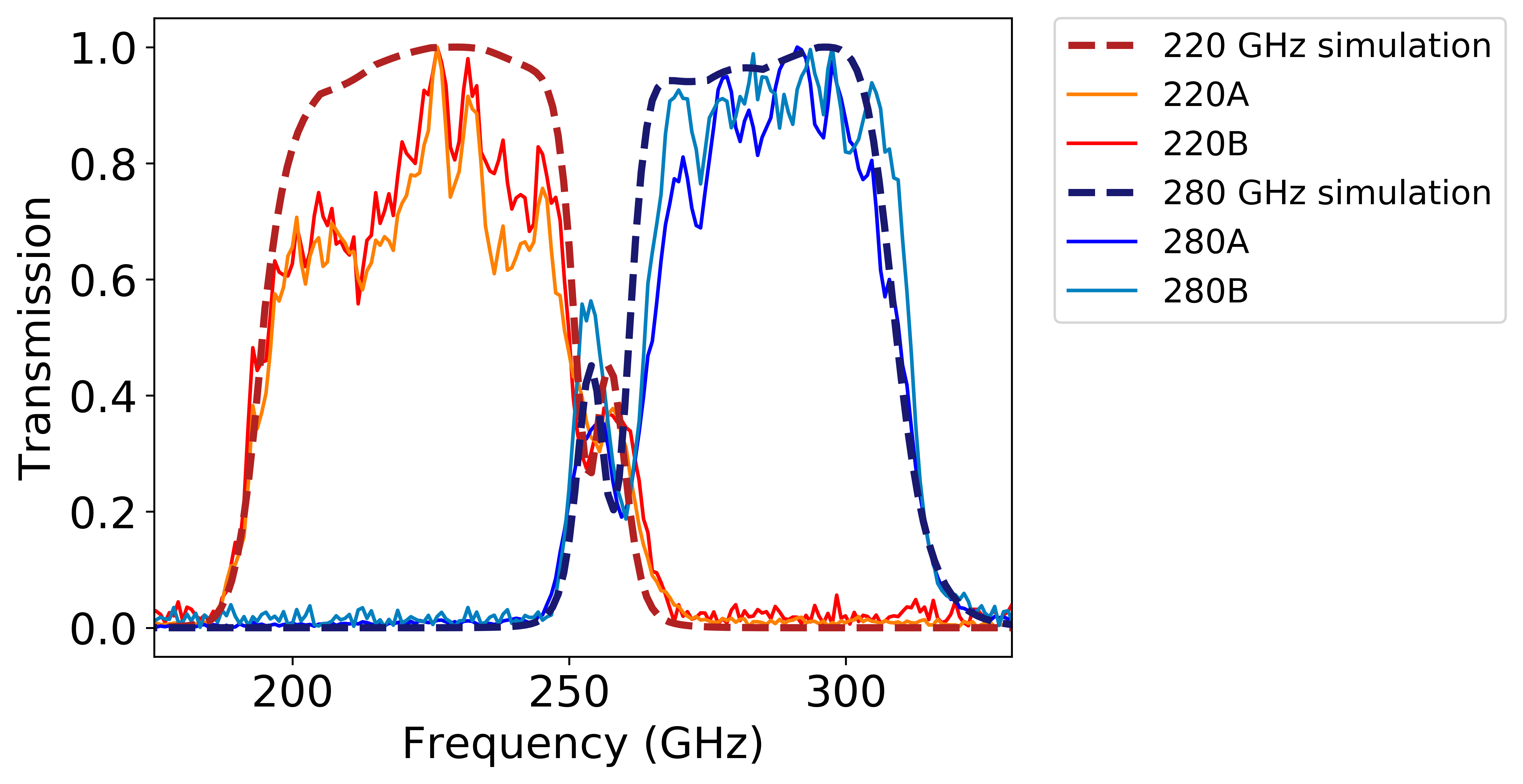
Fig. 2 shows peak normalized FTS measurements of the 220/280 GHz detector along with separate 220 GHz and 280 GHz simulations that consist of the simulated peak normalized frequency response of the diplexer and OMT. There is excellent agreement with simulations and both A- and B-type terminations give well-matched passbands. This agreement also shows that the slight interaction between the two passbands at 250 GHz is understood; this was removed with a simple design change in subsequent wafer production. Furthermore, the anti-reflection coating used in our filter stack is non-ideal. Given our knowledge of the materials and distances in the optical path from FTS to feedhorn, we expect fringing at the level of 20% to 30%, which is also seen in the data.
| Type | Raw | With dark subtraction |
|---|---|---|
| 220A | 95%1% | 76%2% |
| 220B | 97%4% | 79%6% |
| 280A | 97%4% | 72%4% |
| 280B | 103%3% | 78%4% |
4.2 Optical Efficiency
Because CMB measurements are inherently of low signal-to-noise ratio, we seek to maximize the optical efficiency of our detectors. We define optical efficiency as the ratio of the optical power dissipated in our TES bolometers () to the calculated loading power we would expect :
| (1) |
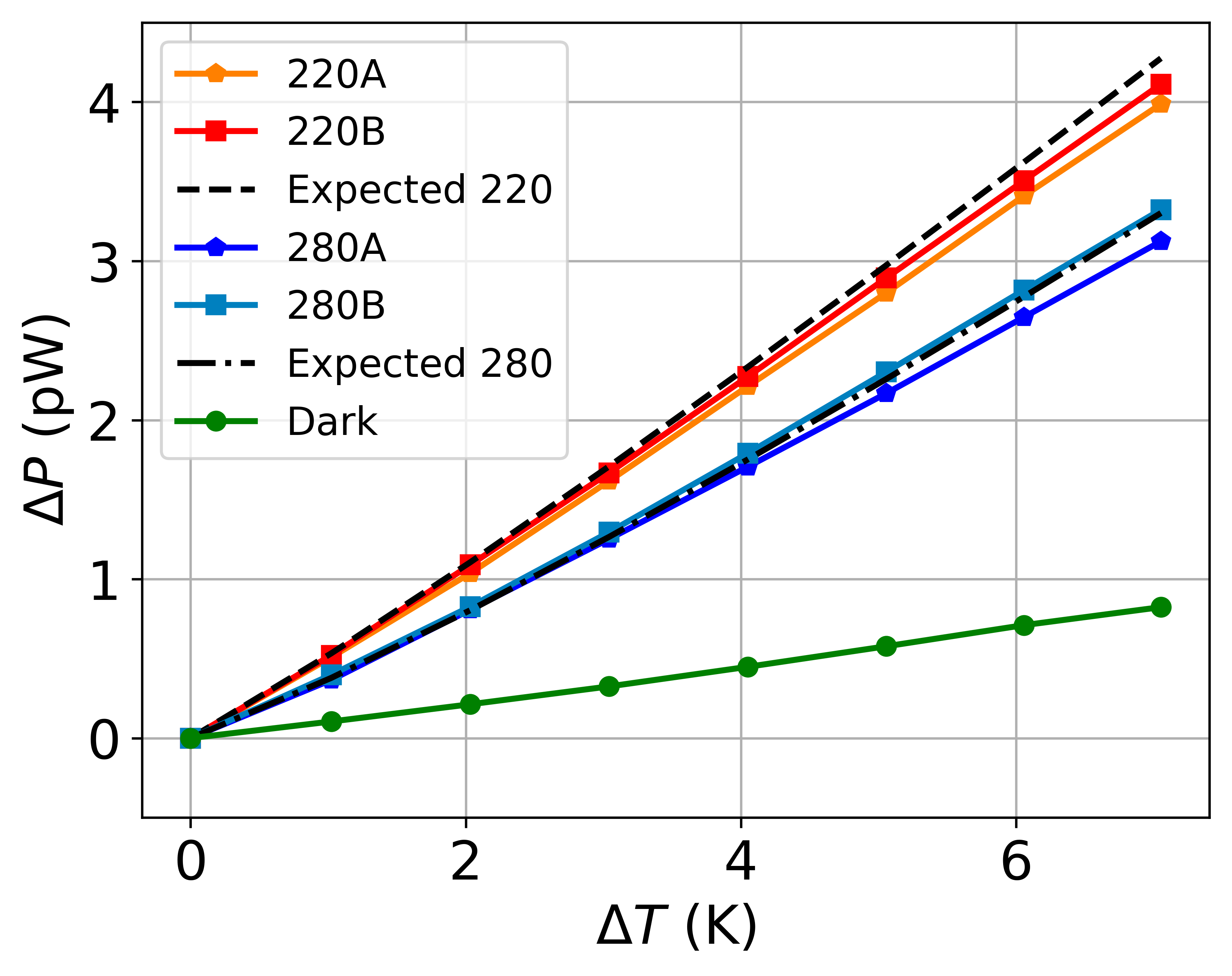
We vary the temperature of a beam-filling cryogenic blackbody load from 5 K to 12 K and measure the change in power in each TES through bolometer curves for at 80% . Measurements are taken at each 1 K point after 21 minutes to allow the thermal load to fully equilibrate. We calculate for a single mode and ideal blackbody, including simulated passbands and corrections for free space filter loss, as
| (2) |
where is the Planck constant, is frequency, is the Boltzmann constant, and is the blackbody temperature in kelvin. includes the peak normalized 220 GHz or 280 GHz simulated diplexer response, the peak normalized simulated OMT response, and the 300 K measured absolute transmission spectra of the 14 cm-1 and the 11 cm-1 low pass filters. Fig. 3 shows measurements of both optical and dark TES bolometer channels as a function of cryogenic blackbody temperature (referenced to 5 K) denoted by solid lines. Dashed lines correspond to calculations of expected loading power, , using Eq. (2).
Optical efficiencies are calculated with Eq. (1) for each point. The average is reported in Table 1, both with (‘With dark subtraction’) and without (‘Raw’) dark bolometer power subtraction. Error bars in Table 1 are the one standard deviation statistical uncertainty from 42 independent measurements, two pixels, seven points, and three repeats, summed in quadrature. Assuming the of dark bolometers accurately monitors the parasitic power radiatively coupled to the optically coupled bolometers, we subtract dark from optical to estimate . We calculate () for the 220 (280) GHz passband. Factors that could account for this additional loss include: imprecise knowledge of load temperature, ideal versus measured passband shape, uncertainty in the gap size of the OMT, and the dark subtraction assumption itself. Given these factors, there is general agreement between measurements and expectations.
5 Conclusions
We have demonstrated a working prototype of a multichroic feedhorn-coupled 220/280 GHz detector pixel through electromagnetic simulations, FTS passband measurements, and cryogenic temperature-controlled blackbody measurements to calculate optical efficiency. Measured passbands are in excellent agreement with simulations. We determine detector optical efficiency () for the 220 (280) GHz passband. These results are consistent with expectations and demonstrate efficient optical coupling from feedhorn to TES bolometer. As part of our first implementation of these devices, we also investigated two power-termination schemes commonly used in wide-bandwidth millimeter-wave polarimeters: a hybrid tee coupled to a lossy Au distributed termination (A-type) or a PdAu lumped termination resistor (B-type). We find equal performance in terms of optical efficiency and passband shape.
After testing a second prototype of this detector pixel, this design will be implemented in arrays to be fielded in the Simons Observatory. In arrays to be deployed, an all-silicon assembly will reduce the OMT waveguide gap by more than a factor of 2. This will result in both an expected increase in co-polar coupling and a decrease in leakage radiation, improving the optical performance beyond what we demonstrate here.
Acknowledgements.
This work was supported in part by the NASA APRA program, grant #NNX17AL23G. This material is based upon work supported by the National Science Foundation Graduate Research Fellowship under Grant No. DGE-1144083. Certain commercial software and materials are identified to specify the experimental study adequately. This does not imply endorsement by NIST nor that the software and materials are the best available for this purpose.References
- (1) Planck Collaboration, et al. arXiv e-prints, page arXiv:1807.06209, (2018).
- (2) J. McMahon, et al. Journal of Low Temperature Physics, 167(5-6):879–884, (2012).
- (3) A. Suzuki, et al. volume 8452 of Society of Photo-Optical Instrumentation Engineers (SPIE) Conference Series, page 84523H, (2012).
- (4) A. J. Anderson, et al. Journal of Low Temperature Physics, 193(5-6):1057–1065, (2018).
- (5) S. P. Ho, et al. volume 9914 of Society of Photo-Optical Instrumentation Engineers (SPIE) Conference Series, page 991418, (2017).
- (6) S. K. Choi, et al. Journal of Low Temperature Physics, 193(3-4):267–275, (2018).
- (7) B. J. Koopman, et al. Journal of Low Temperature Physics, 193(5-6):1103–1111, (2018).
- (8) P. Ade, et al. JCAP, 2019(2):056, (2019).
- (9) S. M. Duff, et al. Journal of Low Temperature Physics, 184(3-4):634–641, (2016).
- (10) D. T. Chuss, et al. Journal of Low Temperature Physics, 167(5-6):923–928, (2012).
- (11) M. J. Myers, et al. Applied Physics Letters, 86(11):114103, (2005).
- (12) J. Hubmayr, et al. Journal of Low Temperature Physics, 193(3-4):633–647, (2018).
- (13) S. M. Simon, et al. volume 9914 of Society of Photo-Optical Instrumentation Engineers (SPIE) Conference Series, page 991416, (2016).
- (14) W. B. Doriese, et al. Journal of Low Temperature Physics, 184(1-2):389–395, (2016).
- (15) P. A. R. Ade, G. Pisano, C. Tucker, and S. Weaver. volume 6275, page 62750U, (2006).
- (16) J. Säily and A. V. Räisänen. International Journal of Infrared and Millimeter Waves, 25(1):71–88, (2004).
- (17) S. Dahal, et al., Journal of Low Temperature Physics, This Special Issue (2019).