Linear impurity modes in an electrical lattice: Theory and Experiment
Abstract
We examine theoretically and experimentally the localized electrical modes existing in a bi-inductive electrical lattice containing a bulk or a surface capacitive impurity. By means of the formalism of lattice Green’s functions, we are able to obtain closed-form expressions for the frequencies of the impurity (bound-state) eigenmodes and for their associated spatial profiles. This affords us a systematic understanding of how these mode properties change as a function of the system parameters. We test these analytical results against experimental measurements, in both the bulk and surface cases, and find very good agreement. Lastly, we turn to a series of quench experiments, where either a parameter of the lattice or the lattice geometry itself is rapidly switched between two values or configurations. In all cases, we are able to naturally explain the results of such quench experiments from the larger analytical picture that emerges as a result of the detailed characterization of the impurity-mode solution branches.
I Introduction
In solid-state physics, it is a well established fact that lattices can feature localized modes in the presence of point defects, such as chemical impurities, vacancies or interstitials, that break the shift translational invariance of the perfect lattice Maradudin ; Lif . This type of disorder-induced localization can change the macroscopic properties of the crystal, its photon absorption spectrum (i.e., color) being a well-known example, but can also be responsible for a variety of interesting scattering phenomena marad . Related applications abound in a diverse array of themes, ranging from defect modes in photonic crystals Joann as well as optical waveguide arrays Pes_et99 ; Mor_et02 ; kipp to superconductors andreev , and from dielectric super-lattices with embedded defect layers soukoulis to electron-phonon interactions tsironis and granular crystals in materials science kavou .
A related theme that is of particular interest concerns the existence of localized modes at the surface (i.e., at the ends) of linear chains due to the finite size effect or, otherwise stated, the imposition of different kinds of boundary conditions. This type of exploration has also been a topic of consideration for over half a century, dating back to the early considerations of R.F. Wallis on the effects of free ends in one-dimensional wallis1d , as well as surface modes in two- and three-dimensional lattices wallis2d3d . It is remarkable that the relevant considerations continue to inspire recent work, either on the theoretical role of different types of boundary conditions luo , or on modern applications including those of phononic crystals jk that may also involve transversal-rotational modes tournas .
In the present work, we take advantage of the well established framework of electrical transmission lines remoissenet1 ; remoissenet2 as a prototypical setting where the theory of linear impurity modes can be tested. Upon modeling the experimental setting of recent experiments such as english1 ; english2 ; english3 at the linear level (i.e., in the absence of nonlinearity), we utilize the formulation of Green’s functions green1 ; green2 ; green3 in order to identify both the eigenvalues/eigenfrequencies and eigenfunctions of the linear modes of the lattice, focusing naturally on the localized vibrations thereof. We provide analytical expressions for these and a systematic comparison with the corresponding experimental results. This is done not only for the linear lattice with a defect, but also in the case of existence of a localized surface mode. Very good agreement is achieved between the two. Nevertheless, in addition to that, there are some interesting observations and twists offered. In particular, it is found that in each range of frequencies (i.e., both above and below the linear band), only one mode can be identified theoretically and observed experimentally. Additionally, quench type experiments are performed where we vary the parameter controlling the detuning from the homogeneous limit. In these we explore how the experimental lattice “jumps” from one value to the other and the lattice response accordingly transforms itself under such a quench. Finally, we also examine the voltage dynamics on the lattice during a switching transformation in its geometry from a line with an edge impurity into a ring with a bulk impurity.
Our presentation will be structured as follows. In section II, we will present the physical setup and mathematical model. In section III, we will provide details of the Green’s function formalism for identifying the corresponding localized modes. In section IV, we present our corresponding experimental results. Finally, in setion V, we summarize our conclusions and provide some directions for future study.
II The model
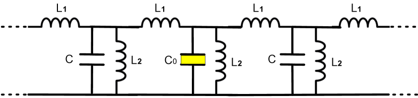
Our physical setup is that of remoissenet1 ; remoissenet2 (see also english1 ; english2 ; english3 for some recent experimental studies in this system). In particular, we consider the bi-inductive electrical lattice shown in Fig. 1. It consists on units composed of LC resonators coupled inductively by an inductor . If we call and , respectively the charge stored on the nth capacitor and the voltage drop across the inductor , the use of the Kirchhoff laws leads to a system of coupled equations
| (1) |
The impurity at the center of our current considerations is assumed to be a capacitive one located at , with capacitance . The rest of the capacitances are taken as identical and equal to . In other words, .
By taking and , we arrive at the stationary equations, i.e., the eigenvalue problem:
| (2) | |||||
where and is a dimensionless voltage, where is a characteristic voltage. By means of simple manipulations, we can rearrange Eq. (2) as
| (3) |
with
where , and .
Equation (3) describes formally a single impurity tight-binding model, whose Hamiltonian is given by
| (4) |
Using Dirac’s notation, we can express and in terms of Wannier functions as
| (5) |
the (undisturbed) lattice Hamiltonian, and
| (6) |
the defect (or impurity) Hamiltonian.
The Hamiltonian describes the lattice without the impurity and, as is well-known, possesses plane-wave eigenvectors
| (7) |
and eigenvalues
| (8) |
or, in terms of the electrical lattice parameters,
| (9) |
Thus, the system is able to support the propagation of electrical waves that form a band extending (in terms of ) from to . Notice that in the infinite lattice limit this band would be a continuous spectrum, while in the finite lattice case, the boundary conditions select a specific set of wavenumbers (e.g. with integer running up to for periodic boundary conditions), and thus only the corresponding frequencies are observed.
III The Green’s function formalism
Given a Hamiltonian , the lattice Green’s function is defined as green1 ; green2 ; green3
| (10) |
In our case, . Treating formally as a perturbation, we can express as
| (11) |
where is the unperturbed Green function. Inserting , we have
It can thus be easily proven that the eigen-energies of the localized modes are given by the poles of , while the probability amplitudes are given by the residues of at those poles.
III.1 Electrical impurity in the bulk
Let us consider a capacitive defect that is located far away from the boundaries of the system. In that case we have from green1 that:
| (12) |
After solving the energy equation , one obtains,
| (13) |
In terms of our electrical parameters, this leads to
| (14) |
where is the capacitive mismatch. However, it should be kept in mind that only one of the branches corresponds to each case: the one in Eq. (14) for or , and the one in Eq. (14) for or . Figure 2 shows the theoretically predicted energy branches as a function of the capacitive mismatch , for several different resonant frequencies . All eigenfrequencies lie outside of the band. In the absence of the defect, i.e., for , the solutions touch the band right at the edges of the band. These edge modes are the ones that detach from the band due to the presence of the defect.
For the bound state profile , we start from , where is the mode amplitude profile, and is given by the residue of at .
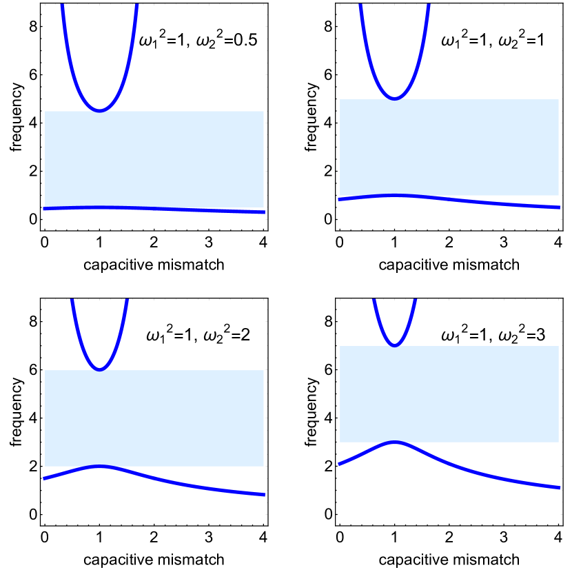
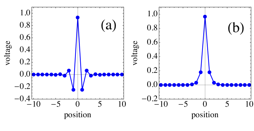
Figure 3 shows the spatial profile of the bound state for different electrical parameters, namely for and . The mode width decreases with either an increase in capacitive mismatch (associated with ) or an increase in frequency mismatch .
III.2 Electrical impurity at the boundary
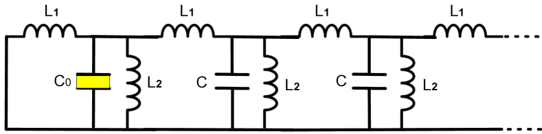
Now we consider the case where the defect is placed at the very surface of a semi-infinite electrical array (Fig. 4).
Computation of the proper Green’s function for this case requires realizing that, even though the main formalism is still the same as in section A, the unperturbed Green’s function needs to be computed by the method of mirror images: since there is no lattice to the left of , must vanish identically at . This means , where is the unperturbed Green’s function of the bulk case: . The procedure for computing the frequency of the surface bound state and its profile is exactly the same as in section III A, and it is detailed in the Appendix.
Figure 5 shows the eigenfrequency of the bound state as a function of the capacitive mismatch .
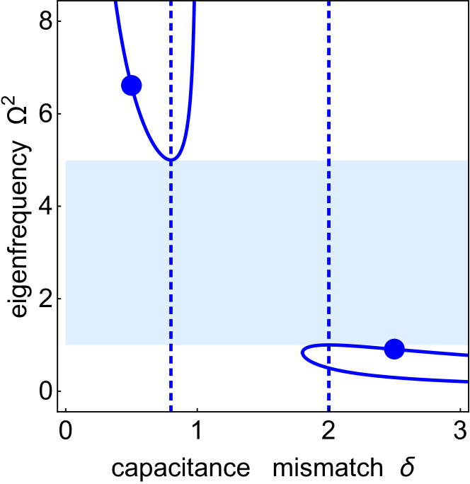
An interesting feature of in this case (with the boundary) concerns the forbidden bands inside which there are no bound states. In terms of frequencies, there exists the well-known frequency band that extends from up to . In terms of the parameter , there exists an interval in capacitive mismatch that extends from to
| (18) |
inside which the mode is complex. The most important intervals however, are the ones originating from the condition that the capacitance mismatch be sufficiently large to produce a bound state. These are given by and , where
| (19) |
The origin of this condition lies in the fact that the real part of the surface Green’s function, for outside the band, is bounded from above and below, unlike the case of the bulk Green’s function. Out of the different critical values only and are relevant since and . It can be also proven that at the energy curves touch the linear band. These features can be appreciated in Fig. 5.
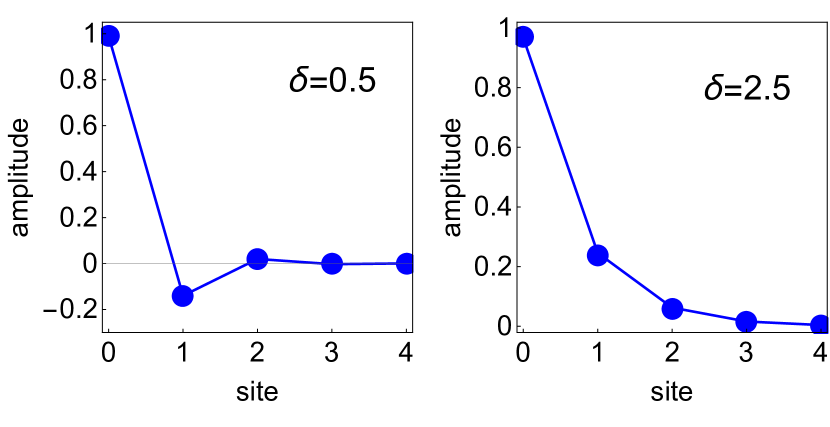
Figure 6 shows once again some spatial mode profiles. We now turn to the experimental realization of the above localized modes.
IV The experiment
We have built the bi-inductance lattice shown in Fig. 1 made up of discrete electrical elements of inductors and capacitors. The inductors were ferrite (radial-lead) inductors of 470 H inductance and about 1 resistance (ESR - equivalent series resistance). We used these inductors both as the and elements in a lattice with . The inductance values were all within 1 percent of one another. One set of measurements was also done on a lattice with , and there we also incorporated 975 H inductors with an ESR of 2 . The fixed capacitors, , were all of 1 nF capacitance, to within 2 percent of one another. In addition, in order to excite any mode we incorporated a driving signal using an arbitrary function generator (Agilent 33220A) whose signal was injected into the electrical lattice via 10 k resistors. The voltages at each lattice node were monitored using multi-channel DAQ boards (National Instruments PXI-6133).
The impurity was introduced via the replacement at one lattice site of the 1 nF capacitor with a varactor diode (NTE-618) whose capacitance can be continuously varied by applying a bias voltage. The capacitance-voltage relationship for the varactor diode was carefully mapped out by separately measuring the resonance curve of an RLC circuit that incorporated this diode in parallel with a known inductor. When introducing such a bias voltage across the varactor diode, care must be taken, however, to ensure that none of the inductors in the lattice experiences a DC potential drop across them. This was achieved by using a large (2 F) block capacitor in series with the varactor diode. In essence, then, we can continuously vary the -parameter with a DC power supply that controls the bias voltage across the varactor diode. This yields a capacitance range for from about 900 pF down to about 150 pF. Given our choice of nF, in order to attain the regime, we can place this varactor diode in parallel with a fixed 1 nF- or 2 nF capacitor.
IV.1 Impurity in the Lattice Bulk
To compare the experimental observations to the theoretical predictions in the previous section, Fig. 7(a) depicts the square of the normalized frequencies, as a function of the capacitance-mismatch parameter, , which measures the strength of the impurity, for the upper-branch localized modes. We see that the experimental data points (black circles) match the theoretical curve very well for the parameter values of and . Importantly, as we highlighted in the theoretical section only one of the two solutions with frequencies above the band is selected in line with the theoretical prediction. To excite these impurity modes, we can use a sinusoidal waveform that is swept through a range of frequencies while simultaneously recording the impurity mode response. In this way a spectrum is generated, and the mode frequency is obtained from the peak’s center frequency within that spectrum. The driving waveform can be applied uniformly at each site of the lattice, or alternatively only at the impurity site. Both driving methods yield the same frequency information, although the exact mode profile does depend slightly on the driving method. Here we show results corresponding to local driving.
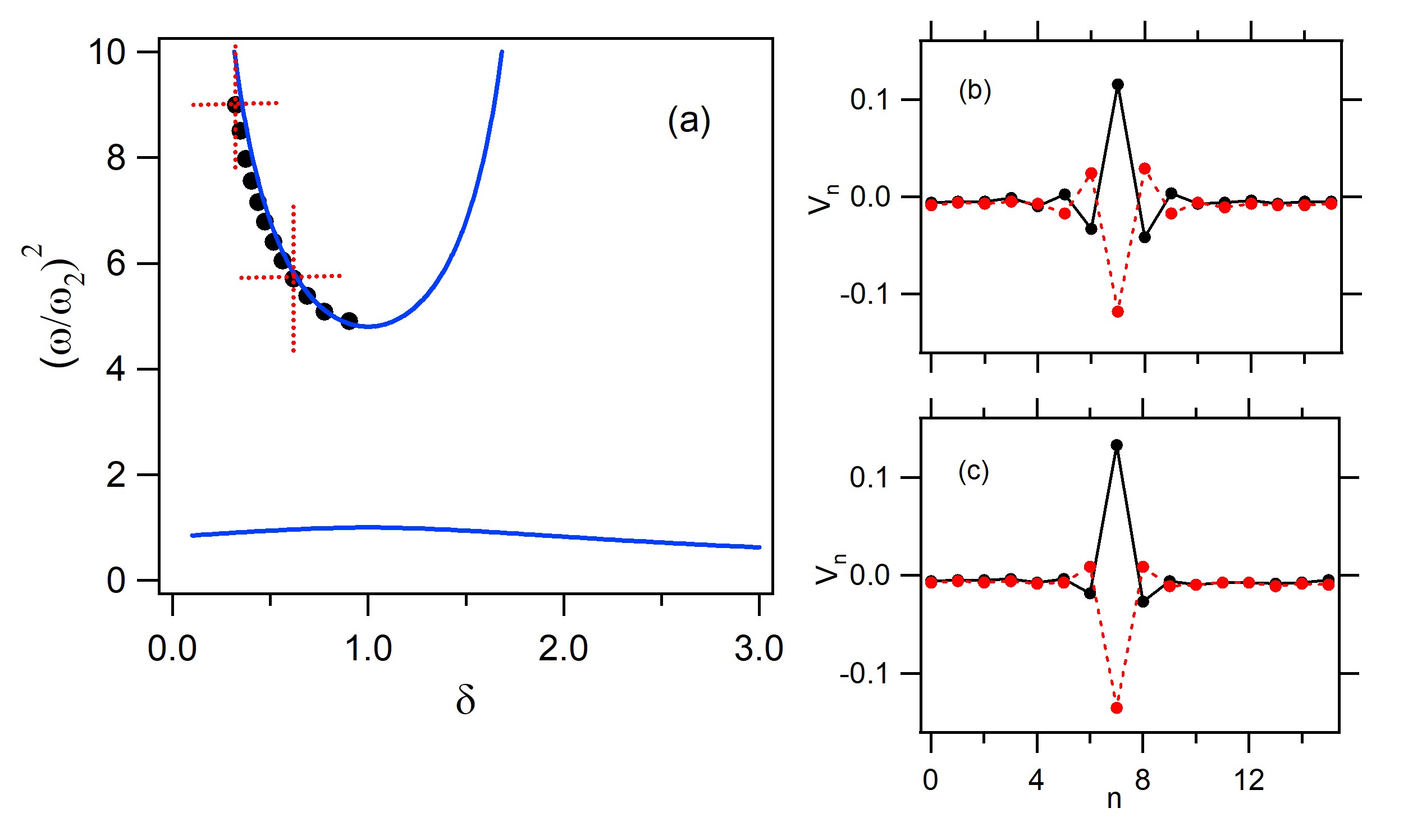
From the inductor values themselves, i.e., H, we would expect . The fact that this value is slightly lower in the experimental system, however, is confirmed independently by separately measuring the zone-boundary (ZB) mode frequency. Here a spatially staggered driver is employed to probe the resonance curve associated with the ZB mode, and its center frequency is recorded at around 502 kHz. Given that the zone-center mode is at 228 kHz, we would expect the ZB to be at approximately 510 kHz. The fact that it is found at somewhat lower frequency indicates that the effective is also lower by a small amount.
Figure panels 7(b) and (c) show the measured spatial profiles of two impurity modes, corresponding to and , respectively. The node voltages measured at two particular times are shown at which the voltage at the center node (n=7) is most positive and most negative, respectively. As also seen in the theoretical waveforms, the farther departs from 1, and thus the higher the frequency, the more localized the impurity mode is in space.
We now turn to the lower-branch modes in this lattice. From the theoretical picture of Fig. 2(b) and (c), we discern that when is raised relative to , the branch descends away from the bottom of the plane-wave spectrum more rapidly. (The same is also true in the case when is lowered relative to .) For this reason, we decided to decrease the coupling strength - and thus - while leaving unchanged when observing the lower branch. This was accomplished by using coupling inductors of H.
Figure 8 depicts the experimental results on the lower branch. The lines represent the theoretical curves given in Eq. (14), for and . We again see good agreement between theory and experiment, although some deviation is observed for -values close to 1, where the localized mode becomes quite broad (and where perhaps a larger lattice would thus be needed). Recall that per our theoretical analysis, only the portion of the branch with is physical (and thus experimentally traceable). The inset panel shows the impurity mode profile. We see that contrary to the upper-branch modes where neighboring sites oscillate out-of-phase, for these lower-branch impurity modes the nodes all oscillate in-phase. Thus, the impurity modes in both instances share the basic symmetry with that plane-wave mode into which they merge as .
IV.2 Impurity at the boundary
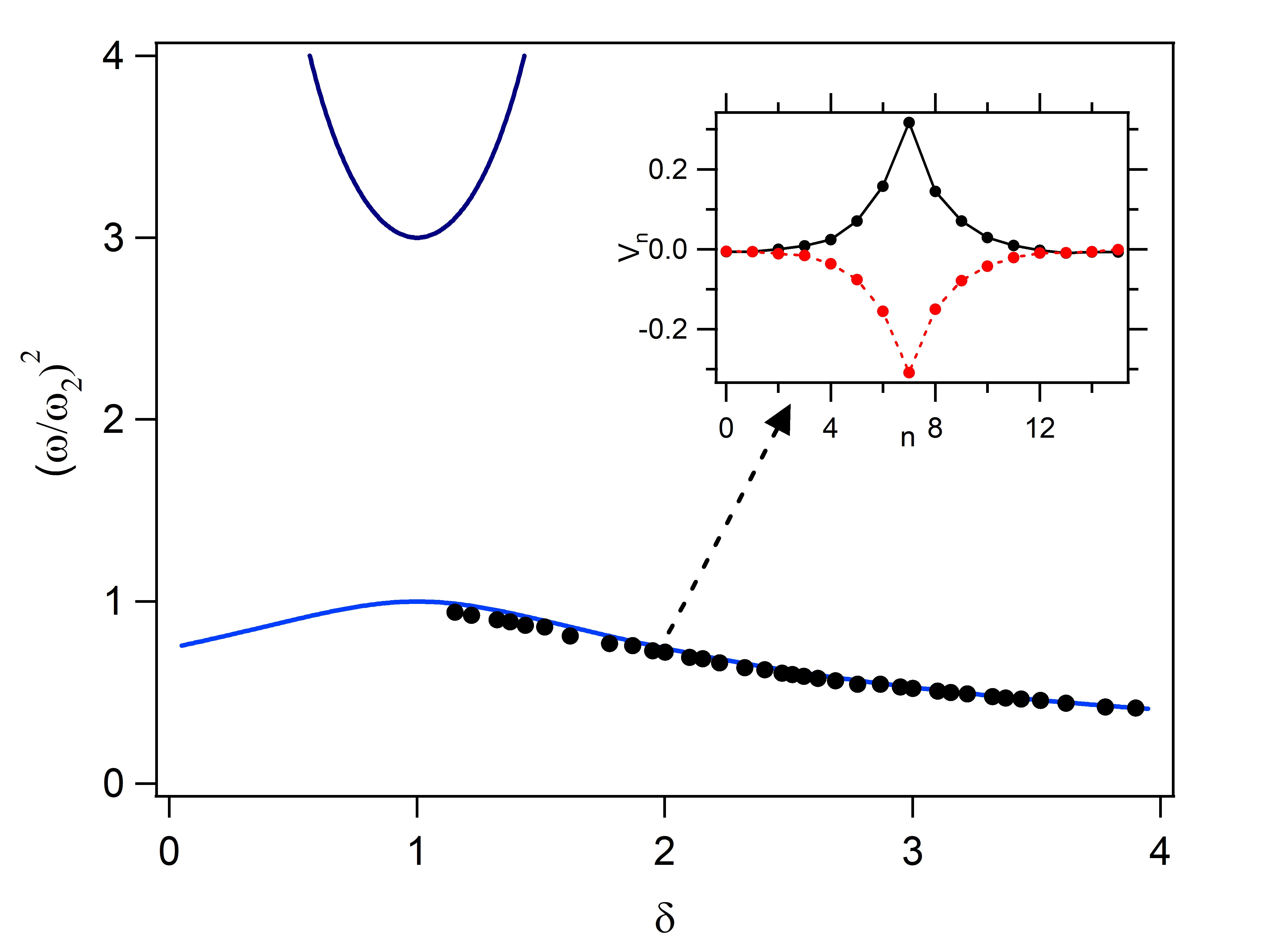
It is straightforward to transform the electrical lattice used so far into a lattice where the impurity is at its boundary. We simply disconnect the far end of the coupling inductor at n=7 and instead ground it. We also return to the case H, such that .
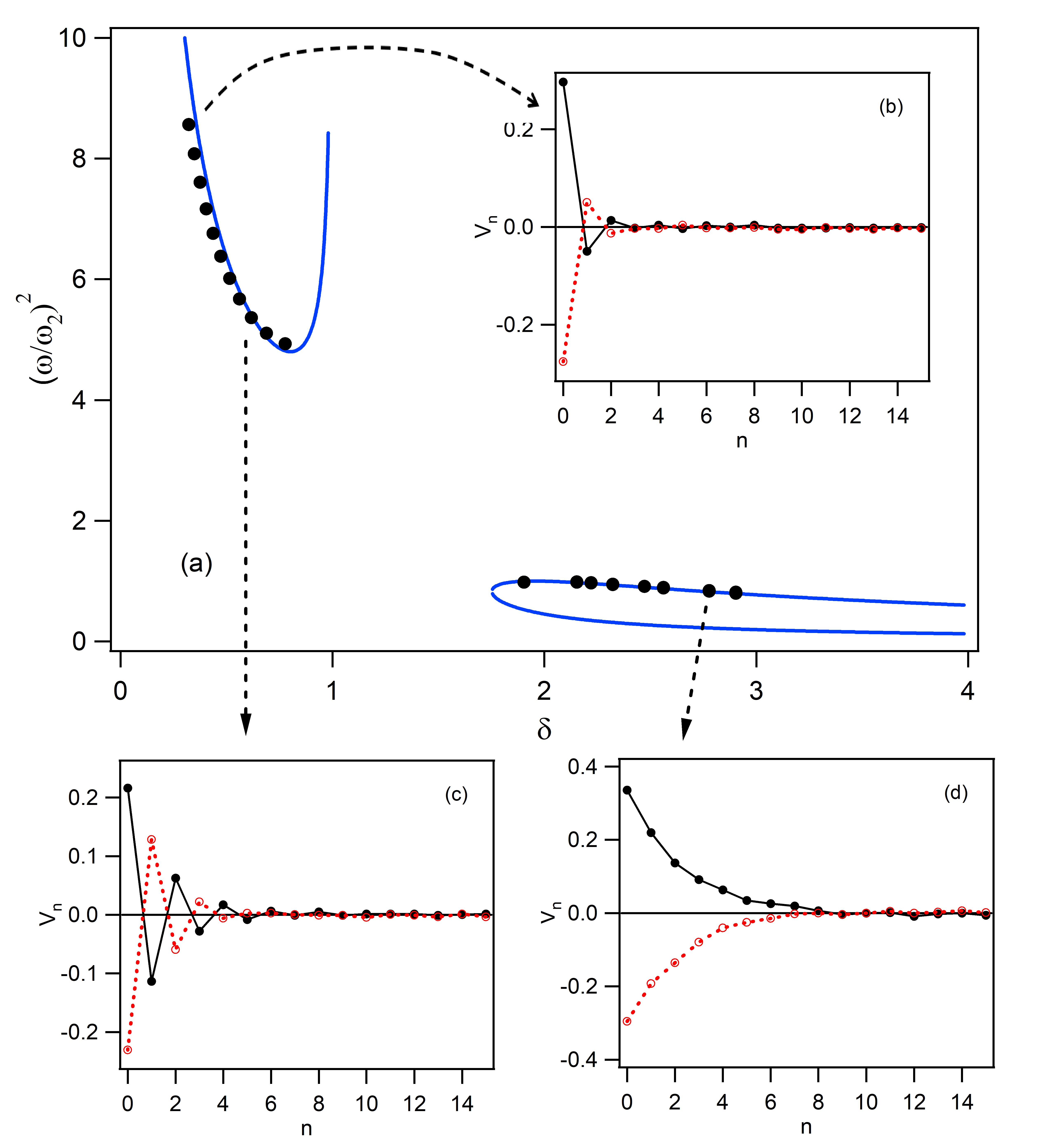
Confirming the theoretical prediction, no surface modes are found within the interval of . For , we observe upper-branch solutions, and for lower-branch solutions. Their frequencies nicely match the theoretical prediction, as seen in Fig. 9(a). Figure panels 9(b) and (c) show the spatial profiles of the upper-branch modes measured at the two -values of 0.32 and 0.62, respectively. As expected, we clearly observe the mode widening in space as approaches 1. Panel (d) depicts the lower-branch mode at . The width of the mode is somewhat larger than what is obtained in the analysis; one possible reason might be that experimentally, some part of the uniform mode may still be excited.
IV.3 Quench experiments
In order to examine the impact of quenches and the response of the system between the two fundamentally different regimes examined ( and in the bulk, and correspondingly also in the case of the surface), we devise the following quenching experiment. We use a single pole double throw (SPDT) analog switch, the chip ADG436, to rapidly switch between two capacitor values for : 0.57 nF and 1.43 nF. These two values were chosen because they are symmetrically situated relative to 1 nF. Again, the driving of the lattice can be either local (at the impurity) or the spatially homogenous (shown in the following figures). For the upper-branch case in Fig. 10(a), the driving frequency corresponded to (equivalent to 536 kHz). We see that at this frequency and for nF (corresponding to a of 0.57), the upper-branch impurity mode can be stably excited. When we abruptly switch to at time s, however, the mode disintegrates and does not reconstitute itself. That is to say, there is no corresponding physical branch on the other side at .
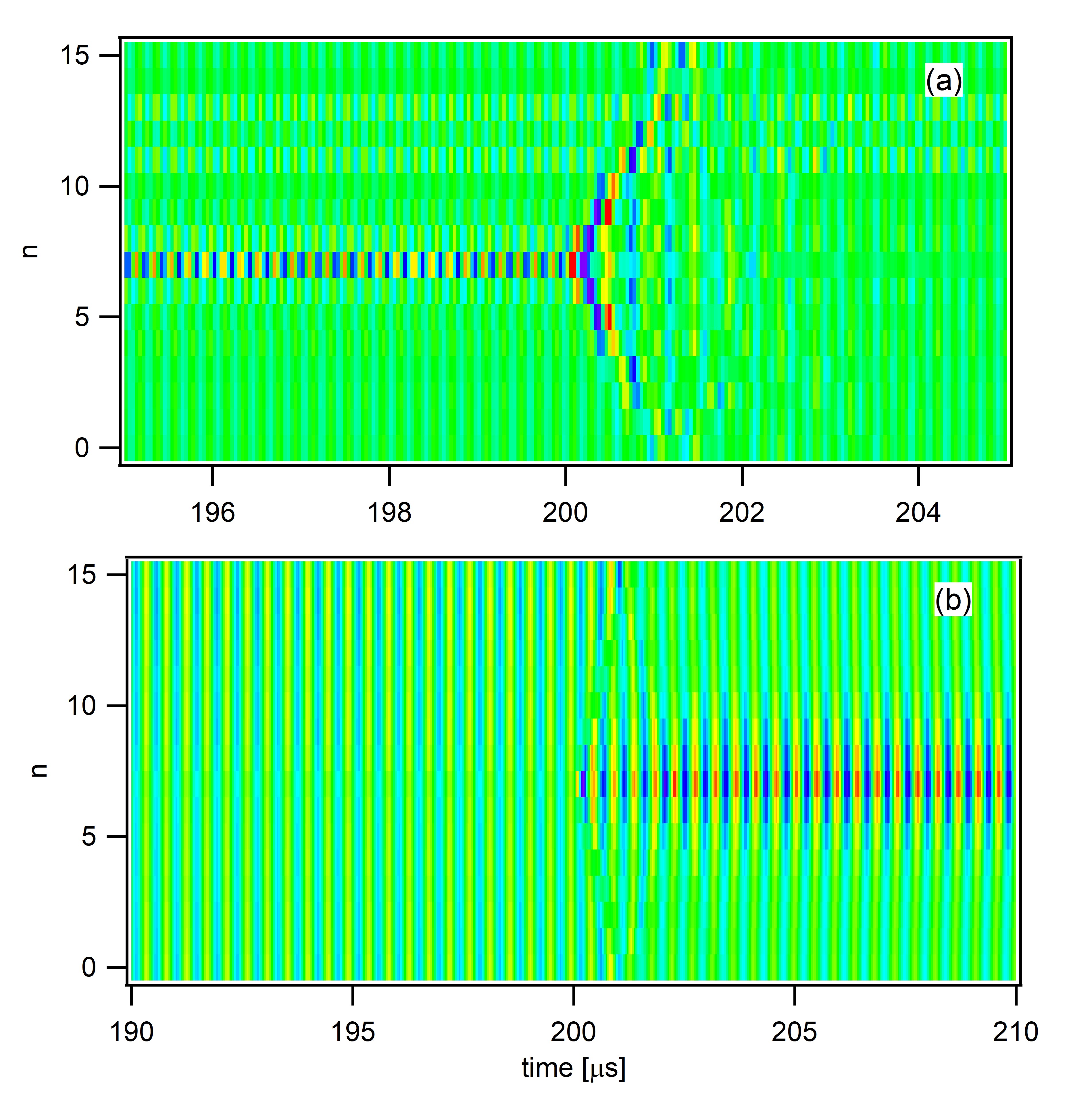
A similar phenomenon can be discerned in Fig. 10(b) for the lower branch, where we chose a frequency of 219 kHz (or ). Here no mode exists at , but upon abruptly switching to , the lower-branch impurity mode emerges. We should mention that if we start with the larger value of and then switch to the lower one, no impurity mode is generated in that case either.
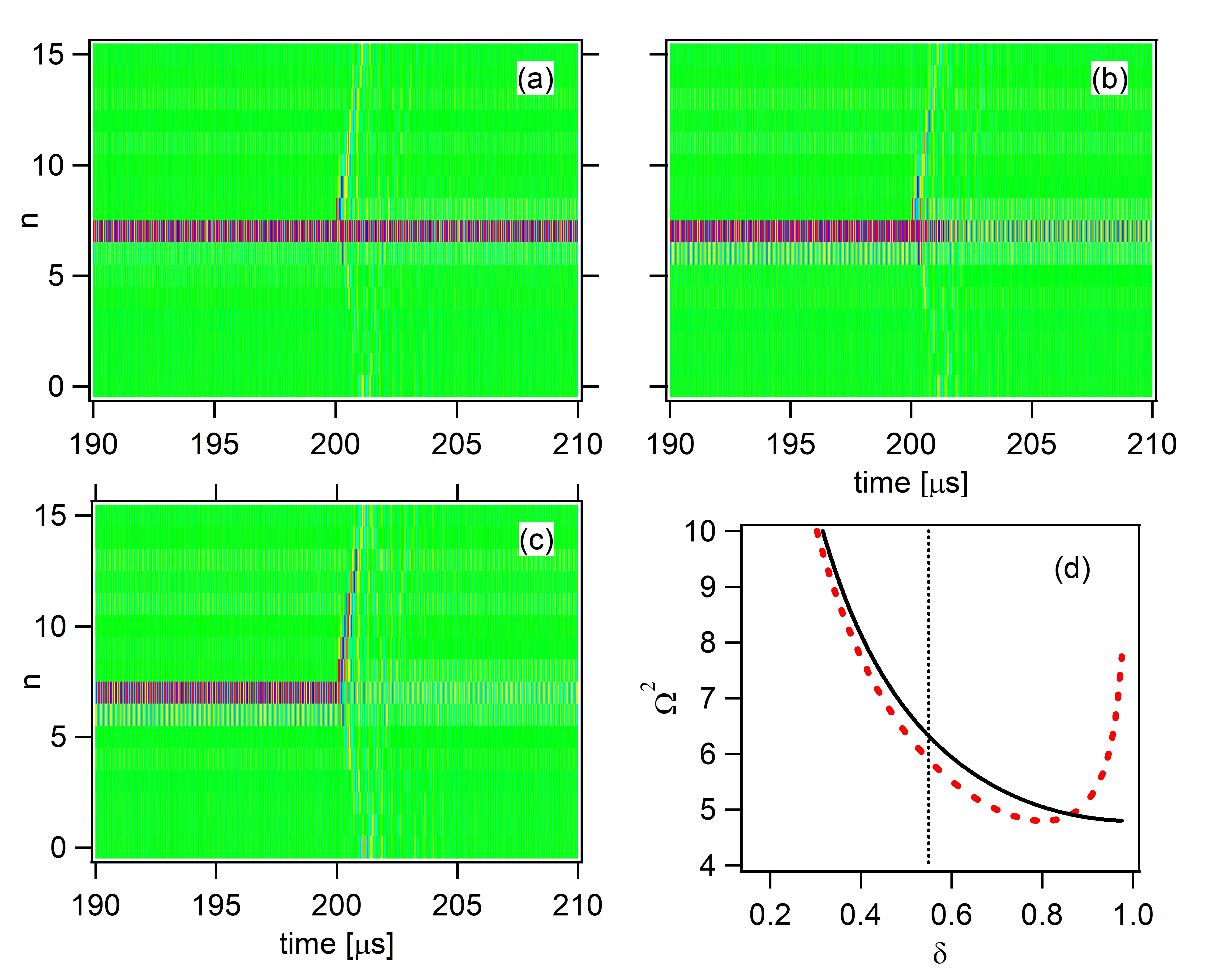
Another appealing switching experiment that can be performed in the present setting involves transforming the impurity mode from a surface one to a bulk one by using the analog switch to temporarily impose a boundary in the lattice that is otherwise ring-like. The switch connects the far end of the inductor at first to ground and then abruptly to the inductor at . Here we chose a of 0.47 and excited the lattice with a spatially homogenous driver at various upper-branch frequencies. This is illustrated in Fig. 11(a), where the frequency corresponds to . The switch from boundary lattice bearing a surface to a ring lattice (i.e., a bulk one with periodic boundary conditions) occurs at 200 s. We see that the initial surface mode naturally transforms itself into the bulk mode after the switch. Figure 11(b) and (c) decrease the driver frequency consecutively, to and 5.65, respectively. It is clear that the bulk mode is weakened in (b) and then disappears altogether in (c), while the surface mode is still generated at these frequencies.
This last result makes sense upon close comparison of Figs. 7(a) and 9(a), which (for convenience) is shown in Fig. 11(d). When superimposing the solution branches in the two cases, we see that the upper-branch surface modes have lower frequency compared to the bulk modes for all allowed -values of the former (i.e., for ). Since the experimental system features dissipation and thus potential relaxation to the modes, those modes have some width in frequency and therefore can overlap, such that at a given driving frequency both can be excited. However, if the driving frequency is repeatedly lowered, we first lose the bulk mode and only later the surface mode.
V Conclusions & Future Challenges
We have studied both theoretically and experimentally an electrical transmission-line lattice possessing a capacitive impurity point-defect located either at the bulk or at the boundary of the circuit. By using the formalism of lattice Green’s functions, we were able to predict the existence of localized modes for which the voltage decreases in space as we move away from the defect position. We obtained in closed form the bound-state frequency of the impurity state, as well as the bound-state profile as a function of the parameters of the electrical circuit. Very good agreement was observed between the theoretical predictions and the corresponding experimental results both for the bulk and also for the surface impurity modes. Additionally, quench-type experiments were performed, by rapidly switching a lattice parameter and observing how the voltage profile adapts itself to such a modification. Also an interesting scenario of a switch from a bulk lattice to a surface one was explored and the spontaneous transformation of the bulk modes to surface ones was elucidated. Such experiments were found to be in accord with the analytical picture characterized by its relevant solution branches.
Naturally, this study and the systematic benchmarking of the linear lattice properties paves the way towards further explorations. At the linear level, the theory of Green’s functions also permits an analytical characterization of the transmission problem from an impurity as a function of the wavenumber of the incoming wave, as well as of the impurity (and lattice) parameters. This is a technically more challenging problem as it arguably requires larger lattices than the ones considered herein, yet is, in principle, experimentally tractable. On the other hand, numerous studies have focused on nonlinear impurities in a linear lattice tsir1 ; moli ; ourmario as the first among the many different possible scenarios involving nonlinearity in the present setting. This is a natural next step for our studies, and will be considered in future publications.
Acknowledgements.
MIM acknowledges support from Fondo Nacional de Desarrollo Científico y Tecnológico (Fondecyt) Grant 1160177. PGK gratefully acknowledges support from NSF-DMS-1809074, the hospitality of the Mathematics Institute of the University of Oxford and the support of the Leverhulme Trust.References
- (1) A. A. Maradudin, E. W. Montroll, and G. H. Weiss, Theory of Lattice Dynamics in the Harmonic Approximation, Academic Press (New York, 1963).
- (2) I. M. Lifschitz, Nuovo Cimento, Suppl. 3, 716 (1956); I. M. Lifschitz and A. M. Kosevich, Rep. Progr. Phys. 29, 217 (1966).
- (3) A. A. Maradudin, Sol. Stat. Phys. 18, 273 (1966).
- (4) S. Y. Jin, E. Chow, V. Hietala, P. R. Villeneuve, and J. D. Joannopoulos, Science 282, 274 (1998); M. G. Khazhinsky and A. R. McGurn, Phys. Lett. A 237, 175 (1998).
- (5) U. Peschel, R. Morandotti, J. S. Aitchison, H. S. Eisenberg, and Y. Silberberg, Appl. Phys. Lett., 75, 1348 (1999).
- (6) R. Morandotti, H. S. Eisenberg, D. Mandelik, Y. Silberberg, D. Modotto, M. Sorel, C. R. Stanley, and J. S. Aitchison, Opt. Lett. 28, 834 (2003).
- (7) E. Smirnov, C. E. Rüter, M. Stepić, V. Shandarov, and D. Kip, Opt. Express 14, 11248 (2006).
- (8) A. F. Andreev, JETP Lett. 46, 584 (1987); A. V. Balatsky, Nature (London) 403 717 (2000).
- (9) E. Lidorikis, K. Busch, Q. Li, C. T. Chan, and C. M. Soukoulis, Phys. Rev. B 56, 15090 (1997).
- (10) M. I. Molina and G. P. Tsironis, Phys. Rev. B 47, 15330 (1993); G. P. Tsironis, M. I. Molina, and D. Hennig, Phys. Rev. E 50, 2365 (1994).
- (11) G. Theocharis, M. Kavousanakis, P. G. Kevrekidis, Chiara Daraio, Mason A. Porter, and I. G. Kevrekidis Phys. Rev. E 80, 066601 (2009).
- (12) R.F. Wallis, Phys. Rev. 105, 540 (1957).
- (13) R.F. Wallis, Phys. Rev. 116, 302 (1959).
- (14) Q. Luo Eur. J. Phys. 37, 065501 (2016).
- (15) E. Kim and J. Yang, J. Mech. Phys. Sol. 71, 33 (2014).
- (16) H. Pichard, A. Duclos, J.-P. Groby, V. Tournat, and V. E. Gusev Phys. Rev. E 89, 013201 (2014).
- (17) M. Remoissenet Linear Waves in Electrical Transmission Lines. In: Waves Called Solitons, Springer-Verlag (Berlin, Heidelberg, 1999).
- (18) P. Marquie, J. M. Bilbault, and M. Remoissenet, Phys. Rev. E 51, 6127 (1995).
- (19) L.Q. English, R. Basu Thakur, R. Stearrett, Phys. Rev. E 77, 066601 (2008).
- (20) L.Q. English, F. Palmero, J.F. Stormes, J. Cuevas, R. Carretero-Gonzalez, P.G. Kevrekidis, Proc. Intl. Symposium on Nonlinear Theory and its Applications, NOLTA 2013, 334-337 (2013).
- (21) Xuan-Lin Chen, Saidou Abdoulkary, P. G. Kevrekidis, and L. Q. English, Phys. Rev. E 98, 052201 (2018).
- (22) E. Economou, Green’s Functions in Quantum Physics, Springer-Verlag (Berlin, 1983).
- (23) G. Barton Elements of Green’s Functions and Propagation : Potentials, Diffusion, and Waves Oxford University Press (Oxford, 1989).
- (24) D. G. Duffy, Green’s Functions with Applications Chapman and Hall/CRC (Boca Raton, 2001).
-
(25)
G.P. Tsironis, M.I. Molina and D. Hennig,
Phys. Rev. E 50, 2365 (1994).
-
(26)
M.I. Molina, H. Bahlouli
Phys. Lett. A 284, 87 (2002).
- (27) H. Yue, M.I. Molina, P.G. Kevrekidis, N.I. Karachalios, J. Math. Phys. 55, 102703 (2014).
VI APPENDIX: Surface modes
The bound state energies are given by the poles of , that is, , where , and .
We obtain the eigenfrequencies as a function of the capacitance mismatch , as the residues of at the poles:
| (20) |
The bound state amplitudes are formally given by the residues of the surface Green function , that is
| (21) |
where
| (22) | |||
| (23) |
and
| (24) |