Strain-tunable orbital, spin-orbit, and optical properties of monolayer transition-metal dichalcogenides
Abstract
When considering transition-metal dichalcogenides (TMDCs) in van der Waals (vdW) heterostructures for periodic ab-initio calculations, usually, lattice mismatch is present, and the TMDC needs to be strained. In this study we provide a systematic assessment of biaxial strain effects on the orbital, spin-orbit, and optical properties of the monolayer TMDCs using ab-initio calculations. We complement our analysis with a minimal tight-binding Hamiltonian that captures the low-energy bands of the TMDCs around K and K’ valleys. We find characteristic trends of the orbital and spin-orbit parameters as a function of the biaxial strain. Specifically, the orbital gap decreases linearly, while the valence (conduction) band spin splitting increases (decreases) nonlinearly in magnitude when the lattice constant increases. Furthermore, employing the Bethe-Salpeter equation and the extracted parameters, we show the evolution of several exciton peaks, with biaxial strain, on different dielectric surroundings, which are particularly useful for interpreting experiments studying strain-tunable optical spectra of TMDCs.
I Introduction
A vastly evolving field of condensed matter physics is that of two-dimensional (2D) van der Waals (vdW) materials and their hybrids. The available material repertoire covers semiconductors Kormányos et al. (2015); Liu et al. (2015); Tonndorf et al. (2013); Tongay et al. (2012); Eda et al. (2011) (MoS2, WSe2), ferromagnets Li and Yang (2014); Carteaux et al. (1995); Gong et al. (2017); Siberchicot et al. (1996); Lin et al. (2017); Wang et al. (2018a); Liu et al. (2016); Zhang et al. (2015); McGuire et al. (2015); Webster et al. (2018); Huang et al. (2017); Jiang et al. (2018a); Soriano et al. (2019); Huang et al. (2018); Jiang et al. (2018b); Wu et al. (2019) (CrI3, CrGeTe3), superconductors Yoshida et al. (2016); Noat et al. (2015); Zhu et al. (2016) (NbSe2), and topological insulators Xu et al. (2018) (WTe2), which offer unforeseen potential for electronics and spintronics Fabian et al. (2007); Žutić et al. (2004). For example, monolayer transition-metal dichalcogenides (TMDCs) are direct band gap semiconductors with remarkable physical properties Mak et al. (2010); Chernikov et al. (2014); Kormányos et al. (2015); Liu et al. (2015); Tonndorf et al. (2013); Tongay et al. (2012); Eda et al. (2011); Gibertini et al. (2014); Wang et al. (2018b), specially in the realm of optoelectronics Wang et al. (2012), optospintronics Gmitra and Fabian (2015); Luo et al. (2017); Avsar et al. (2017), and valleytronics Schaibley et al. (2016); Langer et al. (2018); Zhong et al. (2017). Currently, TMDCs, being stable in air, are a favorite platform for optical experiments including optical spin injection due to helicity-selective optical excitations Xiao et al. (2012).
The ability to control and modify the electronic, spin, and optical properties of 2D materials is extremely valuable for investigating novel physical phenomena, as well as a potential knob for device applications. One possibility to do so in TMDCs is by deforming the crystal lattice via strain engineering He et al. (2013); Conley et al. (2013); Plechinger et al. (2015); Ji et al. (2016); Schmidt et al. (2016); Lloyd et al. (2016); Aslan et al. (2018a, b); Frisenda et al. (2017); Gant et al. (2019); Tedeschi et al. (2019a); Iff et al. (2019); Blundo et al. (2019). Recent experiments have shown that strain modulation is very effective and can lead to changes in the optical transition energies by hundreds of meV with just a few percent of applied strain Lloyd et al. (2016); He et al. (2013); Conley et al. (2013); Aslan et al. (2018a, b); Schmidt et al. (2016). Even more interesting is that this strain modulation is completely reversible Lloyd et al. (2016); Schmidt et al. (2016). As a general trend observed in the experimental studies, biaxial strain induces a significantly stronger modulation when compared to uniaxial strain, a fact also supported by ab-initio calculations Peelaers and Van de Walle (2012); Johari and Shenoy (2012). Furthermore, by strain engineering it is possible to localize excitons in specific regions, which is a viable approach to obtain spatially and spectrally isolated quantum emitters based on 2D materials Castellanos-Gomez et al. (2013); Kumar et al. (2015); Branny et al. (2016); Proscia et al. (2018); Iff et al. (2019).
Strain also plays an important role when TMDCs are stacked on or sandwiched by other 2D materials creating vdW heterostructures Novoselov et al. (2016); Geim and Grigorieva (2013). An example of interesting physics present in vdW heterostructures are the proximity effects Žutić et al. (2019). Typical examples involving TMDCs are: spin-orbit coupling (SOC) induced in graphene by TMDCs Gmitra and Fabian (2015); Gmitra et al. (2016) and proximity exchange induced in the TMDC due to magnetic substrates Zollner et al. (2019); Seyler et al. (2018); Zhong et al. (2017); Qi et al. (2015).
Strain effects are extremely important from a theoretical point of view: by creating vdW heterostructures that fulfill the periodic boundary conditions of first-principles calculations, it is often necessary to adjust the lattice parameters of the materials involved, therefore leading to strained crystals. Certainly, the strain — which is biaxial in first-principles calculations — will modify the electronic structure of the TMDC and therefore a systematic analysis of its behavior can provide valuable insight not only from an experimental point of view but also to aid in the design of novel heterostructures.
In this paper, we study the effect of biaxial strain on the orbital, spin-orbit, and optical properties of pristine monolayer TMDCs. We find that by tuning the lattice constant, the orbital band gap, and the spin splittings of the valence and conduction bands drastically change. Specifically, the orbital gap decreases linearly, while the valence (conduction) band spin splitting increases (decreases) nonlinearly in magnitude, when the lattice constant increases. The observed behavior is universal for all studied TMDCs (MoS2, MoSe2, WS2, WSe2). In addition, we show that spin splittings of the bands result from an interplay of the atomic SOC values of the transition-metal and chalcogen atoms. Finally, we analyze the direct-indirect transition energies and by employing the Bethe-Salpeter equation we calculate the optical absorption spectra of the biaxially strained TMDC monolayers. We show the evolution of several exciton peaks and their energy differences as a function of strain, assuming different dielectric surroundings. We also extracted the gauge factors — the rates at which the exciton peak energies shift due to strain — which are relevant for comparison to experiments.
II Model Hamiltonian
In the manuscript, we deal with TMDC monolayers. Therefore we need a Hamiltonian that describes the low energy bands of bare TMDCs around the K and K’ valleys, including spin-valley locking. In Fig. 1 we show the orbital decomposed band structure of MoS2 without inclusion of SOC, as a representative example of a TMDC with general structure MX2 (M for the transition metal atom, X for the chalcogen atom).
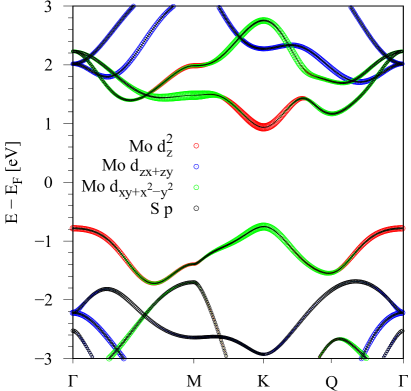
The wave functions we use for the Hamiltonian are and , corresponding to the conduction band (CB) and the valence band (VB) at K and K’, since the band edges are formed by different -orbitals from the transition metal, see Fig. 1, in agreement with literature Kormányos et al. (2015). The model Hamiltonian to describe the band structure (including SOC) of the TMDC close to K () and K’ () is
| (1) | ||||
| (2) | ||||
| (3) | ||||
| (4) |
Here, is the Fermi velocity and the Cartesian components and of the electron wave vector are measured from K (K’). The pseudospin Pauli matrices are acting on the (CB,VB) subspace and spin Pauli matrices are acting on the () subspace, with . For shorter notation we introduce . TMDCs are semiconductors, and thus introduces a gap, represented by parameter , in the band structure such that describes a gapped spectrum with spin-degenerate parabolic CB and VB. In addition the bands are spin-split due to SOC which is captured by the term with the parameters and describing the spin splitting of the CB and VB. The Hamiltonian is already suitable to describe the spectrum of bare TMDCs around the band edges at K and K’. The four basis states are , , , and . From now on, we consider only first-principles results, where SOC is included.
III Geometry, Band Structure, and Fitted results
To study proximity effects in TMDCs, one has to interface them with other materials, for example CrI3 to get proximity exchange Zollner et al. (2019). In these heterostructures, usually lattice mismatch between the constituents is present, and we have to find a common unit cell for them, to be applicable to periodic DFT calculations. The usual approach is to create supercells of the individual materials, such that they can form a common unit cell, and strain is minimized. Therefore, we introduce biaxial strain on the TMDC lattice, up to a reasonable limit, in heterostructure calculations. An important question is, whether the biaxial strain, will influence the intrinsic properties, such as orbital gap and spin-orbit splittings, of the TMDC. Therefore, we calculate the band structures of the monolayer TMDCs in a unit cell for different lattice constants, corresponding to biaxial strain with a maximum of .
The electronic structure calculations and structural relaxation of our geometries are performed with density functional theory (DFT) Hohenberg and Kohn (1964) using Quantum Espresso Giannozzi et al. (2009). Self-consistent calculations are performed with the -point sampling of for bare TMDC monolayers. We use an energy cutoff for charge density of Ry, and the kinetic energy cutoff for wavefunctions is Ry for the scalar relativistic pseudopotential with the projector augmented wave method Kresse and Joubert (1999) with the Perdew-Burke-Ernzerhof (PBE) exchange correlation functional Perdew et al. (1996). When SOC is included, the fully relativistic versions of the pseudopotentials are used. In order to simulate quasi-2D systems, a vacuum of at least Å is used to avoid interactions between periodic images in our slab geometries. Structural relaxations of the monolayers, are performed with a quasi-Newton algorithm based on the trust radius procedure, until all components of all forces are reduced below [Ry/], where is the Bohr radius.
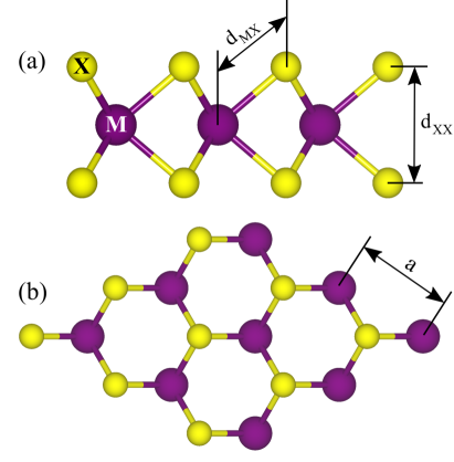
In Fig. 2 we show the geometry of a TMDC monolayer with general structure MX2, where M is the transition metal (Mo, W) and X is the chalcogen atom (S, Se). The distance between two chalcogen atoms is , the distance between the transition metal and the chalcogen atom is , and the distance between two transition metal atoms is the lattice constant . We consider a series of lattice constants, close to the experimental and theoretically predicted values of each TMDC, as summarized in Table 1.
| MoS2 | WS2 | MoSe2 | WSe2 | |
|---|---|---|---|---|
| (exp.) [Å] | 3.15 | 3.153 | 3.288 | 3.282 |
| (calc.) [Å] | 3.185 | 3.18 | 3.319 | 3.319 |
| (calc.) [Å] | 2.417 | 2.417 | 2.547 | 2.550 |
| (calc.) [Å] | 3.138 | 3.145 | 3.357 | 3.364 |
| [eV] | 1.687 | 1.812 | 1.461 | 1.525 |
| [] | 5.338 | 6.735 | 4.597 | 5.948 |
| [meV] | -1.41 | 15.72 | -10.45 | 19.86 |
| [meV] | 74.6 | 213.46 | 93.25 | 233.07 |

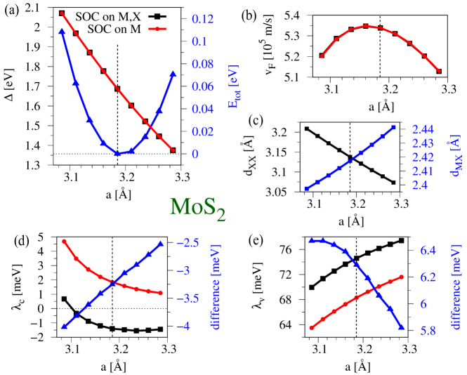
The calculated band structure of MoS2 including SOC is shown in Fig. 3 as a representative example for all considered TMDCs. In agreement with previous calculations Kormányos et al. (2014); Liu et al. (2015); Kośmider et al. (2013); Kormányos et al. (2015), we observe the spin valley coupling at K and K’ point. We are able to fit the Hamiltonian, , to the low energy bands of the TMDC at K and K’ valley and obtain a very good agreement with the calculated band structure, as can be seen in Figs. 3(b,c). The fit parameters for the different TMDCs are summarized in Table 1, considering the equilibrium lattice constants obtained from first-principles lattice relaxation.
In order to analyze the dependence on the lattice constant, i. e., biaxial strain, we allow the chalcogen atoms to relax in their position, for every considered lattice constant. Therefore, we do not change the symmetry, but naturally the distances and will change, as we apply biaxial strain. We then calculate the low energy band structure around the K and K’ valleys and fit the model Hamiltonian , for a series of lattice constants. Due to time-reversal symmetry, it is enough to fit the Hamiltonian around the K point, taking into account the spin expectation values of the bands in order to find the correct signs of and . The three parameters , , and are fitted at the K point, where we have four DFT-energies and three energy differences. The remaining parameter is fitted around the K point, to capture the curvature of the bands. The fitted parameters are thus free from correlations. In Fig. 4 we show the fit parameters obtained for MoS2 as function of the lattice constant. We find that the total energy E is minimized for the DFT predicted lattice constant Kormányos et al. (2015), which slightly deviate from the experimentally determined one for a bulk TMDC, also listed in Table 1.
As we vary the lattice constant from smaller to larger values the distance between two chalcogen atoms is getting smaller, while the distance between the transiton metal atom and the chalcogen atom is getting larger, see Fig. 4(c). The parameter , describing the orbital gap at K and K’ valley, decreases as we increase the lattice constant in agreement with literature Chang et al. (2013); Wang et al. (2014); Frisenda et al. (2017); Johari and Shenoy (2012); Muoi et al. (2019); Ahn et al. (2017). Keeping the orbital decomposed band structure (Fig. 1) in mind, the lattice constant influences all atomic distances, the overlap of and -orbitals, and matrix elements in a tight-binding model perspective Cappelluti et al. (2013); Liu et al. (2013). Consequently, the energy of a given band at a certain -point changes with the atomic distances. For example, the CB (VB) edge at the K () point is formed by -orbitals and shifts down (up) in energy with increasing lattice constant, see animations in the Supplemental Material 111See Supplemental Material at [URL will be inserted by publisher] including Refs. Perdew et al. (2008, 1996), where we show band structure animations, further fit results for WS2, WSe2, and MoSe2 as function of the lattice constant, and a comparison between PBE and PBEsol functional for all TMDCs..
Note that for MoS2 and strains of about % (+1%), when we have a smaller (larger) lattice constant, the band gap becomes indirect Muoi et al. (2019); Johari and Shenoy (2012); Wang et al. (2014) and is at K Q ( K), where Q is the CB side valley along the K- line, see Fig. 1. For the other TMDCs, the situation is similar, but for different strain amplitudes. Tuning the gap with uniaxial or biaxial strain consequently modifies the optical properties, such as the photolominescence spectrum, exciton-phonon coupling and circular dichroism Niehues et al. (2018); Feierabend et al. (2017); Aslan et al. (2018a); Aas and Bulutay (2018). It has also been shown that strain applied to MoS2-based photodetectors can control the response time of the devices Gant et al. (2019). We address the effects of strain in the direct-indirect optical transitions in Sec. IV.1 and the role of excitonic effects in the direct gap regime in Sec. IV.2.
| MoS2 | MoSe2 | |||||||||
|---|---|---|---|---|---|---|---|---|---|---|
| 3.0854 | 2.071 | 5.205 | 0.666 | 69.95 | 3.219 | 1.779 | 4.429 | -9.120 | 89.10 | |
| 3.1104 | 1.969 | 5.287 | -0.336 | 71.34 | 3.244 | 1.696 | 4.507 | -10.22 | 90.39 | |
| 3.1354 | 1.871 | 5.331 | -0.887 | 72.54 | 3.269 | 1.615 | 4.560 | -10.59 | 91.54 | |
| 3.1604 | 1.777 | 5.347 | -1.207 | 73.64 | 3.294 | 1.536 | 4.587 | -10.64 | 92.50 | |
| 3.1854 | 1.687 | 5.338 | -1.410 | 74.60 | 3.319 | 1.461 | 4.597 | -10.45 | 93.25 | |
| 3.2104 | 1.602 | 5.310 | -1.479 | 75.43 | 3.344 | 1.389 | 4.589 | -10.15 | 93.95 | |
| 3.2354 | 1.522 | 5.263 | -1.550 | 76.16 | 3.369 | 1.320 | 4.564 | -9.760 | 94.42 | |
| 3.2604 | 1.446 | 5.202 | -1.518 | 76.82 | 3.394 | 1.255 | 4.526 | -9.309 | 94.78 | |
| 3.2854 | 1.375 | 5.128 | -1.450 | 77.42 | 3.419 | 1.194 | 4.480 | -8.780 | 94.98 | |
| WS2 | WSe2 | |||||||||
| 3.080 | 2.274 | 6.752 | 43.08 | 191.46 | 3.219 | 1.917 | 5.964 | 51.18 | 212.16 | |
| 3.105 | 2.153 | 6.815 | 31.80 | 197.68 | 3.244 | 1.816 | 6.011 | 38.40 | 218.12 | |
| 3.130 | 2.035 | 6.820 | 24.40 | 203.40 | 3.269 | 1.716 | 6.019 | 29.87 | 223.60 | |
| 3.155 | 1.921 | 6.795 | 19.35 | 208.64 | 3.294 | 1.619 | 5.995 | 24.00 | 228.56 | |
| 3.180 | 1.812 | 6.735 | 15.72 | 213.46 | 3.319 | 1.525 | 5.948 | 19.86 | 233.07 | |
| 3.205 | 1.710 | 6.655 | 13.07 | 217.83 | 3.344 | 1.437 | 5.881 | 16.85 | 237.10 | |
| 3.230 | 1.614 | 6.542 | 11.11 | 221.81 | 3.369 | 1.353 | 5.798 | 14.63 | 240.72 | |
| 3.255 | 1.526 | 6.437 | 9.62 | 225.37 | 3.394 | 1.276 | 5.702 | 13.02 | 243.86 | |
| 3.280 | 1.443 | 6.311 | 8.46 | 228.57 | 3.419 | 1.203 | 5.596 | 11.81 | 246.58 | |
The Fermi velocity, , reflecting the effective mass, does not change drastically as we vary the lattice constant, but still we see some characteristic nonlinear behavior, see Fig. 4(b). The reason is that Xiao et al. (2012), given by the effective hopping integral between and orbitals, mediated by chalcogen orbitals, is influenced by atomic distances and . The most interesting are the SOC parameters and , see Figs. 4(d,e). Because we have two different atomic species in the unit cell, we consider the influence of the individual atoms, M and X, on the SOC parameters, which represent the spin-splittings of the CB and VB. For that we calculate the band structure once with SOC on both atom species and once artificially turning off SOC on the chalcogen atom, by using a non-relativistic pseudopotential for it. This allows us to resolve the contributions from the M and X atom to the SOC parameters individually. The difference (blue curve) reflects the contribution from the chalcogen atoms to the splittings, see Figs. 4(d,e).
We find that the parameter decreases, while the parameter increases with increasing lattice constant. Both parameters depend in a nonlinear fashion on the biaxial strain. At a certain lattice constant, the CB splitting in MoS2 can even make a transition through zero, reordering the two spin-split bands in Fig. 3(b). In addition, the differences (blue curve) in and decrease in magnitude, as we increase the lattice constant. This we can understand from the fact, that the spin-splittings of the CB and VB result from an interplay of the atomic SOC values of the transition-metal and chalcogen atoms, as derived from perturbation theory in Ref. Kośmider et al. (2013). We confirm that the chalcogen atom has a negative contribution to the CB splitting and a positive contribution to the VB splitting, while the transition metal atom gives positive contributions to both splittings, in agreement with Ref. Kośmider et al. (2013). In Fig. 4 we explicitly show, how the spin splittings depend on the lattice constant and how the different atom types contribute to it for the case of MoS2. What is still missing so far, is a microscopic orbital-based description of how the spin splittings depend on the lattice constant and respective distances, as for example derived for graphene Konschuh et al. (2010).
In a fashion similar to Fig. 4 we calculate the same dependence on the lattice constant for other TMDCs, see Supplemental Material 111See Supplemental Material at [URL will be inserted by publisher] including Refs. Perdew et al. (2008, 1996), where we show band structure animations, further fit results for WS2, WSe2, and MoSe2 as function of the lattice constant, and a comparison between PBE and PBEsol functional for all TMDCs.. For all of them, we can observe similar characteristic trends of the parameters, varying as function of the lattice constant. The fitted parameters as a function of the lattice constant are summarized in Table 2 for all TMDCs. An interesting observation is that the CB SOC parameter for Mo-based systems is opposite in sign compared to W-based materials, as already pointed out in earlier works Kormányos et al. (2015, 2014); Kośmider et al. (2013).
In the Supplemental Material 111See Supplemental Material at [URL will be inserted by publisher] including Refs. Perdew et al. (2008, 1996), where we show band structure animations, further fit results for WS2, WSe2, and MoSe2 as function of the lattice constant, and a comparison between PBE and PBEsol functional for all TMDCs. we provide animations that explicitly show the evolution of the TMDC band structures as function of biaxial strain. Additionally, we compare the results for all TMDCs obtained from two different exchange correlation functionals, namely PBE Perdew et al. (1996) and PBEsol Perdew et al. (2008). In the case of PBEsol, which improves equilibrium properties, the total energy is minimized for the experimental lattice constant. However, the overall magnitudes and trends of the parameters as function of the lattice constant, are barely different. We conclude that the PBEsol functional should hardly influence the following results on exciton energy levels and gauge factors, and results can be compared to experiment, when regarding them relative to 0% strain (equilibrium lattice constant).
IV Strain tunable optical transitions
IV.1 Direct and indirect band gap regimes
In the previous section we analyzed the strain effects in the band structure of MoS2 and found that different strain regimes induce a direct to indirect band gap transition. This feature is also present in the other TMDCs we investigated (see Supplemental Material 111See Supplemental Material at [URL will be inserted by publisher] including Refs. Perdew et al. (2008, 1996), where we show band structure animations, further fit results for WS2, WSe2, and MoSe2 as function of the lattice constant, and a comparison between PBE and PBEsol functional for all TMDCs.). In order to obtain a deeper insight into this direct to indirect band gap switching, in this section we discuss the strain dependence of the single-particle optical transitions for all the TMDCs. We focus on the mostly affected optical transitions, depicted in Fig. 5(a) for MoS2. The evolution of these transitions with respect to applied strain is shown in Fig. 5(b-e) for MoS2, MoSe2, WS2 and WSe2, respectively. The overall trend is similar for all TMDCs: negative strain induces indirect band gap for the K-Q transition while positive strain values cause the -K transition to have the smallest energy. For MoSe2 and WSe2 the amount of positive strain required to reach the -K indirect band gap regime would be larger than the region we investigated here. Additionally, K-Q transitions show a positive slope while K-K and -K show a negative slope. Although a proper comparison to uniaxial strain results may seem unfair due to the different lattice symmetries, it is still worth mentioning that -K transitions have a steeper dependence than the K-K transitions, as observed experimentally for MoS2 Conley et al. (2013) and WS2 Blundo et al. (2019), for instance. Furthermore, theoretical studies based on first-principles calculations have shown such dependencies not only due to uniaxial strain but also in the biaxial strain case Peelaers and Van de Walle (2012); Wang et al. (2014).
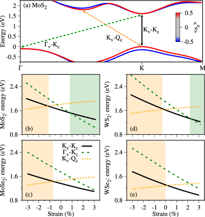
One important figure of merit to analyze the strain dependence is the so called gauge factor of the transition energies, i. e., the rate of energy shift due to the applied strain, typically given in meV/%. In Table 3, we quantify the gauge factors for the different transition energies shown in Figs. 5(b-e). Although these energy transitions do not behave completely linear under strain, we assumed for simplicity a linear behavior throughout the whole strain range we considered. We found that the strength of gauge factors for the indirect -K transitions is nearly twice as large as the direct K-K transitions. On the other hand, the strength of the gauge factors of the indirect K-Q transitions are nearly 2 (4) times smaller than the direct K-K transitions for Mo(W)-based TMDCs. Such large differences in the gauge factors provide important information to identify the evolution of the optical spectra under applied strain.
| MoS2 | MoSe2 | WS2 | WSe2 | |
|---|---|---|---|---|
| K-K | -112.3 | -98.2 | -133.5 | -118.8 |
| -K | -239.9 | -210.2 | -254.0 | -213.4 |
| K-Q | 44.3 | 45.7 | 37.0 | 32.8 |
IV.2 Excitonic effects in the direct band gap regime
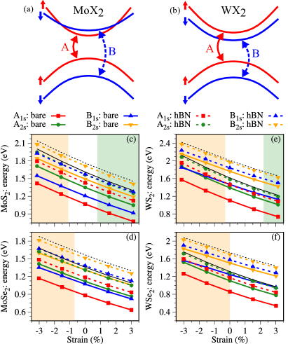
For moderate applied strain the direct band gap at the K point remains the fundamental transition energy. In this section we investigate the role of excitonic effects to such direct transitions under the applied biaxial strain. In a simple picture, an exciton is a quasi-particle created due to the electrostatic Coulomb interaction between electrons and holes Chuang (1995); Haug and Koch (2009). Because of the weak screening of 2D materials, excitons have large binding energies and, therefore, excitonic effects dominate the optical spectra Mak et al. (2010); Chernikov et al. (2014); Qiu et al. (2013); Wang et al. (2018b). Starting from the effective Hamiltonian given in Eq. (1) and fitted parameters given in Table 2, we compute the excitonic spectra of the strained monolayer TMDCs for different bright excitonic states (the s-like excitons) that can be directly probed in experiments. We use the effective Bethe-Salpeter equation (BSE) Rohlfing and Louie (2000); Scharf et al. (2017, 2019); Tedeschi et al. (2019b); Faria Junior et al. (2019); Zollner et al. (2019) with the electron-hole interaction mediated by the Rytova-Keldysh potential Rytova (1967); Keldysh (1979); Cudazzo et al. (2011); Berkelbach et al. (2013). The screening lengths of the TMDCs are taken from the study of Berkelbach et al. Berkelbach et al. (2013). The BSE is solved on a 2D -grid from -0.5 to 0.5 in the and directions with total discretization of points (leading to a spacing of ). To improve convergence, the Coulomb potential is averaged around each -point in a square region of to discretized with points Scharf et al. (2017); Zollner et al. (2019).
We focus on two different exciton types: the so-called A and B excitons. In Mo(W)-based TMDCs, the A excitons are formed by the first VB and first (second) CB while B excitons are formed by the second VB and second (first) CB, sketched in Figs. 6(a-b). In Figs. 6(c-f) we show the behavior of the total energy of A and B excitons as a function of the applied biaxial strain in two different dielectric environments: bare (effective dielectric constant of ) and hexagonal boron nitride (hBN) encapsulated TMDCs (effective dielectric constant of Stier et al. (2018)). The subindices 1s and 2s indicate the first and second s-like exciton states, respectively. Despite the nonlinear behavior of , and seen in Fig. 4, the A excitons evolve in quite a linear fashion with the same qualitative behavior for all TMDCs. On the other hand, the B excitons show a different behavior for Mo and W-based TMDCs as function of strain. For the bare case, in Mo-based TMDCs the B exciton would be the second visible absorption peak while in W-based TMDCs additional peaks of the A excitons would be visible at energies lower than the peaks of the B excitons. Once we change the dielectric environment from bare to hBN-encapsulated, the ordering of the excitonic peaks changes in MoS and MoSe; that is, the B exciton is no longer the second visible peak. Nevertheless, the same qualitative behavior as function of the biaxial strain holds, as discussed for the bare TMDCs case.
| MoS2 | MoSe2 | WS2 | WSe2 | |
| This work | ||||
| E | -112.5 | -98.6 | -144.0 | -131.2 |
| E | -109.8 | -97.2 | -123.8 | -109.7 |
| A: bare | -103.3 | -89.6 | -134.1 | -121.1 |
| A: bare | -106.2 | -92.0 | -137.8 | -124.7 |
| B: bare | -101.7 | -89.5 | -118.1 | -104.4 |
| B: bare | -104.1 | -91.5 | -120.2 | -106.2 |
| A: hBN | -106.9 | -92.7 | -138.6 | -125.5 |
| A: hBN | -110.4 | -96.1 | -142.3 | -129.3 |
| B: hBN | -104.8 | -92.0 | -120.6 | -106.5 |
| B: hBN | -107.9 | -95.0 | -122.7 | -108.6 |
| GW-BSEFrisenda et al. (2017) | ||||
| E | -134 | -115 | -156 | -141 |
| A: bare | -110 | -90 | -151 | -134 |
| B: bare | -107 | -89 | -130 | -111 |
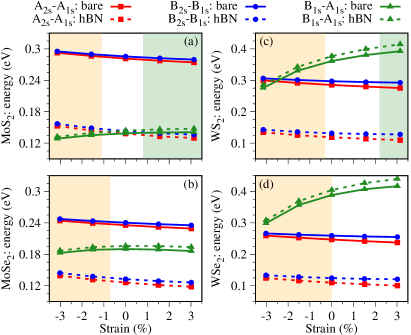
In Table 4, we present the gauge factors for the exciton peaks, i. e., the total energy given in Fig. 6(c-f), extracted as a linear fit in the % to % strain range. As a general trend, the strength of the gauge factors follow the order MoSe MoS WSe WS, and the effect of changing the dielectric surroundings modifies only 2 – 4 meV/%, which can be at the scale of experimental uncertainty. Although we have not taken into account corrections to the band gap, our calculated exciton behaviors are in good agreement with GW-BSE ab-initio calculations from Frisenda et al. Frisenda et al. (2017), also shown in Table 4 for comparison to our results. From the experimental perspective, the amount of studies on biaxial strain is still very scarce and mainly limited to MoS. For the available gauge factors in MoS, Plechinger et al. Plechinger et al. (2015) found -105 meV/% for the A exciton, Lloyd et al. Lloyd et al. (2016) -99 6 meV/% for both A and B excitons and Gant et al. Gant et al. (2019) a value of -94 meV/% for the A exciton. Furthermore, the study of Frisenda et al. Frisenda et al. (2017) also determined experimentally the gauge factor of MoSe, MoS, WSe and WS but the values are smaller than the theoretical results, most likely because the strain present in the substrate is not fully transferred to the TMDC and the calibration is not a straightforward task, as already discussed by the authors Frisenda et al. (2017).
| MoS2 | MoSe2 | WS2 | WSe2 | |
|---|---|---|---|---|
| E-E | 2.7 | 1.4 | 20.2 | 21.5 |
| A-A: bare | -2.9 | -2.5 | -3.7 | -3.6 |
| A-A: hBN | -3.5 | -3.4 | -3.7 | -3.9 |
| B-B: bare | -2.5 | -2.0 | -2.1 | -1.8 |
| B-B: hBN | -3.1 | -2.9 | -2.1 | -2.1 |
| B-A: bare | 1.6 | 0.1 | 16.0 | 16.7 |
| B-A: hBN | 2.1 | 0.7 | 18.0 | 18.9 |
Besides the total exciton energies, it is also helpful to look at how the energy separation of different excitonic levels change under the applied strain. These behaviors are summarized in Fig. 7 for all TMDCs considered here and the corresponding gauge factors are presented in Table 5. Although the change in the dielectric environment has a minor effect on the gauge factors (2 meV/% or less), it drastically changes the total energy difference by hundreds of meV for the A-A and B-B exciton separation (compare solid and dashed lines with squares and circles in Fig. 7). On the other hand the energy separation of B-A excitons is affected by only a few or tens of meV (compare solid and dashed lines with triangles in Fig. 7). Furthermore, the gauge factor of B-A energy difference for W-based compounds is one order of magnitude larger than that of the Mo-based compounds, reflecting the larger increase of (see for instance Fig. 4). We point out that for WSe2 our calculations reveal the same qualitative trends as in recent experiments with uniaxial strain by Aslan et al. Aslan et al. (2018a), in which they found a gauge factor of -61 meV/% for the A-A exciton separation and 10 meV/% for B-A exciton separation.
V Summary
We have shown that applying biaxial strain to monolayer TMDCs induces drastic changes in their orbital, spin-orbit and, consequently, optical properties. Furthermore, we showed on a quantitative level, how the spin-orbit band splittings in a TMDC depend on biaxial strain and on the SOC contributions from the individual atoms. Additionally, by employing the Bethe-Salpeter equation combined with a minimal tight-binding Hamiltonian fitted to the ab-initio band structure, we have calculated the evolution of several direct exciton peaks as a function of biaxial strain and for different dielectric surroundings. Specifically, we found that the gauge factors are slightly affected by the dielectric environment and are mainly ruled by the atomic composition, with the ordering MoSe MoS WSe WS. Our results provide valuable insights into how strain can modify the TMDC properties within van der Waals heterostructures, and the parameter sets we provided can be applied to investigate other physical phenomena.
Acknowledgements.
We thank A. Polimeni for helpful discussions. This work was supported by DFG SPP 1666, DFG SFB 1277 (project B05), the European Unions Horizon 2020 research and innovation program under Grant No. 785219, the Alexander von Humboldt Foundation and Capes (Grant No. 99999.000420/2016-06).References
- Kormányos et al. (2015) A. Kormányos, G. Burkard, M. Gmitra, J. Fabian, V. Zólyomi, N. D. Drummond, and V. Fal’ko, 2D Materials 2, 022001 (2015).
- Liu et al. (2015) G.-B. Liu, D. Xiao, Y. Yao, X. Xu, and W. Yao, Chem. Soc. Rev. 44, 2643 (2015).
- Tonndorf et al. (2013) P. Tonndorf, R. Schmidt, P. Böttger, X. Zhang, J. Börner, A. Liebig, M. Albrecht, C. Kloc, O. Gordan, D. R. T. Zahn, S. Michaelis de Vasconcellos, and R. Bratschitsch, Opt. Express 21, 4908 (2013).
- Tongay et al. (2012) S. Tongay, J. Zhou, C. Ataca, K. Lo, T. S. Matthews, J. Li, J. C. Grossman, and J. Wu, Nano Lett. 12, 5576 (2012).
- Eda et al. (2011) G. Eda, H. Yamaguchi, D. Voiry, T. Fujita, M. Chen, and M. Chhowalla, Nano Lett. 11, 5111 (2011).
- Li and Yang (2014) X. Li and J. Yang, J. Mater. Chem. C 2, 7071 (2014).
- Carteaux et al. (1995) V. Carteaux, D. Brunet, G. Ouvrard, and G. Andre, J. Phys.: Condens. Mat. 7, 69 (1995).
- Gong et al. (2017) C. Gong, L. Li, Z. Li, H. Ji, A. Stern, Y. Xia, T. Cao, W. Bao, C. Wang, Y. Wang, Z. Q. Qiu, R. J. Cava, S. G. Louie, J. Xia, and X. Zhang, Nature 546, 265 (2017).
- Siberchicot et al. (1996) B. Siberchicot, S. Jobic, V. Carteaux, P. Gressier, and G. Ouvrard, J. Phys. Chem. 100, 5863 (1996).
- Lin et al. (2017) G. T. Lin, H. L. Zhuang, X. Luo, B. J. Liu, F. C. Chen, J. Yan, Y. Sun, J. Zhou, W. J. Lu, P. Tong, Z. G. Sheng, Z. Qu, W. H. Song, X. B. Zhu, and Y. P. Sun, Phys. Rev. B 95, 245212 (2017).
- Wang et al. (2018a) Z. Wang, T. Zhang, M. Ding, B. Dong, Y. Li, M. Chen, X. Li, J. Huang, H. Wang, X. Zhao, Y. Li, D. Li, C. Jia, L. Sun, H. Guo, Y. Ye, D. Sun, Y. Chen, T. Yang, J. Zhang, S. Ono, Z. Han, and Z. Zhang, Nat. Nanotechnol. 13, 554 (2018a).
- Liu et al. (2016) J. Liu, Q. Sun, Y. Kawazoe, and P. Jena, Phys. Chem. Chem. Phys. 18, 8777 (2016).
- Zhang et al. (2015) W.-B. Zhang, Q. Qu, P. Zhu, and C.-H. Lam, J. Mater. Chem. C 3, 12457 (2015).
- McGuire et al. (2015) M. A. McGuire, H. Dixit, V. R. Cooper, and B. C. Sales, Chemistry of Materials 27, 612 (2015).
- Webster et al. (2018) L. Webster, L. Liang, and J. A. Yan, Phys. Chem. Chem. Phys. 20, 23546 (2018).
- Huang et al. (2017) B. Huang, G. Clark, E. Navarro-Moratalla, D. R. Klein, R. Cheng, K. L. Seyler, D. Zhong, E. Schmidgall, M. A. McGuire, D. H. Cobden, W. Yao, D. Xiao, P. Jarillo-Herrero, and X. Xu, Nature 546, 270 (2017).
- Jiang et al. (2018a) P. Jiang, L. Li, Z. Liao, Y. Zhao, and Z. Zhong, Nano Letters 18, 3844 (2018a).
- Soriano et al. (2019) D. Soriano, C. Cardoso, and J. Fernández-Rossier, Solid State Communications 299, 113662 (2019).
- Huang et al. (2018) B. Huang, G. Clark, D. R. Klein, D. MacNeill, E. Navarro-Moratalla, K. L. Seyler, N. Wilson, M. A. McGuire, D. H. Cobden, D. Xiao, W. Yao, P. Jarillo-Herrero, and X. Xu, Nature Nanotechnology 13, 544 (2018).
- Jiang et al. (2018b) S. Jiang, L. Li, Z. Wang, K. F. Mak, and J. Shan, Nat. Nanotechnol. 13, 549 (2018b).
- Wu et al. (2019) M. Wu, Z. Li, T. Cao, and S. G. Louie, Nat. Commun. 10, 1 (2019).
- Yoshida et al. (2016) M. Yoshida, J. Ye, T. Nishizaki, N. Kobayashi, and Y. Iwasa, Appl. Phys. Lett. 108, 202602 (2016).
- Noat et al. (2015) Y. Noat, J. A. Silva-Guillén, T. Cren, V. Cherkez, C. Brun, S. Pons, F. Debontridder, D. Roditchev, W. Sacks, L. Cario, P. Ordejón, A. García, and E. Canadell, Phys. Rev. B 92, 134510 (2015).
- Zhu et al. (2016) X. Zhu, Y. Guo, H. Cheng, J. Dai, X. An, J. Zhao, K. Tian, S. Wei, X. Cheng Zeng, C. Wu, and Y. Xie, Nat. Commun. 7, 11210 (2016).
- Xu et al. (2018) S.-Y. Xu, Q. Ma, H. Shen, V. Fatemi, S. Wu, T.-R. Chang, G. Chang, A. M. M. Valdivia, C.-K. Chan, Q. D. Gibson, J. Zhou, Z. Liu, K. Watanabe, T. Taniguchi, H. Lin, R. J. Cava, L. Fu, N. Gedik, and P. Jarillo-Herrero, Nature Physics 14, 900 (2018).
- Fabian et al. (2007) J. Fabian, A. Matos-Abiague, C. Ertler, P. Stano, and I. Žutić, Acta Phys. Slov. 57, 342 (2007).
- Žutić et al. (2004) I. Žutić, J. Fabian, and S. Das Sarma, Rev. Mod. Phys. 76, 323 (2004).
- Mak et al. (2010) K. F. Mak, C. Lee, J. Hone, J. Shan, and T. F. Heinz, Phys. Rev. Lett. 105, 136805 (2010).
- Chernikov et al. (2014) A. Chernikov, T. C. Berkelbach, H. M. Hill, A. Rigosi, Y. Li, O. B. Aslan, D. R. Reichman, M. S. Hybertsen, and T. F. Heinz, Phys. Rev. Lett. 113, 076802 (2014).
- Gibertini et al. (2014) M. Gibertini, F. M. D. Pellegrino, N. Marzari, and M. Polini, Phys. Rev. B 90, 245411 (2014).
- Wang et al. (2018b) G. Wang, A. Chernikov, M. M. Glazov, T. F. Heinz, X. Marie, T. Amand, and B. Urbaszek, Rev. Mod. Phys. 90, 021001 (2018b).
- Wang et al. (2012) Q. H. Wang, K. Kalantar-Zadeh, A. Kis, J. N. Coleman, and M. S. Strano, Nat. Nanotechnol. 7, 699 (2012), 1205.1822 .
- Gmitra and Fabian (2015) M. Gmitra and J. Fabian, Phys. Rev. B 92, 155403 (2015).
- Luo et al. (2017) Y. K. Luo, J. Xu, T. Zhu, G. Wu, E. J. McCormick, W. Zhan, M. R. Neupane, and R. K. Kawakami, Nano Lett. 17, 3877 (2017).
- Avsar et al. (2017) A. Avsar, D. Unuchek, J. Liu, O. L. Sanchez, K. Watanabe, T. Taniguchi, B. Özyilmaz, and A. Kis, ACS Nano 11, 11678 (2017).
- Schaibley et al. (2016) J. R. Schaibley, H. Yu, G. Clark, P. Rivera, J. S. Ross, K. L. Seyler, W. Yao, and X. Xu, Nature Reviews Materials 1, 16055 (2016).
- Langer et al. (2018) F. Langer, C. P. Schmid, S. Schlauderer, M. Gmitra, J. Fabian, P. Nagler, C. Schüller, T. Korn, P. G. Hawkins, J. T. Steiner, U. Huttner, S. W. Koch, M. Kira, and R. Huber, Nature 557, 76 (2018).
- Zhong et al. (2017) D. Zhong, K. L. Seyler, X. Linpeng, R. Cheng, N. Sivadas, B. Huang, E. Schmidgall, T. Taniguchi, K. Watanabe, M. A. McGuire, W. Yao, D. Xiao, K.-M. C. Fu, and X. Xu, Science Advances 3, e1603113 (2017).
- Xiao et al. (2012) D. Xiao, G.-B. Liu, W. Feng, X. Xu, and W. Yao, Phys. Rev. Lett. 108, 196802 (2012).
- He et al. (2013) K. He, C. Poole, K. F. Mak, and J. Shan, Nano Lett. 13, 2931 (2013).
- Conley et al. (2013) H. J. Conley, B. Wang, J. I. Ziegler, R. F. Haglund, S. T. Pantelides, and K. I. Bolotin, Nano Lett. 13, 3626 (2013).
- Plechinger et al. (2015) G. Plechinger, A. Castellanos-Gomez, M. Buscema, H. S. van der Zant, G. A. Steele, A. Kuc, T. Heine, C. Schueller, and T. Korn, 2D Materials 2, 015006 (2015).
- Ji et al. (2016) J. Ji, A. Zhang, T. Xia, P. Gao, Y. Jie, Q. Zhang, and Q. Zhang, Chinese Phys. B 25, 077802 (2016).
- Schmidt et al. (2016) R. Schmidt, I. Niehues, R. Schneider, M. Drüppel, T. Deilmann, M. Rohlfing, S. Vasconcellos, A. Castellanos-Gomez, and R. Bratschitsch, 2D Mater. 3, 21011 (2016).
- Lloyd et al. (2016) D. Lloyd, X. Liu, J. W. Christopher, L. Cantley, A. Wadehra, B. L. Kim, B. B. Goldberg, A. K. Swan, and J. S. Bunch, Nano Lett. 16, 5836 (2016).
- Aslan et al. (2018a) O. B. Aslan, M. Deng, and T. F. Heinz, Phys. Rev. B 98, 115308 (2018a).
- Aslan et al. (2018b) O. B. Aslan, I. M. Datye, M. J. Mleczko, K. Sze Cheung, S. Krylyuk, A. Bruma, I. Kalish, A. V. Davydov, E. Pop, and T. F. Heinz, Nano Lett. 18, 2485 (2018b).
- Frisenda et al. (2017) R. Frisenda, M. Drüppel, R. Schmidt, S. Michaelis de Vasconcellos, D. Perez de Lara, R. Bratschitsch, M. Rohlfing, and A. Castellanos-Gomez, npj 2D Mater. Appl. 1, 10 (2017).
- Gant et al. (2019) P. Gant, P. Huang, D. P. de Lara, D. Guo, R. Frisenda, and A. Castellanos-Gomez, Materials Today 27, 8 (2019).
- Tedeschi et al. (2019a) D. Tedeschi, E. Blundo, M. Felici, G. Pettinari, B. Liu, T. Yildrim, E. Petroni, C. Zhang, Y. Zhu, S. Sennato, Y. Lu, and A. Polimeni, Advanced Materials 31, 1903795 (2019a).
- Iff et al. (2019) O. Iff, D. Tedeschi, J. Martín-Sánchez, M. Moczała-Dusanowska, S. Tongay, K. Yumigeta, J. Taboada-Gutiérrez, M. Savaresi, A. Rastelli, P. Alonso-González, S. Höfling, R. Trotta, and C. Schneider, Nano Letters 19, 6931 (2019).
- Blundo et al. (2019) E. Blundo, M. Felici, T. Yildirim, G. Pettinari, D. Tedeschi, A. Miriametro, B. Liu, W. Ma, Y. Lu, and A. Polimeni, (2019), 1910.11847 .
- Peelaers and Van de Walle (2012) H. Peelaers and C. G. Van de Walle, Phys. Rev. B 86, 241401 (2012).
- Johari and Shenoy (2012) P. Johari and V. B. Shenoy, ACS Nano 6, 5449 (2012).
- Castellanos-Gomez et al. (2013) A. Castellanos-Gomez, R. Roldán, E. Cappelluti, M. Buscema, F. Guinea, H. S. van der Zant, and G. A. Steele, Nano letters 13, 5361 (2013).
- Kumar et al. (2015) S. Kumar, A. Kaczmarczyk, and B. D. Gerardot, Nano letters 15, 7567 (2015).
- Branny et al. (2016) A. Branny, G. Wang, S. Kumar, C. Robert, B. Lassagne, X. Marie, B. D. Gerardot, and B. Urbaszek, Applied Physics Letters 108, 142101 (2016).
- Proscia et al. (2018) N. V. Proscia, Z. Shotan, H. Jayakumar, P. Reddy, C. Cohen, M. Dollar, A. Alkauskas, M. Doherty, C. A. Meriles, and V. M. Menon, Optica 5, 1128 (2018).
- Novoselov et al. (2016) K. S. Novoselov, A. Mishchenko, A. Carvalho, and A. H. Castro Neto, Science 353, aac9439 (2016).
- Geim and Grigorieva (2013) A. K. Geim and I. V. Grigorieva, Nature 499, 419 (2013), 1307.6718 .
- Žutić et al. (2019) I. Žutić, A. Matos-Abiague, B. Scharf, H. Dery, and K. Belashchenko, Materials Today 22, 85 (2019).
- Gmitra et al. (2016) M. Gmitra, D. Kochan, P. Högl, and J. Fabian, Phys. Rev. B 93, 155104 (2016).
- Zollner et al. (2019) K. Zollner, P. E. Faria Junior, and J. Fabian, Phys. Rev. B 100, 085128 (2019).
- Seyler et al. (2018) K. Seyler, D. Zhong, B. Huang, X. Linpeng, N. P. Wilson, T. Taniguchi, K. Watanabe, W. Yao, D. Xiao, M. A. McGuire, K. M. Fu, and X. Xu, Nano letters 18, 3823 (2018).
- Qi et al. (2015) J. Qi, X. Li, Q. Niu, and J. Feng, Physical Review B 92, 121403 (2015).
- Hohenberg and Kohn (1964) P. Hohenberg and W. Kohn, Phys. Rev. 136, B864 (1964).
- Giannozzi et al. (2009) P. Giannozzi, S. Baroni, N. Bonini, M. Calandra, R. Car, C. Cavazzoni, D. Ceresoli, G. L. Chiarotti, M. Cococcioni, I. Dabo, A. D. Corso, S. Fabris, G. Fratesi, S. de Gironcoli, R. Gebauer, U. Gerstmann, C. Gougoussis, A. Kokalj, M. Lazzeri, L. Martin-Samos, N. Marzari, F. Mauri, R. Mazzarello, S. Paolini, A. Pasquarello, L. Paulatto, C. Sbraccia, S. Scandolo, G. Sclauzero, A. P. Seitsonen, A. Smogunov, P. Umari, and R. M. Wentzcovitch, J. Phys.: Condens. Mat. 21, 395502 (2009).
- Kresse and Joubert (1999) G. Kresse and D. Joubert, Phys. Rev. B 59, 1758 (1999).
- Perdew et al. (1996) J. P. Perdew, K. Burke, and M. Ernzerhof, Phys. Rev. Lett. 77, 3865 (1996).
- Wakabayashi et al. (1975) N. Wakabayashi, H. G. Smith, and R. M. Nicklow, Physical Review B 12, 659 (1975).
- Schutte et al. (1987) W. J. Schutte, J. L. De Boer, and F. Jellinek, Journal of Solid State Chemistry 70, 207 (1987).
- James and Lavik (1963) P. B. James and M. T. Lavik, Acta Crystallographica 16, 1183 (1963).
- Kormányos et al. (2014) A. Kormányos, V. Zólyomi, N. D. Drummond, and G. Burkard, Phys. Rev. X 4, 011034 (2014).
- Kośmider et al. (2013) K. Kośmider, J. W. González, and J. Fernández-Rossier, Phys. Rev. B 88, 245436 (2013).
- Chang et al. (2013) C.-H. Chang, X. Fan, S.-H. Lin, and J.-L. Kuo, Phys. Rev. B 88, 195420 (2013).
- Wang et al. (2014) L. Wang, A. Kutana, and B. I. Yakobson, Annalen der Physik 526, L7 (2014).
- Muoi et al. (2019) D. Muoi, N. N. Hieu, H. T. Phung, H. V. Phuc, B. Amin, B. D. Hoi, N. V. Hieu, L. C. Nhan, C. V. Nguyen, and P. Le, Chemical Physics 519, 69 (2019).
- Ahn et al. (2017) G. H. Ahn, M. Amani, H. Rasool, D.-h. Lien, J. P. Mastandrea, J. W. Ager III, M. Dubey, D. C. Chrzan, A. M. Minor, and A. Javey, Nat. Commun. 8, 608 (2017).
- Cappelluti et al. (2013) E. Cappelluti, R. Roldán, J. A. Silva-Guillén, P. Ordejón, and F. Guinea, Phys. Rev. B 88, 075409 (2013).
- Liu et al. (2013) G.-B. Liu, W.-Y. Shan, Y. Yao, W. Yao, and D. Xiao, Phys. Rev. B 88, 085433 (2013).
- Note (1) See Supplemental Material at [URL will be inserted by publisher] including Refs. Perdew et al. (2008, 1996), where we show band structure animations, further fit results for WS2, WSe2, and MoSe2 as function of the lattice constant, and a comparison between PBE and PBEsol functional for all TMDCs.
- Niehues et al. (2018) I. Niehues, R. Schmidt, M. Drüppel, P. Marauhn, D. Christiansen, M. Selig, G. Berghäuser, D. Wigger, R. Schneider, L. Braasch, R. Koch, A. Castellanos-Gomez, T. Kuhn, A. Knorr, E. Malic, M. Rohlfing, S. Michaelis de Vasconcellos, and R. Bratschitsch, Nano Lett. 18, 1751 (2018).
- Feierabend et al. (2017) M. Feierabend, A. Morlet, G. Berghäuser, and E. Malic, Phys. Rev. B 96, 045425 (2017).
- Aas and Bulutay (2018) S. Aas and C. Bulutay, Opt. Express 26, 28672 (2018).
- Konschuh et al. (2010) S. Konschuh, M. Gmitra, and J. Fabian, Physical Review B 82, 245412 (2010).
- Perdew et al. (2008) J. P. Perdew, A. Ruzsinszky, G. I. Csonka, O. A. Vydrov, G. E. Scuseria, L. A. Constantin, X. Zhou, and K. Burke, Phys. Rev. Lett. 100, 136406 (2008).
- Chuang (1995) S. L. Chuang, Physics of optoelectronic devices (John Wiley, New York, 1995).
- Haug and Koch (2009) H. Haug and S. W. Koch, Quantum Theory of the Optical and Electronic Properties of Semiconductors: Fifth Edition (World Scientific Publishing Company, 2009).
- Qiu et al. (2013) D. Y. Qiu, F. H. da Jornada, and S. G. Louie, Phys. Rev. Lett. 111, 216805 (2013).
- Rohlfing and Louie (2000) M. Rohlfing and S. G. Louie, Phys. Rev. B 62, 4927 (2000).
- Scharf et al. (2017) B. Scharf, G. Xu, A. Matos-Abiague, and I. Žutić, Phys. Rev. Lett. 119, 127403 (2017).
- Scharf et al. (2019) B. Scharf, D. Van Tuan, I. Žutić, and H. Dery, Journal of Physics: Condensed Matter 31, 203001 (2019).
- Tedeschi et al. (2019b) D. Tedeschi, M. De Luca, P. E. Faria Junior, A. Granados del Águila, Q. Gao, H. H. Tan, B. Scharf, P. C. M. Christianen, C. Jagadish, J. Fabian, and A. Polimeni, Phys. Rev. B 99, 161204 (2019b).
- Faria Junior et al. (2019) P. E. Faria Junior, M. Kurpas, M. Gmitra, and J. Fabian, Phys. Rev. B 100, 115203 (2019).
- Rytova (1967) N. S. Rytova, Moscow University Physics Bulletin 3, 18 (1967).
- Keldysh (1979) L. Keldysh, Soviet Journal of Experimental and Theoretical Physics Letters 29, 658 (1979).
- Cudazzo et al. (2011) P. Cudazzo, I. V. Tokatly, and A. Rubio, Phys. Rev. B 84, 085406 (2011).
- Berkelbach et al. (2013) T. C. Berkelbach, M. S. Hybertsen, and D. R. Reichman, Phys. Rev. B 88, 045318 (2013).
- Stier et al. (2018) A. V. Stier, N. P. Wilson, K. A. Velizhanin, J. Kono, X. Xu, and S. A. Crooker, Phys. Rev. Lett. 120, 057405 (2018).
See pages 1 of supplement.pdfSee pages 2 of supplement.pdfSee pages 3 of supplement.pdfSee pages 4 of supplement.pdfSee pages 5 of supplement.pdfSee pages 6 of supplement.pdfSee pages 7 of supplement.pdf