Nanophotonic approaches for integrated quantum photonics
Abstract
Photons for quantum technologies have been identified early on as a very good candidate for carrying quantum information encoded onto them, either by polarization encoding, time encoding or spatial encoding. Quantum cryptography, quantum communications, quantum networks in general and quantum computing [1] are some of the applications targeted by what is now called quantum photonics. Nevertheless, it was pretty clear at an early stage that bulk optics for handling quantum states of light with photons would not be able to deliver what is needed for these technologies [2]. More recently, single photons, entangled photons and quantum optics in general have been coupled to more integrated approaches coming from classical optics in order to meet the requirements of scalability, reliablility and efficiency for quantum technologies. In this article, we develop our recent advances in two different nanophotonic platforms for quantum photonics using elongated optical fibers and integrated glass waveguides made by the so-called ion-exchange technique. We also present our latest results on quantum nanoemitters that we plan to couple and incorporate with our photonics platforms. These nanoemitters are of two kinds: nanocrystals made of perovskites as well as silicon-vacancy defect centres in nanodiamonds. Some of their properties are developed in this work. We will then give the general steps necessary in order to couple these nanoemitters efficiently with our platforms in the near future.
Keywords quantum photonics \chSiV center perovskite nanocrystals
1 Introduction
For future quantum technologies and in particular for quantum architecture systems, one needs to consider scalability and reproducibility in order to be able to handle and add easily as many quantum bits/qubits of information as possible on a given platform. Quantum coherence and quantum information are fragile and thus require the need for many qubits to be created, to interact and quantum information to be preserved [3]. Currently there are either very good qubits in terms of fidelity but poor scalability or very good qubits in terms of scalability but poor fidelity thus requiring more qubits to compensate. Most of the current platforms are in solid-state physics such as superconductors [4], dopants in silicon [5], quantum dots in III-V semiconductors [6] or defects in diamond [7]. The main interest for condensed matter systems is the fact that it is potentially scalable as integration is possible in the future, as already demonstrated in the ‘classical’ semiconductor industry. Nevertheless, there are some true challenges in controlling and understanding the mechanisms of decoherence, losses and unwanted effects in these systems. As quantum technologies require ultimate control of quantum effects such as maintaining quantum coherence, quantum superposition and entanglement, it pushes towards deeper knowledge of underlying material and condensed matter physics. Photons are of particular interest as they are good carriers of quantum information and one aim is to explore a fully integrated photonic quantum circuit. This circuit would be a hybrid system made of stationary solid-state qubits (quantum emitters) coupled together via single photons travelling within a common optical bus. This optical bus should be photonics-ready i.e. compatible with optical fibers for quantum communications within a network of quantum nodes. In this article, we will present our latest developments and results towards the integration of quantum emitters with photonic structures with nanosize to microsize features. In the first part, two platforms are described. The first one is based on the technique of elongated nanofiber [8] where the idea is to have an optical mode of the fiber mostly outside the fiber and as such will enhance the interaction with an outside emitter more efficiently. The second platform is made of glass and thus directly compatible with optical fibers. It is based on the technique of exchanged ions within the glass in order to create locally a particular confinement of the light [9]. The next part will concern our latest results on two different novel quantum emitters. The first one is based on perovskite nanocrystals that can be synthetised chemically and giving rise to quantum optics-type of emitters. The second one is based on the so-called silicon-vacancy defect centre \chSiV in nanodiamonds. These emitters are produced by the high-pressure/high-temperature method and have led to promising results for quantum technologies so far [10]. We will show that material science on the growth and post-processing is the key to understand and control the properties of these quantum emitters. Finally, the last part will describe our approaches in order to couple efficiently these platforms with these emitters towards integrated quantum photonics.
2 Photonic platforms under study
2.1 Nanofibers
A nanofiber (NF) is a cylindrical glass optical waveguide with a diameter smaller than the wavelength of the guided light. It is created by heating and pulling a standard single mode fiber in order to reduce its diameter up to the desired size. At the end of the process, in the NF part, the core and the cladding of the fiber are merged together and the light is coupled at the interface between the NF and the air surrounding it. An adiabatic transition between the unpulled fiber and the NF and vice-versa allows a good light transmission of the whole system and an easy way to inject the light to and collect the light from the NF. The choice of the nanofiber profile is crucial to obtain a good coupling and a good transmission and the techniques has been largely studied [11, 12, 13].
In a NF, the fiber modes are outside the fiber and are very intense near the surface [14]: this property allows the light to interact with atoms or nanoparticles placed in the proximity of the surface. At the same time, it allows the light emitted by the nano-object to be coupled to the fiber [15], with a precise relation between the polarization of the emitted light and the polarization coupled inside the fiber [16].
For the NF to be single mode, the following relation has to be valid:
| (1) |
where is the radius of the fiber, and are the two refractive index of the core and the cladding and is the wavenumber of the coupled light. In our case , as in a NF the role of the cladding is played by the air surrounding it. In addition, in order to couple a nanoobject, we want the light intensity to be the strongest in the vicinity of the surface. This is obtained when the diameter of the NF is smaller then the light wavelength, typically by a factor 2.
The first step before to pull the fiber is to thoroughly clean it and remove the plastic jacket that covers the fiber. The fiber is then installed in the fabrication platform represented in figure 1.
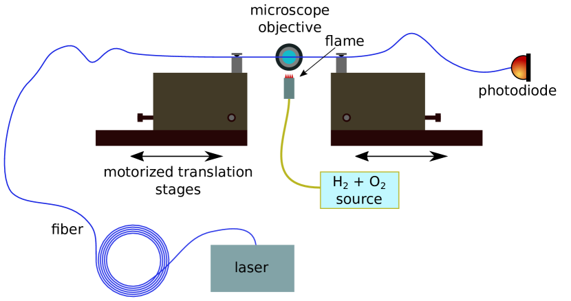
The fiber is suspended between two motorized platforms that can move horizontally and are controlled by a computer. A Bunsen burner is carefully positioned under the fiber and another motor controls its vertical position, and provide a controlled flame of \chH2 and \chO2. A photodiode, placed at the output of the fiber allows to monitor the transmission during the whole pulling process. In addition, the image of the fiber is collected by a microscope objective and recorded by a camera behind it: this is useful to correctly position the flame and to precisely adjust the vertical position of the flame during the pulling. When the pulling starts, the flame is placed at a given distance from the fiber and the motors start moving and pulling the fiber in order to reach the given shape. The movements needed to perform this operation depend not only on the chosen profile, but also on the physical characteristics of the flame, such as its size and temperature. The distance between the flame and the fiber, as well as the flux of hydrogen and oxygen need to be carefully chosen in order to obtain the same effective flame diameter used to calculate the profile itself, in our case . The effect of the flame size in the pulling procedure is described in [17]. With this system, we were able to reach fiber radius as small as and to reach transmissions over , but by accurately optimizing the shape of the tapered part even higher transmissions can be achieved [12].
In order to deposit a nanoemitter over the fiber, we create a drop of solution of containing the nanoemitters at the end of a micro-pipette. The next step is then to touch the NF with the drop repetitively until a particle gets stuck to it. For more precision, the whole process is controlled with a microscope and the micro-pipette is moved via precise translation stages.
Experimental apparatus
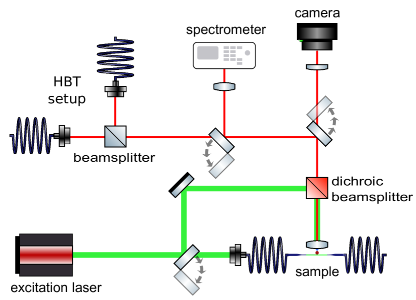
Our setup is represented in figure 2. By sending the light in the fiber we can excite the emitter and see the emission through the microscope: this is very convenient to detect the emitted light without having to care about the precise position of the emitter and to verify its single photon emission. If the coupling is good enough, we can also excite the nanoemitter through the microscope and collect the light from the fiber.
First results were obtained on our set-up with semiconductor nanocrystals that are well known to be good single photon emitters [18] and so well adapted for first tests. The emitters we used are dot-in-rod \chCdS/CdSe nanocrystals: this kind of nanocrystals have a core/shell structure which ensures a reduced blinking of the emission; moreover dots in rod have the specificity to have elongated shell that makes the emission to be polarized [19].
For that, we pulled a fiber with a diameter of in order to guide the light emitted by the nanocrystals. As a result, we were able to excite a single nanocrystal from the free space. The emitted light collected by the NF was enough to measure the photon autocorrelation function () using a Hanbury Brown and Twiss set-up (figure 3). For this experiment a pulsed excitation laser with a wavelength of was used. A clear signature of a single photon emitter was observed with a smaller than . This first result validates our experimental protocol for the use of other emitters and confirm that we can use different emitters in future experiments such as perovskite nanocrystals or silicon-vacancy centers in nanodiamonds as described further down.
2.2 Optical glass waveguides
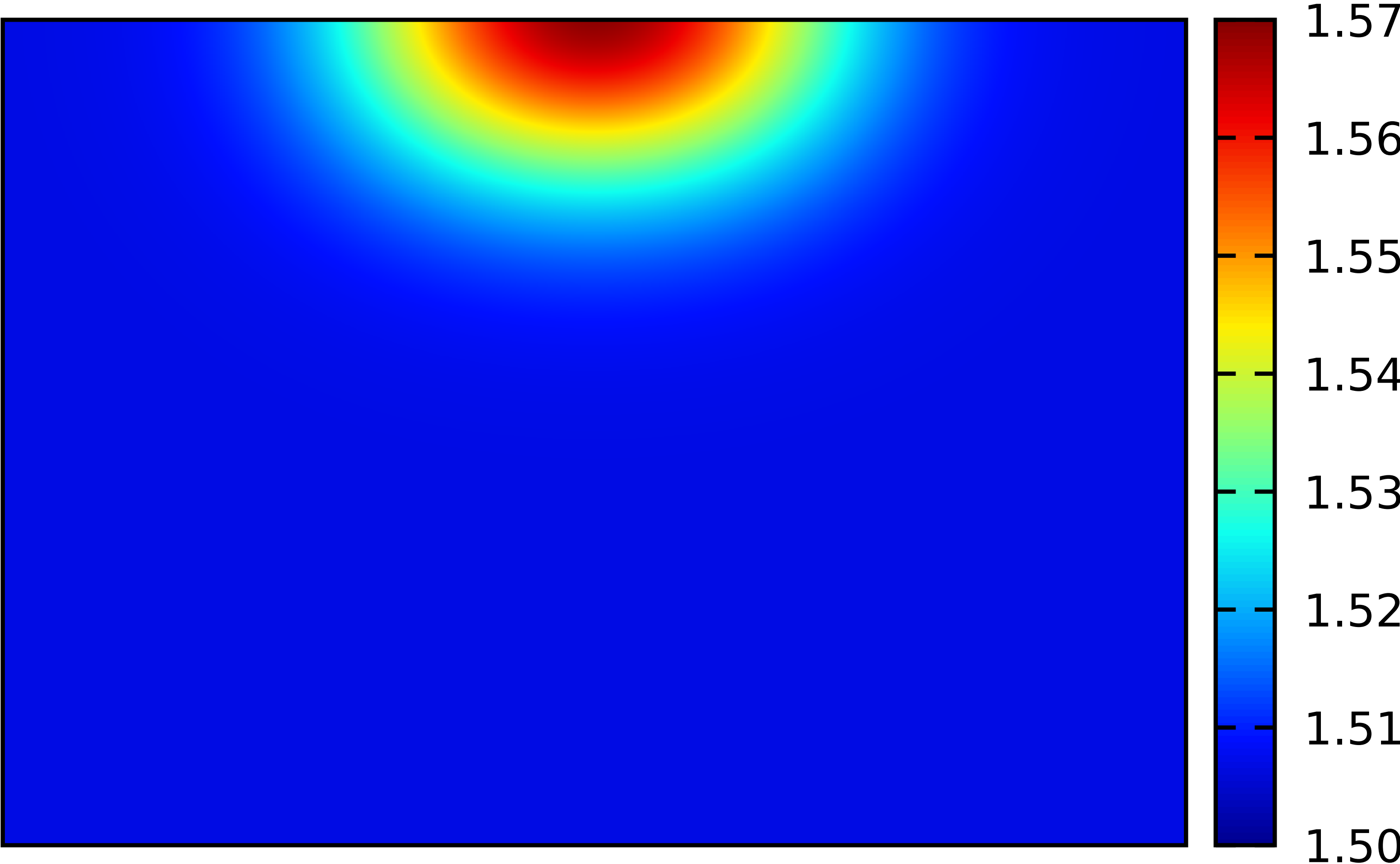
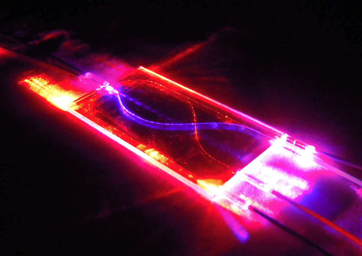
The notion of integrated optics was first introduced back in 1969 by S. E. Miller [20] with the revolutionary idea to reuse the planar technologies developed at the time for the microelectronics in order to fabricate optical circuits. Such devices opened up the way to compact, robust and self-aligned optical systems. Since the early years, the glass platform raised a great interest for many reasons. Indeed, glass waveguides show very low propagation losses – on the order of 0.1dB/cm – on a large bandwidth from visible to near-infrared wavelength, while ensuring a high coupling efficiency with optical fibers. In our case, these waveguides are realized on glass thanks to the ion-exchange technology known for centuries (with stained glasses) to change the glass color properties [21]. The waveguide core creation relies on the diffusion – either purely thermal or field assisted – of alkali ions into the glass substrate which induces in turn an increase of the refractive index. Different ionic species (\chTl+, \chK+, \chAg+) can be exchanged with the one hosted in the glass matrix (\chNa+ being the most common one) [22] resulting in a gradient-like profile. In order to make strip waveguides, the ion-exchange process is limited to a specific area using a photo-lithography technique. An example of a simulated index profile obtained for a 2m mask opening is depicted in figure LABEL:fig:Wave_tph_a. Such surface waveguide is designed to work in single mode operation at telecommunication wavelength. Figure LABEL:fig:Wave_tph_a shows the local increase of the index which is characterized by a low refractive index contrast, here. The first demonstration of an ion-exchanged waveguide (IEW) was achieved in 1972 [23] and the technology has been continuously investigated and developed since then [9]. As such, the glass optical platform is highly versatile and can offer both surface and buried waveguides designs as opposed to other techniques such as the laser-writing technique. For this technique, surface waveguiding is not possible and thus interaction with nanoemitters from the top is not possible. Borosilicate glasses are commonly used to implement passive features and to make complex circuitry. For instance a beam combiner implemented on a glass chip is illustrated in figure LABEL:fig:Wave_tph_b. The IEW are connected to optical fibers thanks to glass ferules as visible on the bottom right of figure LABEL:fig:Wave_tph_b ensuring a good coupling efficiency. Nowadays, optical glass waveguides are widely spread for many applications including telecommunication and sensing [9]. For instance, chemical analysis takes benefit of the evanescent field interaction of a surface waveguide [24] to perform absorption spectroscopy in harsh environment. The latter phenomenon can also be used to couple the light from a nanoemitter [25] for quantum applications. This is precisely the effect that we want to use for coupling nanoemitters (such as the ones described below) to these optical buses for photons.
3 Quantum Emitters
3.1 Perovskites nanocrystals
General description
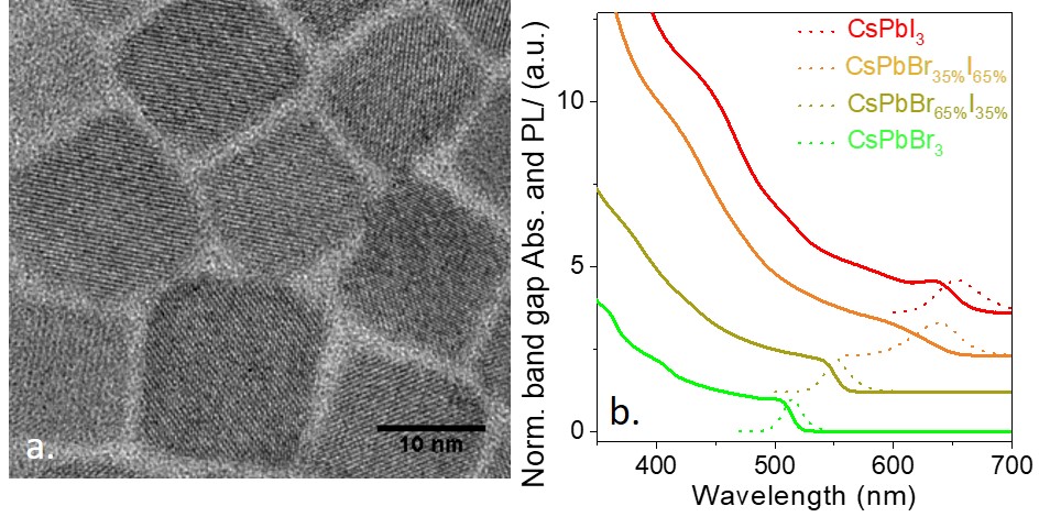
Nanocrystals are semiconductor nanoparticles with broadly tunable optical features from UV to THz [26]. Thanks to quantum confinement, atomic-like spectra can be obtained from such objects [27]. They thus appear to be an interesting candidate for quantum optics as single photon emission has been reported from them in the past [28]. Nevertheless, traditional II-VI semiconductor nanocrystals suffer from several issues. In particular, bright emission is only obtained through the growth of core shell heterostructures. Meanwhile, perovskite nanocrystals made of lead halide materials became very popular in the field of solar cells. Their defect-tolerant electronic structure leads to improved open-circuit voltage. It has been proposed to take advantage of this defect tolerance of lead halide perovskite to design bright core only nanocrystals [29]. The basic concept of the synthesis relies on the reaction of lead halide, in presence of long chain ligands made of oleic acid and oleylamine in a non coordinating solvent. At relatively low temperature (180 °C), the injection of a cesium oleate precursor leads to an immediate formation of \chCsPbX3 nanocrystals, with \chX=Cl, \chBr or \chI with cubic shape: this is clearly visible in figure 5a where a transmission electron microscopy image of \chCsPb(Br ;I)3 is shown. These particles have size around which is higher than the Bohr radius meaning their behaviour is very close to the bulk material. As for II-VI semiconductor nanocrystals, the band-edge energy can be tuned thanks to quantum confinement. Smaller nanocrystals can simply be obtained by reducing the growth temperature. However this is not the method the most commonly used. Conventional alloying is usually used. We can see in figure 5b the absorption and photoluminescence spectra of different alloying perovskite-nanocrystals in solution leading to different colors. The whole visible range can be spanned by tuning the X from \chCl to \chI. The most striking property of these perovskite nanocrystals comes from their high photoluminescence efficiency which ranges from to depending on the chosen halide. The investigation of the single particle property of \chCsPbX3 nanocrystals can easily be obtained by diluting them into a polystyrene matrix [30].
Optical characterization
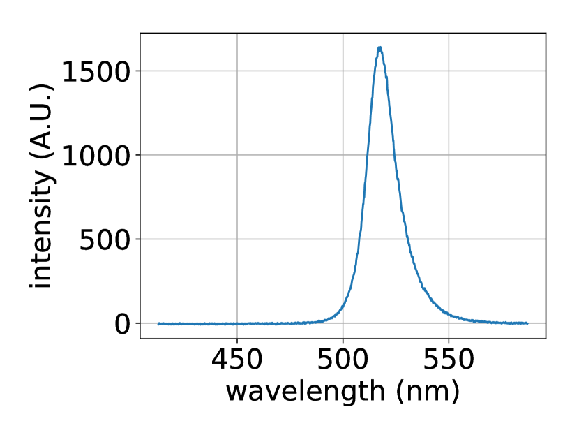
To study the emission spectra of these nanocrystals, we deposite them on a glass plate and use a confocal microscope to excite a single emitter with a pulsed excitation laser. The center wavalenghts of the spectra spread from to with a peak with a full width at half maximum (FWHM) of about . A typical spectrum is shown in figure 6.
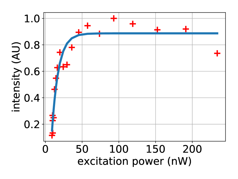
The emission of a single nanocrystal shows a clear saturation of the emitted light while increasing the excitation power, with a saturation power of (the curve is shown in Figure 7). Each experimental point is obtained by taking ten measurements and keeping only the three brightest ones. This procedure reduce the effect of blinking providing a most reliable result. The measurements of the Stokes parameters performed on our samples with the method illustrated in [31] have shown that the emission is not polarized.
Quantum properties
Antibunching measurements were performed using a Hanbury Brown and Twiss setup showing that some of the emitters had a clear single photon emission, with a . With our setup we can measure the for long values of (up to hundreds of ). This feature allows us to normalize the function at large delays, taking into account the bunching effect due to the blinking. This effect has to be considered in order to identify the real quality of the emitter and it is taken in consideration for the first time for perovskite nanocrystals.
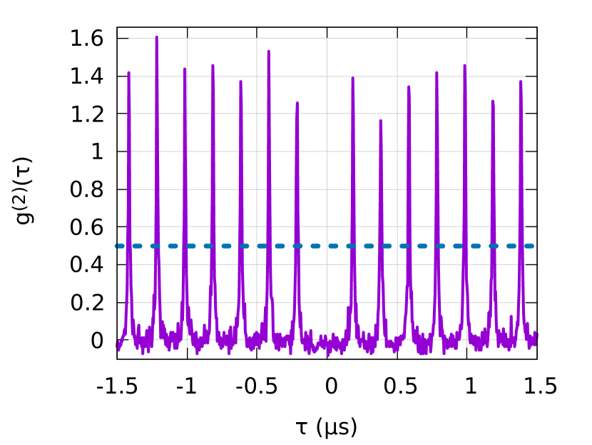
The result of the photon antibunching is shown in figure 8. The experimental curves are normalized using the peaks at a long delay , after having subtracted the background noise, estimated using the values between two different peaks. To perform the measurement, we use a PicoHarp 800 with a router that registers the full history of the detected photons. There is a limitation as two events occurring with a delay smaller than cannot be registered and thus creating an artificial flat region that has been removed from the signal for more clarity. A blue line indicates the threshold under which the emitter can be regarded as a single photon one. We can also note that the blinking of the emitter creates a bunching effect, that is clearly visible as the other peaks are higher than : this kind of effect was previously observed also with other types of emitters [32, 33].
3.2 \chSiV defect centers in nanodiamonds
3.2.1 Silicon-vacancy defect centers
Color center defects in diamond have become one of the leading research subjects in recent years due to their attractive optical properties. Among these, silicon vacancy (\chSiV) centers are very promising thanks to their attractive features, such as high brightness [34], narrow inhomogeneous distribution [35], stable single photon emission (even at room temperature) and minimal spectral diffusion [36]. These properties of \chSiV are desirable for quantum photonics especially for quantum information [37], quantum communication [38] and quantum networks [10]. Bulk diamond induces a low extraction of single photons from \chSiV centers due to its high refractive index (). To overcome this problem, diamond nanostructures have been adopted. They can be spatially manipulated and positioned to enhance coupling to other nanophotonics structures or to fibers. Here, we explore the possibility of controlling the nanodiamonds size distribution and photoluminescence of \chSiV centres by varying growth conditions. We perform room-temperature characterization of several ND samples grown using the high pressure/high temperature (HPHT) method [39]. Previously, it has been found that nanodiamonds grown with this method host \chSiV centers with excellent optical properties [40]. They are, however, limited by effects due to the surface of the nanodiamonds. In this article, we explore this issue by studying the influence of the growth temperature and the treatment of the surface with mixture of acids on the physical and optical properties of our nanodiamonds. Table 1 shows the growth conditions for different nanodiamonds samples A, B and C.
3.2.2 Growth of nanodiamonds containing SiV centers
The NDs with \chSiV centers used in this work were synthesized using the same high-pressure high-temperature (\ch8GPa) method described in ref [39], based on mixtures of naphthalene (\chC10H8), \chCF1,1 (fluorographite) and tetrakis(trimethylsilyl) silane (\chC12H36Si5, Strem Chemicals Co.) was used as the main silicon doping addition. The samples studied here are different in terms of growth temperature and surface treatment. Two temperatures were studied here, (B) and (A and C), to explore the effect on the size of the NDs. In addition, acid treatment is studied here to explore its effect on the shape and the crystallinity of the nanodiamonds (samples A and C).
| Sample | Si/C ratio | Temperature (∘C) | Treatment |
|---|---|---|---|
| A | Acid | ||
| B | Acid | ||
| C | —– |
3.2.3 Experimental setup
To analyze the optical properties of the SiV centers in nanodiamonds, we use a home-built microphotoluminescence set-up at room temperature, as described in the following.A He-Ne laser with a wavelength of excites the sample through an air microscope objective (, ). The emission passes through a high pass filter (above 700 nm) so that the excitation light is rejected. It is then directed to either a grating spectrometer ( resolution) for photoluminescence measurements or to a multimode fiber ( core) that acts as a pinhole. In the second case, the emission is sent afterwards to a Hanbury Brown and Twiss setup. The latter consists of a 50/50 beam-splitter and two avalanche photodiodes (APD) that are used for single photon counting to measure the second-order correlation function. Finally, a narrow-band filter (13 nm bandwidth around 740 nm) is placed in front of each APD. The purpose of these filters is double: i- they remove all background emission and ii- they eliminate the cross talk between the APDs.
3.2.4 Emission properties of the SiV centers
Optical properties: photoluminescence
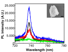
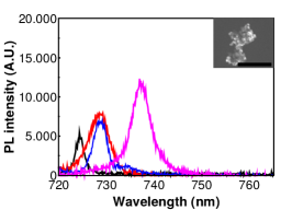
Photoluminescence measurements of stable \chSiV centers in sample A () revealed fluorescence peaks at the typical wavelength with a zero phonon line (ZPL) at and with a visible phonon sideband (see Figure LABEL:fig:sampleA). As for SiV defects in sample B ( ), they suffer from surface effect from a highly strained nanodiamonds, revealed in an inhomogeneous distribution of the ZPL varying between and .(see Figure LABEL:fig:sampleB). Similar observation of local strain in smaller nanodiamonds were reported elsewhere [41] [34]. The tiny size of nanodiamonds is coming from the fact of lower growth temperature.
Physical properties: morphology
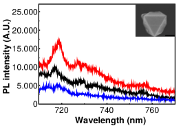
Figure LABEL:fig:sampleC presents a highly crystalline nanodiamond under our electron microscope and yet, despite the crystalline quality of the nanodiamonds in sample C , no emission of \chSiV centers was found. The PL spectra show a clear signature of graphite though (peak at ). We deduce that the non-treatment of sample C with acid favours other defects and impurities at the surface, such as surface contamination and graphitization which induces the quenching of luminescence. Sample A was grown at the same temperature but was subjected to acid treatment and clearly presents nice photoluminescence at or so Figure LABEL:fig:sampleA. Such acid treatment is thus needed to prevent the contamination and graphitization on the surface of nanodiamonds.
4 Towards coupling of nanoemitters using nanophotonics
The recent results developed in this article put the bricks down towards a new integrated photonics platform based on nanophotonics. Figure 10
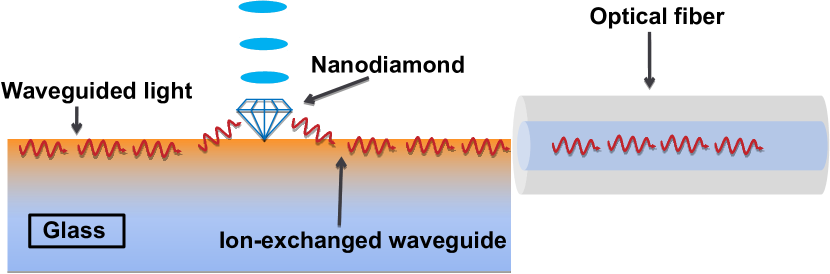
presents a schematic of what a final structure would look like. We see a nanodiamond excited from the top and with its fluorescence coupled into the ion-exchange waveguide (side view). The photons can then be coupled to an optical fiber either using butt-coupling or by proper connectic between the fiber and the waveguide. Several issues remain to be dealt with in order to optimize this system such as an efficient interface between the nanoemitter and the waveguide. Different approaches are being explored such as the use of a plasmonic nanoantenna [42] or the deposition of a thin layer a proper-matched refractive index layer [25] or a combination of both. One this is taken care of, we still need to deal with the positioning of the nanoemitter at the right place on the waveguide which as a certain width between 1 to 2 µm. This crucial step is also investigated with different approaches such as the placing of the emitters using surface functionalisation or using an AFM tip [43]. In the near future, it would probably be even more benefic to use a very thin diamond membrane to put directly on the waveguide for better coupling.
5 Conclusion & perspectives
In this article, we presented two nanophotonics platform for efficient coupling of light with nanoemitters. We also presented recent novel results on the optical properties of perovskite nanocrystals, including quantum optical properties, as well as some results on the effect of growth and treatment on nanodiamonds monitored by the fluorescence of SiV centers. We finally explored a way towards a fully intergrated platform where light from nanoemitters is emitted directly into an optical fiber. This opens up new possibilities such as the use of the ion-exchange waveguide and nanofibers as optical buses between 2 or more nanoemitters. The potential scalability of our nanophotonic platforms is clear to us but many developements remain to be done.
Acknowledgements
The authors would like to thank Régis Deturche, Aurélie Broussier and Xiaolun Xu from the UTT and Robert Taylor from the University of Oxford for their assitance. The authors would like to acknowledge the funding from the COST Action Nanoscale Quantum Optics, from the ITN project LIMQUET as well as the ANR projects SINPHONIE and Iper-nano2. AB et QG are members of the "Institut Universitaire de France" (IUF).
References
- [1] A. Acín, I. Bloch, H. Buhrman, T. Calarco, C. Eichler, J. Eisert, D. Esteve, N. Gisin, S. J. Glaser, F. Jelezko, et al., New J. Phys. 2018, 20, 8 080201.
- [2] A. Vamivakas, A. Sergienko, A. Fiore, J. Opt. 2017, 19, 8 080403.
- [3] D. P. DiVincenzo, Fortschritte der Physik: Progress of Physics 2000, 48, 9-11 771.
- [4] P. Krantz, M. Kjaergaard, F. Yan, T. P. Orlando, S. Gustavsson, W. D. Oliver, Applied Physics Reviews 2019, 6, 2 021318.
- [5] B. E. Kane, Nature 1998, 393, 6681 133.
- [6] D. Loss, D. P. DiVincenzo, Phys. Rev. A 1998, 57, 1 120.
- [7] L. Childress, R. Hanson, MRS Bull. 2013, 38, 2 134.
- [8] R. Black, E. Gonthier, S. Lacroix, J. Lapierre, J. Bures, In Components for Fiber Optic Applications II, volume 839. International Society for Optics and Photonics, 1988 2–19.
- [9] A. Tervonen, S. K. Honkanen, B. R. West, Opt. Eng. 2011, 50, 7 071107.
- [10] A. Sipahigil, R. E. Evans, D. D. Sukachev, M. J. Burek, J. Borregaard, M. K. Bhaskar, C. T. Nguyen, J. L. Pacheco, H. A. Atikian, C. Meuwly, et al., Science 2016, 354, 6314 847.
- [11] A. Stiebeiner, R. Garcia-Fernandez, A. Rauschenbeutel, Opt. Express 2010, 18, 22 22677.
- [12] R. Nagai, T. Aoki, Opt. Express 2014, 22, 23 28427.
- [13] T. A. Birks, Y. W. Li, Journal of Lightwave Technology 1992, 10, 4 432.
- [14] F. Le Kien, J. Liang, K. Hakuta, V. Balykin, Opt. Commun. 2004, 242, 4-6 445.
- [15] K. P. Nayak, K. Hakuta, New J. Phys. 2008, 10, 5 053003.
- [16] M. Joos, C. Ding, V. Loo, G. Blanquer, E. Giacobino, A. Bramati, V. Krachmalnicoff, Q. Glorieux, Phys. Rev. Appl 2018, 9, 6 064035.
- [17] J. Hoffman, Ph.D. thesis, University of Maryland, College Park, 2014.
- [18] P. Michler, A. Imamoğlu, M. Mason, P. Carson, G. Strouse, S. Buratto, Nature 2000, 406, 6799 968.
- [19] F. Pisanello, L. Martiradonna, G. Leménager, P. Spinicelli, A. Fiore, L. Manna, J.-P. Hermier, R. Cingolani, E. Giacobino, M. De Vittorio, et al., Appl. Phys. Lett. 2010, 96, 3 033101.
- [20] S. E. Miller, The Bell System Technical Journal 1969, 48, 7 2059.
- [21] P. Mazzoldi, S. Carturan, A. Quaranta, C. Sada, V. Sglavo, Riv Nuovo Cimento 2013, 36 397.
- [22] J.-E. Broquin, In Integrated Optics Devices V, volume 4277. International Society for Optics and Photonics, 2001 105–117.
- [23] T. Izawa, H. Nakagome, Appl. Phys. Lett. 1972, 21, 12 584.
- [24] T. Allenet, F. Geoffray, D. Bucci, F. Canto, P. Moisy, J.-E. Broquin, Opt. Eng. 2019, 58, 6 060502.
- [25] J. B. Madrigal, R. Tellez-Limon, F. Gardillou, D. Barbier, W. Geng, C. Couteau, R. Salas-Montiel, S. Blaize, Appl. Opt. 2016, 55, 36 10263.
- [26] N. Goubet, A. Jagtap, C. Livache, B. Martinez, H. Portalès, X. Z. Xu, R. P. Lobo, B. Dubertret, E. Lhuillier, J. Am. Chem. Soc. 2018, 140, 15 5033.
- [27] C. B. Murray, D. J. Norris, M. G. Bawendi, J. Am. Chem. Soc. 1993, 115, 19 8706.
- [28] X. Brokmann, E. Giacobino, M. Dahan, J.-P. Hermier, Appl. Phys. Lett. 2004, 85, 5 712.
- [29] L. Protesescu, S. Yakunin, M. I. Bodnarchuk, F. Krieg, R. Caputo, C. H. Hendon, R. X. Yang, A. Walsh, M. V. Kovalenko, Nano Lett. 2015, 15, 6 3692.
- [30] G. Raino, A. Landuyt, F. Krieg, C. Bernasconi, S. T. Ochsenbein, D. N. Dirin, M. I. Bodnarchuk, M. V. Kovalenko, Nano Lett. 2019.
- [31] H. G. Berry, G. Gabrielse, A. Livingston, Appl. Opt. 1977, 16, 12 3200.
- [32] M. Manceau, S. Vezzoli, Q. Glorieux, E. Giacobino, L. Carbone, M. De Vittorio, J.-P. Hermier, A. Bramati, ChemPhysChem 2018, 19, 23 3288.
- [33] S. Ulrich, M. Benyoucef, P. Michler, N. Baer, P. Gartner, F. Jahnke, M. Schwab, H. Kurtze, M. Bayer, S. Fafard, et al., Phys. Rev. B 2005, 71, 23 235328.
- [34] E. Neu, D. Steinmetz, J. Riedrich-Möller, S. Gsell, M. Fischer, M. Schreck, C. Becher, New J. Phys. 2011, 13, 2 025012.
- [35] H. Sternschulte, K. Thonke, R. Sauer, P. Münzinger, P. Michler, Phys. Rev. B 1994, 50, 19 14554.
- [36] L. J. Rogers, K. D. Jahnke, T. Teraji, L. Marseglia, C. Müller, B. Naydenov, H. Schauffert, C. Kranz, J. Isoya, L. P. McGuinness, et al., Nat. Commun. 2014, 5 4739.
- [37] S. Prawer, I. Aharonovich, Quantum information processing with diamond: Principles and applications, Elsevier, 2014.
- [38] C.-H. Su, A. D. Greentree, L. C. Hollenberg, Phys. Rev. A 2009, 80, 5 052308.
- [39] V. A. Davydov, A. Rakhmanina, S. Lyapin, I. Ilichev, K. N. Boldyrev, A. Shiryaev, V. Agafonov, JETP Lett. 2014, 99, 10 585.
- [40] L. J. Rogers, O. Wang, Y. Liu, L. Antoniuk, C. Osterkamp, V. A. Davydov, V. N. Agafonov, A. B. Filipovski, F. Jelezko, A. Kubanek, Phys. Rev. Appl 2019, 11, 2 024073.
- [41] E. Neu, C. Hepp, M. Hauschild, S. Gsell, M. Fischer, H. Sternschulte, D. Steinmüller-Nethl, M. Schreck, C. Becher, New J. Phys. 2013, 15, 4 043005.
- [42] A. Apuzzo, M. Février, R. Salas-Montiel, A. Bruyant, A. Chelnokov, G. Lérondel, B. Dagens, S. Blaize, Nano Lett. 2013, 13, 3 1000.
- [43] A. Cuche, A. Drezet, Y. Sonnefraud, O. Faklaris, F. Treussart, J.-F. Roch, S. Huant, Opt. Express 2009, 17, 22 19969.