Electronic and Magnetic Characterization of Epitaxial VSe2 Monolayers on Superconducting NbSe2
Abstract
Vertical integration of two-dimensional (2D) van der Waals (vdW) materials with different quantum ground states is predicted to lead to novel electronic properties that are not found in the constituent layers. Here, we present the direct synthesis of superconductor-magnet hybrid heterostructures by combining superconducting niobium diselenide (NbSe2) with the monolayer (ML) vanadium diselenide (VSe2). More significantly, the in-situ growth in ultra-high vacuum (UHV) allows to produce a clean and an atomically sharp interfaces. Combining different characterization techniques and density-functional theory (DFT) calculations, we investigate the electronic and magnetic properties of VSe2 on NbSe2. Low temperature scanning tunneling microscopy (STM) measurements demonstrate a reduction of the superconducting gap on VSe2 layer. This together with the lack of charge density wave signatures indicates magnetization of the sheet, at least on the local scale. However, overall, VSe2 does not behave as a conventional ferromagnet.
keywords:
transition metal dichalcogenides, vertical heterostructure, superconductor, magnetism, vanadium diselenide VSe2, niobium diselenide NbSe2, scanning tunneling microscopyCentro de Física de Materiales (CSIC-UPV-EHU), Manuel Lardizábal 4, 20018 San Sebastián, Spain \alsoaffiliationCentro de Física de Materiales (CSIC-UPV-EHU), Manuel Lardizábal 4, 20018 San Sebastián, Spain \alsoaffiliationIkerbasque, Basque Foundation for Science, 48013 Bilbao, Spain
There has been a surge of interest in designer materials that would realize electronic responses not found in naturally occurring materials. There are many routes towards this goal and they are all being explored vigorously: e.g., artificial atomic lattices1, 2, 3, 4, 5, atomically precise graphene nanoribbons6, 7, 8, and controlled heterostructures of two-dimensional materials 9, 10, 11, 12, 13, 14, 15. The designer concept is well illustrated in systems combining magnetism with superconductivity to realize topological superconductivity 16, 17, 18, 19, 20. Individual magnetic impurity atoms give rise to so-called Yu-Shiba-Rusinov states 21, which can be coupled in extended structures to give rise to bands (inside the superconducting gap). Eventually, the system can be driven into a topological phase in the presence of certain spin textures or spin-orbit coupling 18, 22, 23, 24, 25, 26. Topological superconductors are a distinct form of matter that is predicted to host boundary Majorana fermions. Experimental realization of Majorana fermions is exciting in its own right, but this is compounded by the proposal that systems with non-abelian statistics can serve as the basis for topological quantum computation27, 28, 29. Experimentally, these systems have been realized in one-dimensional chains of magnetic adatoms on the surface of s-wave superconductors18, 23, 30 and this has been extended to two-dimensional systems by using magnetic metal islands 31, 32. However, these types of systems can be sensitive to disorder and interface engineering through, e.g., the use of an atomically thin separation layer, might be required 32.
Issues with interface inhomogeneities can potentially be avoided in van der Waals (vdW) heterostructures, where the different layers interact only through vdW forces 9, 10. Layered materials that remain magnetic down to the monolayer (ML) limit have been recently demonstrated 11, 12. While the first reports relied on mechanical exfoliation for the sample preparation, related materials CrBr3 and Fe3GeTe2 have also been grown using molecular-beam epitaxy (MBE) in ultra-high vacuum (UHV) 33, 34. This is essential for realizing clean edges and interfaces. Very recently, monolayer magnetism was suggested in the transition metal dichalcogenide (TMD) vanadium diselenide (VSe2), which can be readily grown using MBE on various layered materials 13. Later reports have questioned the existence of magnetism in VSe2 as no magnetic signal was detected in X-ray magnetic circular dichroism (XMCD) experiments 35, 36. Angle-resolved photoemission spectroscopy revealed an enhanced charge-density wave (CDW) transition at a higher temperature than in the bulk, and it was suggested that the presence of CDW driven by Fermi-surface nesting removes the usual mechanism for achieving a magnetic ground state 37, 38, 35, 39. It has also been suggested that spin frustration plays a role in VSe2 samples grown by MBE 36. Support for this comes from recent experiments on chemically exfoliated VSe2 flakes that show ferromagnetic behaviour with a Curie temperature of ca. 470 K and also non-zero XMCD signal 40. While there still is no consensus on the nature of the possible magnetic ground state of VSe2, it is clear that there is a delicate balance between different competing interacting states and phases in monolayer transition-metal dichalcogenides, which may also depend on the nature of the substrate.35, 39, 36, 41, 42, 43, 40
Combining 2D magnetic and superconducting TMDs would create a promising material platform for investigating the coexistence of superconductivity, magnetism and the resulting emergent quantum phases of matter. The inherent lack of surface bonding sites due to the layered nature of these materials prevents chemical bonding between the layers and results in a better control of the interfaces. We report growth of single layer vanadium diselenide (VSe2) by molecular beam epitaxy on superconducting niobium diselenide (NbSe2) substrate and study the magnetic and electrical properties of these heterostructures. MBE growth under UHV conditions facilitates the formation of clean edges and interfaces and we characterize the electronic structure of the resulting hybrid materials down to the atomic scale using low-temperature scanning tunneling microscopy (STM) and spectroscopy (STS). Our results give further experimental information on the magnetic properties of VSe2 and demonstrate a clean and controllable platform for creating superconducting-magnetic hybrid TMD materials with great potential of integrating TMDs into future electronics devices.
1 Results and discussion
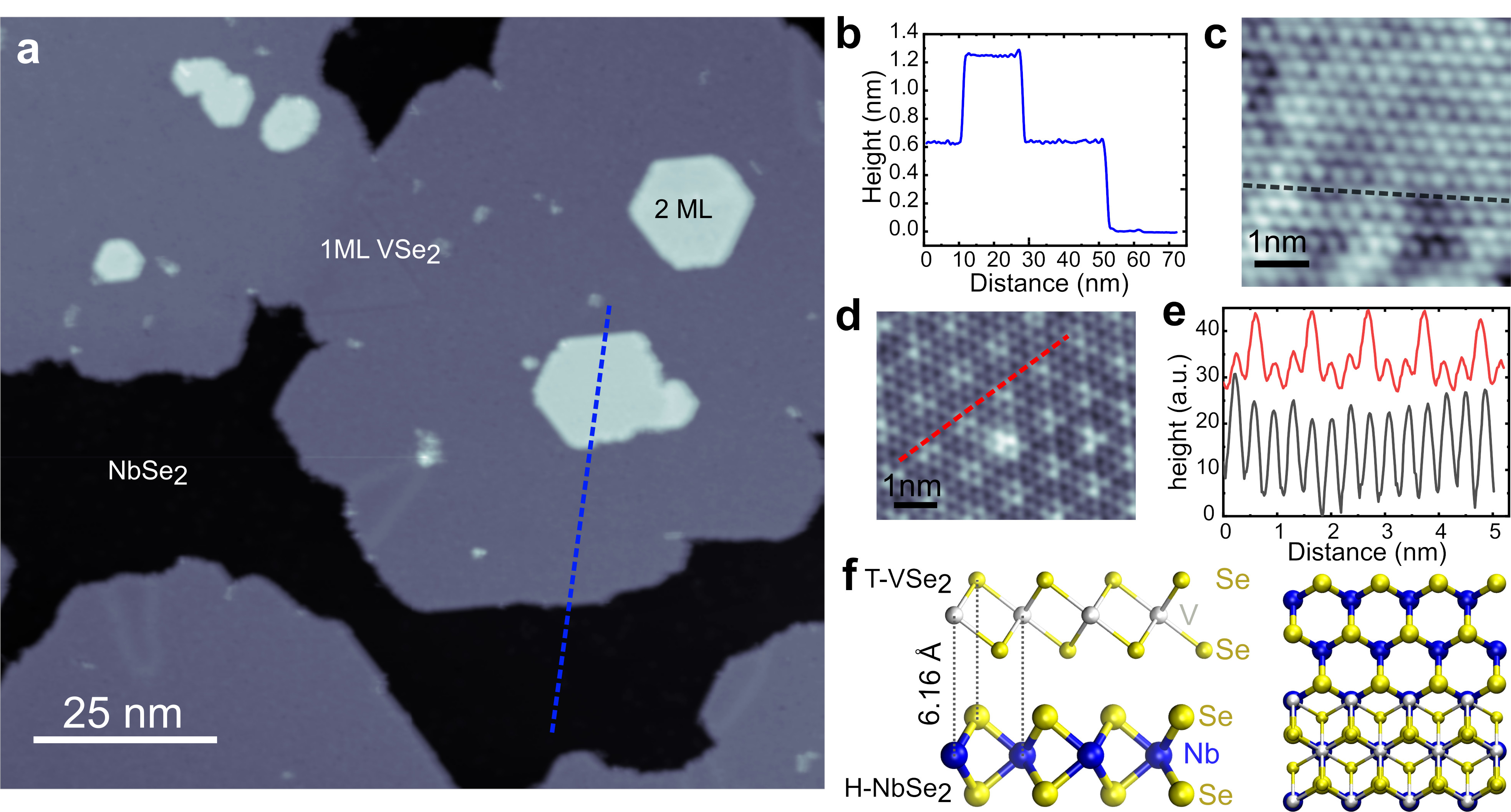
VSe2 was grown on NbSe2 by MBE and results are illustrated in Fig. 1 (see Methods for details). Briefly, vanadium was evaporated under excess flux of selenium onto a NbSe2 crystal cleaved in-situ in UHV and held at K during the growth. The samples were characterized in-situ by STM and X-ray photoelectron spectroscopy (XPS). In addition, after capping the films with a thick Se layer, the samples were characterized ex-situ by temperature dependent magnetization measurements. Fig. 1a shows STM characterization of sub-monolayer VSe2 films on NbSe2 substrate. VSe2 grows atomically smooth, large uniform ML islands. Higher coverages result in the formation of a second layer. The profile along the blue line in Fig. 1a shows that the apparent height of the VSe2 film is 6.5 Å(Fig. 1b) consistent with the unit cell height 44. Atomically resolved STM images of the VSe2 monolayer and NbSe2 crystal surface are shown in Figs. 1c and 1d, respectively. While NbSe2 shows the well-known charge-density wave modulation in the atomic contrast, we do not detect a charge density wave on VSe2 (even at temperature of K). This is in contrast to reports on HOPG and bilayer graphene substrates13, 35, 37. The lattice constants can be measured from the atomically resolved images, as depicted in Fig. 1e. This yields values of Å and Å for VSe2 and NbSe2, respectively. These values match well with previous experimental results44, 38, 45. The lattice mismatch is roughly 3%; this together with the fact that we observe several different orientations of VSe2 w.r.t. the underlying NbSe2 suggests that there is no lattice match between VSe2 and NbSe2.
XPS was used to study the chemical composition of the as-grown VSe2 films on NbSe2. Characteristic peaks of V, Se and Nb are found in the XPS spectra (see Supporting Information (SI) Fig. S1). The binding energies of the V 2p3/2 peak at 513.7 eV and the Se 3d5/2 peak at 53.4 eV are similar to those previously observed for VSe2 on HOPG45, 13. The Nb 3d5/2 peak is found at 203.5 eV which is typical for NbSe2. Both VSe2 and NbSe2 have similar selenium binding energies and thus they cannot be resolved from the Se 3d spectrum 46. The V:Se:Nb stoichiometry for a 0.6 ML VSe2 film was found to be roughly 1:5:2 (estimated from integrated peak areas which were normalized to the elements’ atomic sensitivity factors). No other elements, such as possible magnetic impurities, were detected above the detection limit of 1 atomic percent.
We have complemented the experiments by density functional theory (DFT) calculations (see Methods and SI for details). Fig. 1f shows the fully relaxed geometry of VSe2/NbSe2 heterostructure from the side and top views. The energetically most favourable stacking has the lower layer Se atoms of VSe2 on top of hollow site of the NbSe2 (2.94 Å from Se in NbSe2 to Se in VSe2) and V on top of Nb, with a distance of 6.16 Å from Nb to V.
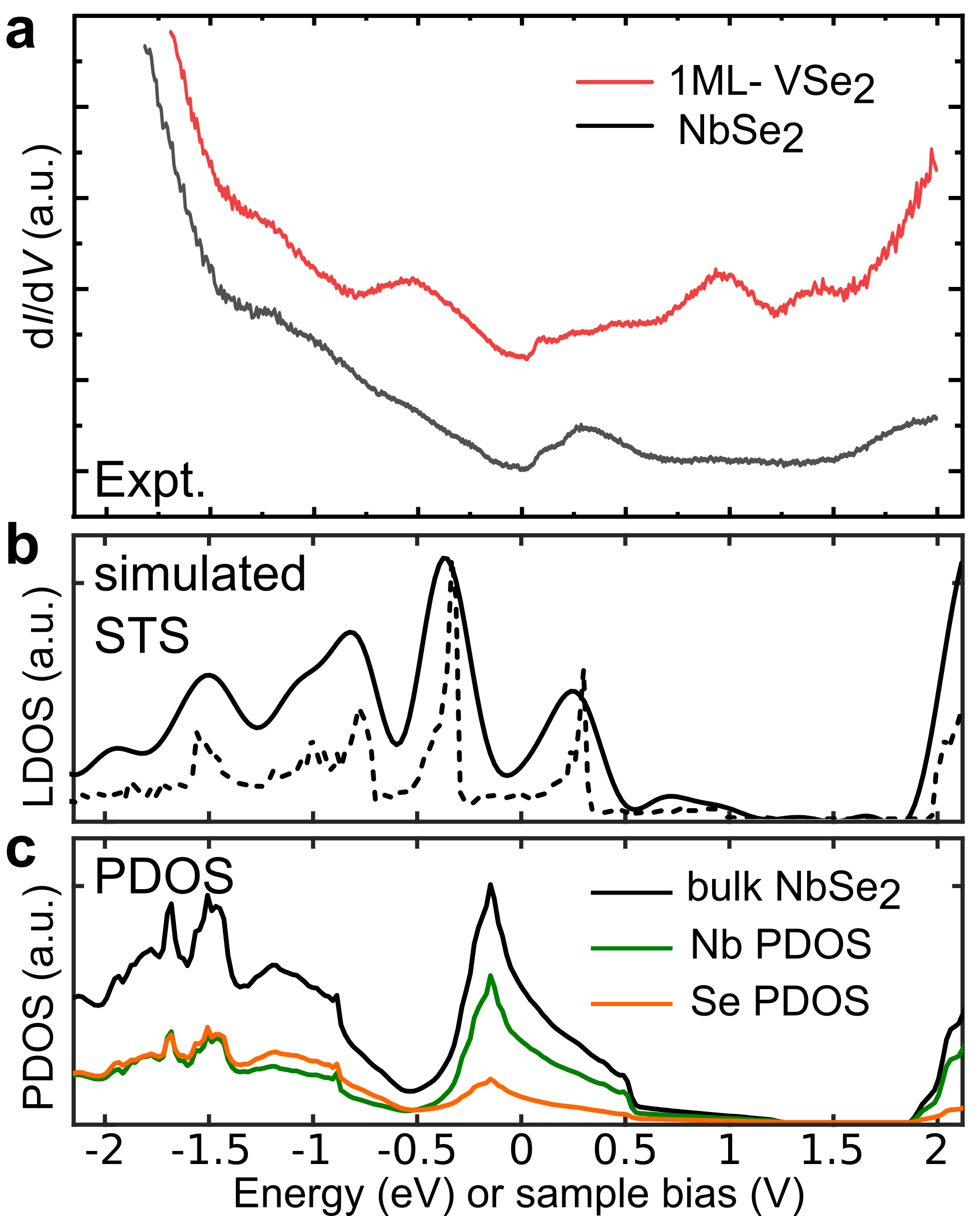
We have probed the electronic structure of single-layer VSe2/NbSe2 heterostructure by both scanning tunnelling spectroscopy (STS) and DFT. Fig. 2a shows typical d/d spectra taken on the ML VSe2 and on the bulk NbSe2 substrate over a large bias range. We will first focus on the NbSe2 response. At positive bias (empty states) region, the most pronounced features on bulk NbSe2 are the broad resonances at V and V, while at negative bias the d/d signal is broad and rising. The measured d/d spectrum on NbSe2 is in agreement with earlier STS studies on bulk NbSe247. The features in our d/d spectroscopy also match the simulated spectra on a 3-layer slab of NbSe2 (Fig. 2b) and can be compared with the bulk density of states (Fig. 2c). The first resonance at positive bias arises from the Nb-derived band, while the broad feature at negative bias overlaps with the mostly selenium derived bands below . On VSe2, at positive bias, there are pronounced features close to the Fermi level and also at 0.9 V and 1.45 V. At negative bias, we observe a peak at -0.5 V, and a shallow feature at V. These VSe2 features are discussed in more detail below.
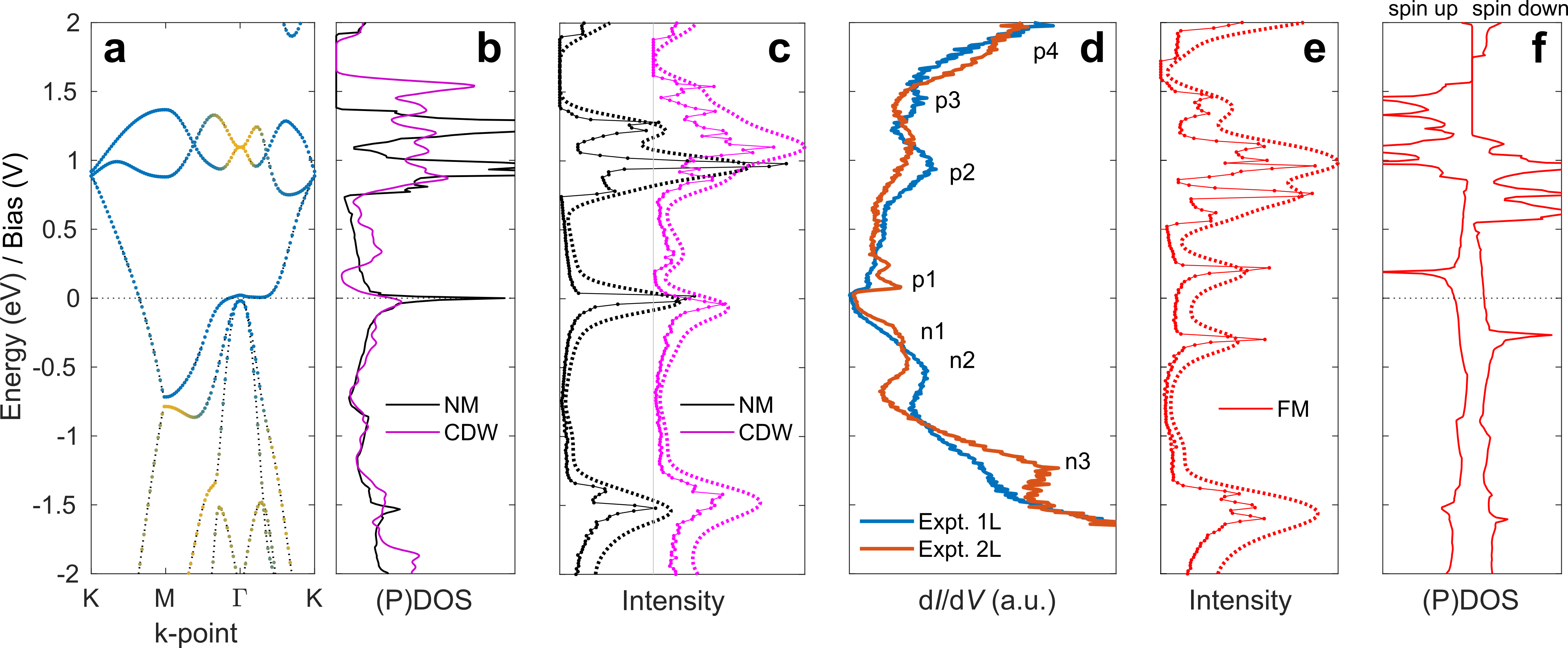
The electronic structure and the simulated and experimental STS are shown in Fig. 3. First focusing on the experimental spectra for monolayer and bilayer VSe2 in Fig. 3d, we observe peaks close to the Fermi level at both positive and negative bias and they are more pronounced for the bilayer compared to the monolayer. Their energy spacing (gap) is eV with an abrupt edge at positive energy (peak p1) and smoother edge at negative energy that develops to peaks labelled with n1/n2. At larger positive or negative bias, several peaks can be distinguished with the peak positions shifting between the mono- and bilayer spectra.
Starting from the non-magnetic (NM) phase, the band structure shows the partially filled d-band (Fig. 3a). There is a flat region between and K-points, which also happens to coincide with the Fermi-level. This leads to a strong peak at the Fermi-level in the DOS and also in the simulated STS, which obviously contrasts the experimental spectra. NM phase is also unstable in calculations and may either develop CDW or ferromagnetism, depending on conditions (strain, doping, defects) and on computational parameters (see SI). In the CDW phase, DOS exhibits a clear pseudogap formation, although not at the Fermi-level, but just above it. While the simulated STS would be relatively consistent with the experimental one, we do not detect CDW in the STM topography and also do not observe a hard gap at the Fermi-level as reported in Ref. 13.
In the ferromagnetic (FM) phase, the spin-up and -down band structures are only shifted in energy as in itinerant FM. The calculated magnetic moment depends moderately on strain and the computational parameters (e.g. the Hubbard ), see SI for details 48. Consequently also the DOS and simulated STS show splitting of the peaks w.r.t. NM phase. Due to the splitting of the DOS peak at Fermi-level, the lower branch could explain the peaks n1/n2 with the higher branch falling slightly above Fermi-level (feature p1 in the experimental spectra). The FM phase also seems to yield better agreement between the simulated and experimental STS for the peaks p2 and p3 in the monolayer sample. Even though the magnetic response of VSe2 is rather complex, at the atomic scale features in the STS spectra seem to have better match with the FM phase than the CDW phase.
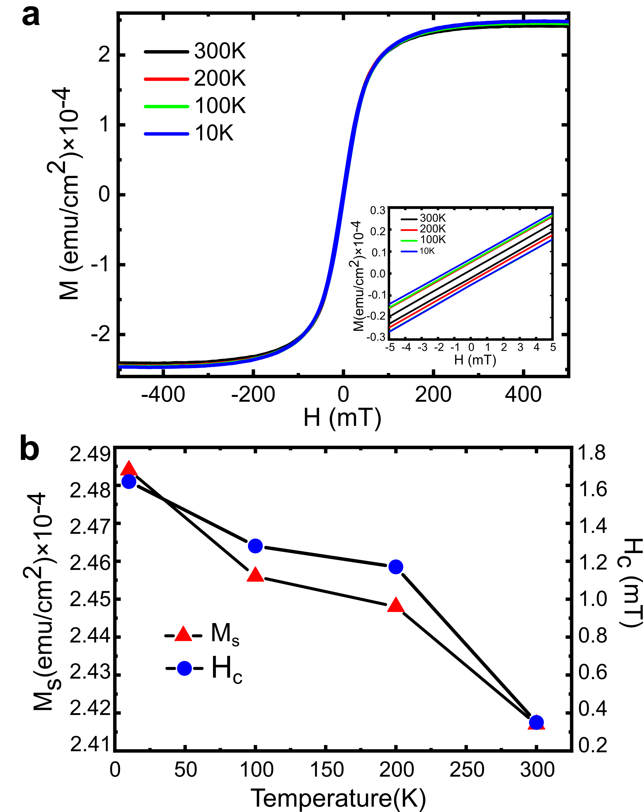
After the electronic characterization of the samples, we will next focus on their magnetic properties. To explore the magnetic properties of ML VSe2 on NbSe2, we carried out magnetization measurements at various sample temperatures (See Methods for details). All the VSe2 samples measured showed an in-plane magnetic response similar to that shown in Fig. 4a, where the loops have a vanishing coercivity and remanence, but show saturation around mT 38. A paramagnetic background has been subtracted from this data (see SI Fig. S14; Fig. S15 shows a direct comparison between the substrate and VSe2 responses). As shown in Fig. 4b, the coercive field is very small and it and saturation magnetization are practically independent of temperature in the range of K. While the mechanism is different here, there are other systems that exhibit phenomenologically similar magnetic responses 49, 50. This behaviour is inconsistent with standard ferromagnetism and it has been suggested that spin frustration plays a role in samples grown by MBE 36, 40. Experiments on chemically exfoliated VSe2 flakes exhibit ferromagnetic response with a Curie temperature of ca. 470 K 40. The point on these experiments was that chemical exfoliation from the bulk results in macroscopic single-crystalline flakes of VSe2 that then exhibit the expected magnetic response. As there is no strict alignment between the substrate and the VSe2 layer, MBE growth results in a polycrystalline 2D layer, which also may be affected by substrate interactions. However, local measurements (such as STM) should still probe the ferromagnetic phase that corresponds to the DFT calculations.
It has been argued that there is no conventional ferromagnetism in VSe2 on graphite and graphene substrates37, 38, 35, 36, 43. Here, one potentially important difference between our samples and those on graphite and graphene is the absence of a charge-density wave: we find no evidence of CDW in either the STM images or the d/d spectroscopy (see below). The stability of the CDW according to our DFT calculations is extensively discussed in the SI. Furthermore, in previous studies 13, monolayer VSe2 sample exhibits a maximum in and in a range around K and this non-monotonic behaviour is ascribed to the CDW transition. This is in contrast to our data on and as a function of temperature. The absence of CDW transation is also independently determined from the magnetization measurement under zero-field-cooled (ZFC) and field-cooled (FC) regimes, where we do not observe noticeable changes in the slope of the ZFC and FC curves due to the CDW (see SI Fig. S16).
The magnetic response of the sample below the superconducting transition temperature ( K) is dominated by the superconducting NbSe2 substrate. Magnetization curves measured at 2 K for bulk NbSe2 and VSe2/NbSe2 (see SI Fig. S16) show superconducting diamagnetic behavior as reported previously51, 52. Moreover, there is no obvious difference between these magnetization curves, which indicates that the signal is mostly dominated by the bulk NbSe2. This conclusion is further supported by the temperature dependent magnetization curves for the zero-field cooling (ZFC) of a bulk NbSe2 and VSe2/NbSe2 heterostructure (see SI). They show a rapid decrease at the onset of the diamagnetic signal below the critical temperature for both samples and, again, there is no obvious change in , which further indicates that the dominance of the bulk signals. It is worth to mention that is very sensitive to the magnetic doping, with studies suggesting that drops rapidly upon metal atom doping53, 54. This suggests that we do not lose any vanadium due to intercalation at the normal growth temperatures. Increasing the growth temperature to ∘C results in intercalation of vanadium, which is clearly seen in atomically resolved images of the NbSe2 surface and results in the loss of the long range order of the CDW 55 (see SI Fig. S17 for details).
There is a particular interest in the interaction between the superconducting substrate and the magnetic layer both in terms of the proximity effect induced in the single layer VSe2 and conversely, the effect of the magnetic layer on the underlying superconductor. The superconducting proximity effect can be used to spontaneously drive a non-superconducting material (normal metal) into superconductivity, however, this picture is altered when the superconductor makes a contact with a magnetic layer. In the case of a ferromagnet, the superconducting order parameter is expected to decay exponentially with a very short coherence length (typically some nm) at the superconductor-ferromagnet (SF) interface. Moreover, the pairing potential inside the ferromagnet shows a strong oscillatory and damped behaviour due to the internal exchange field of the ferromagnet 56, 57. This type of phenomena could also occur in our hybrid VSe2/NbSe2 layers and it will allow us to shed some light on the nature of the magnetism in VSe2 on the atomic scale.
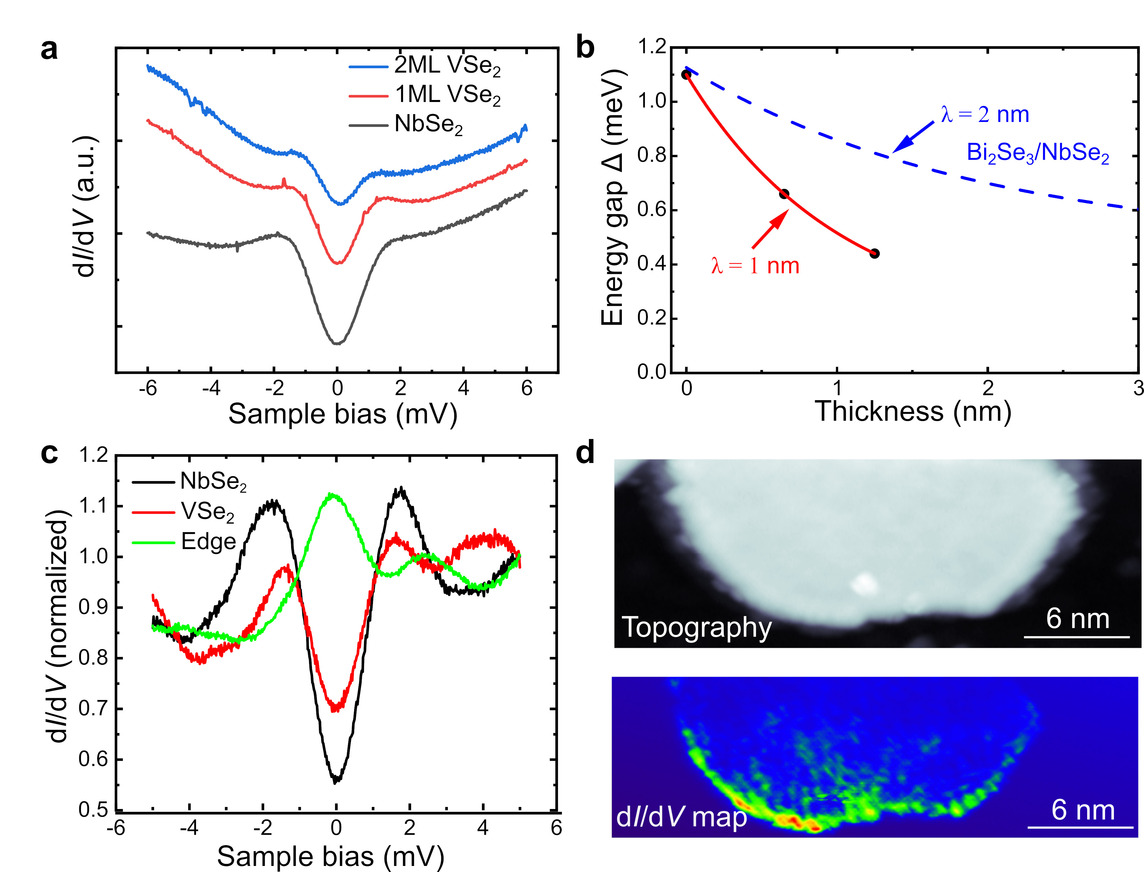
Fig. 5a shows the d/d spectra measured on the NbSe2 substrate as well as VSe2 layers with different thicknesses. On NbSe2, we observe a typical superconducting gap: a pronounced dip in the DOS at the Fermi level and coherence peaks on both sides of the gap58, 59. The spectra measured on the VSe2 films with thicknesses of 1 ML and 2 ML also shows a superconducting gap, but the gap width is significantly reduced compared to the bare NbSe2 substrate. We do not observe oscillatory behaviour of the pairing potential as bilayer VSe2 is not sufficiently thick for this. To further quantify the reduction of the SC gap width, we use a simple analytical relation between a superconducting gap and decay length 60, 61, 62: , where the is the VSe2 film thickness and is the gap of bare NbSe2, respectively. We extract the apparent gap widths from the spectra shown in Fig. 5a by fitting them (see SI Fig. S18 for details) and plot the results in Fig. 5b. The decrease of the energy gap follows an exponential dependence with an decay length of nm (1 ML thickness is roughly 0.65 nm). This is a measure of the quasi-particle coherence length associated with Andreev reflections. However, this decay length is much shorter than recent experimental results on Bi2Se3 on NbSe263: they observe a decay length of nm, which is shown as a dashed blue line in Fig. 5b. In the case of Bi2Se3 on Nb, an even much higher value of nm was reported62. The faster decay we observe in VSe2 is most easily explained by magnetism of the VSe2 layer. In this case, one would expect a shorter coherence length governed by the magnetization in the VSe2 layer and not by the diffusion (which is a case in Bi2Se3/NbSe2). The reduced gap is very uniform within the VSe2 islands and also between different islands. This shows that the observed response is not affected by the orientation of the VSe2 islands w.r.t. the underlying NbSe2 and that it is related to bulk properties of ML VSe2 and not simply an effect arising from impurities, vacancies, structural imperfections (e.g. layer edges).
We have also probed the spatially dependent spectroscopic response over the edges of the VSe2 islands and typical spectra are shown in Fig. 5c (more results in the SI Fig. S19). The spectra evolve from the typical gapped structure over the NbSe2 into a sharp peak at zero bias at the edge of the VSe2 island. This feature is very localized at the edge of the VSe2 layer. Furthermore, it is inhomogeneously distributed along the edges of VSe2 islands and there are strong intensity variations as illustrated in Fig. 5d. In addition to the spatial distribution of the zero bias peak, its width is also strongly position dependent. We observe both zero bias peaks that are confined within the superconducting gap (e.g. Fig. 5c), but on some other locations (see SI Fig. S19), its width can be a couple of times larger than the superconducting gap width. Features inside the superconducting gap could arise from Yu-Shiba-Rusinov bands or topological edge modes, but the broader peaks suggest the presence of free unpaired spins giving rise to the Kondo effect64, 21. In any case, the reason is likely related to the changes of the gap structure of the underlying superconductor due to local magnetic fields arising from the edges of the VSe2 layer. These results suggest importance of edge effects in the magnetism of the VSe2 layer.
Conclusions
In conclusion, we have demonstrated high-quality epitaxial growth of VSe2-NbSe2 hybrid structures using MBE. We have observed significant and spatially uniform reduction of the superconducting gap of the NbSe2 substrate on the VSe2 islands with the reduction being thickness dependent and stronger on bilayer VSe2. This would be most naturally explained to result from magnetization of the VSe2 layer. The other electronic and magnetic characterization results are also more consistent with magnetization than with charge density waves. Finally, we observe strongly position-dependent, enhanced d/d intensity at the Fermi level around the edges of the VSe2 layer suggesting that the atomic-scale structural details of the edge of monolayer VSe2 may contribute to its unusual magnetic response. Finally, our work suggests that it will be possible to combine 2D TMDs with different quantum ground states to stimulate new work in the field of 2D-TMDs hybrids.
2 Methods
Sample preparation. Monolayer VSe2 was grown on NbSe2 substrates by e-beam evaporation of V (99.8 %, Goodfellow Cambridge Ltd.) and simultaneous deposition of atomic Se (99.99 %, Sigma-Aldrich) from a Knudsen cell under ultra-high vacuum conditions (UHV, base pressure ). The NbSe2 substrate (HQ Graphene) was cleaved in vacuum and subsequently annealed in ultra-high vacuum at K for 1 h before film growth. VSe2 was grown at a substrate temperature of K. The growth was carried out under Se-rich conditions. The excess selenium desorbs from the substrate since the substrate temperature was higher than the evaporation temperature of selenium atoms ( K). The samples were either characterized in-situ by XPS and STM or capped with Se by deposition of Se at room temperature before transferring them out of the UHV system.
XPS measurements. XPS measurements (Surface Science Instruments SSX-100 spectrometer) were performed using monochromated Al K-alpha radiation with X-ray power of 200 W, a pass energy of 100 eV and a measurement spot size of 1 mm.
STM measurements. The STM experiments (Unisoku USM-1300) of the samples were performed at K. STM images were taken in the constant current mode. d/d spectra were recorded by standard lock-in detection while sweeping the sample bias in an open feedback loop configuration, with a peak-to-peak bias modulation of 5 mV (long-range spectra) or 0.1 mV (short-range spectra of the superconducting gap) at a frequency of 709 Hz.
Magnetic characterization. Magnetic characterization was carried out using a Quantum Design Dynacool PPMS operating as a vibrating sample magnetometer (VSM). For magnetization measurements the sample is attached to a quartz rod.
DFT calculations. All density-functional theory calculations are carried out in the plane-wave basis in the projector augmented wave framework as implemented in VASP 65, 66, 67. In all calculations, we use 500 eV cutoff and -point sampling corresponding to mesh in the primitive cell. High -point mesh is required to correctly describe e.g. the CDW phases. Further computational details are given in the SI.
V tends to exhibit strong Coulomb correlations, which usually necessitates using either hybrid functionals or +U. It was shown in Ref. 43, that depending on the U-parameter, the monolayer is either in nonmagnetic CDW state or in ferromagnetic no-CDW state. This balance is also affected by the number of electrons 43 and likely also by strain. Further details on the computational results on the interplay between magnetism and CDW stability is given in the SI.
This research made use of the Aalto Nanomicroscopy Center (Aalto NMC) facilities and was supported by the European Research Council (ERC-2017-AdG no. 788185 “Artificial Designer Materials”) and Academy of Finland (Academy professor funding no. 318995 and 320555, Academy postdoctoral researcher no. 309975, and Academy research fellow no. 311058). Our DFT calculations were performed using computer resources within the Aalto University School of Science “Science-IT” project and the Finnish CSC-IT Center for Science. M.M.U. acknowledges support by the Spanish MINECO under grant no. MAT2017-82074-ERC and by the ERC Starting grant LINKSPM (Grant 758558).
The Supporting Information is available free of charge on the ACS Publications website.
-
•
Computational details.
-
•
Further magnetization, XPS and STM experiments.
-
•
Effect of the substrate temperature on vanadium intercalation during VSe2 growth.
References
- Gomes et al. 2012 Gomes, K. K.; Mar, W.; Ko, W.; Guinea, F.; Manoharan, H. C. Designer Dirac Fermions and Topological Phases in Molecular Graphene. Nature 2012, 483, 306–310
- Slot et al. 2017 Slot, M. R.; Gardenier, T. S.; Jacobse, P. H.; van Miert, G. C. P.; Kempkes, S. N.; Zevenhuizen, S. J. M.; Smith, C. M.; Vanmaekelbergh, D.; Swart, I. Experimental Realization and Characterization of an Electronic Lieb Lattice. Nat. Phys. 2017, 13, 672–676
- Drost et al. 2017 Drost, R.; Ojanen, T.; Harju, A.; Liljeroth, P. Topological States in Engineered Atomic Lattices. Nat. Phys. 2017, 13, 668–671
- Khajetoorians et al. 2019 Khajetoorians, A. A.; Wegner, D.; Otte, A. F.; Swart, I. Creating Designer Quantum States of Matter Atom-by-Atom. Nat. Rev. Phys. 2019,
- Yan and Liljeroth 2019 Yan, L.; Liljeroth, P. Engineered Electronic States in Atomically Precise Artificial Lattices and Graphene Nanoribbons. Adv. Phys. X 2019, 4, 1651672
- Talirz et al. 2016 Talirz, L.; Ruffieux, P.; Fasel, R. On-Surface Synthesis of Atomically Precise Graphene Nanoribbons. Adv. Mater. 2016, 28, 6222–6231
- Gröning et al. 2018 Gröning, O.; Wang, S.; Yao, X.; Pignedoli, C. A.; Borin Barin, G.; Daniels, C.; Cupo, A.; Meunier, V.; Feng, X.; Narita, A.; Müllen, K.; Ruffieux, P.; Fasel, R. Engineering of Robust Topological Quantum Phases in Graphene Nanoribbons. Nature 2018, 560, 209–213
- Rizzo et al. 2018 Rizzo, D. J.; Veber, G.; Cao, T.; Bronner, C.; Chen, T.; Zhao, F.; Rodriguez, H.; Louie, S. G.; Crommie, M. F.; Fischer, F. R. Topological Band Engineering of Graphene Nanoribbons. Nature 2018, 560, 204–208
- Geim and Grigorieva 2013 Geim, A. K.; Grigorieva, I. V. Van Der Waals Heterostructures. Nature 2013, 499, 419
- Novoselov et al. 2016 Novoselov, K. S.; Mishchenko, A.; Carvalho, A.; Castro Neto, A. H. 2D Materials and Van Der Waals Heterostructures. Science 2016, 353, aac9439
- Huang et al. 2017 Huang, B.; Clark, G.; Navarro-Moratalla, E.; Klein, D. R.; Cheng, R.; Seyler, K. L.; Zhong, D.; Schmidgall, E.; McGuire, M. A.; Cobden, D. H.; Yao, W.; Xiao, D.; Jarillo-Herrero, P.; Xu, X. Layer-Dependent Ferromagnetism in a Van Der Waals Crystal Down to the Monolayer Limit. Nature 2017, 546, 270
- Gong et al. 2017 Gong, C.; Li, L.; Li, Z.; Ji, H.; Stern, A.; Xia, Y.; Cao, T.; Bao, W.; Wang, C.; Wang, Y.; Qiu, Z. Q.; Cava, R. J.; Louie, S. G.; Xia, J.; Zhang, X. Discovery of Intrinsic Ferromagnetism in Two-Dimensional Van Der Waals Crystals. Nature 2017, 546, 265–269
- Bonilla et al. 2018 Bonilla, M.; Kolekar, S.; Ma, Y.; Diaz, H. C.; Kalappattil, V.; Das, R.; Eggers, T.; Gutierrez, H. R.; Phan, M.-H.; Batzill, M. Strong Room-Temperature Ferromagnetism in VSe2 Monolayers on Van Der Waals Substrates. Nat. Nanotechnol. 2018, 13, 289–293
- Cao et al. 2018 Cao, Y.; Fatemi, V.; Fang, S.; Watanabe, K.; Taniguchi, T.; Kaxiras, E.; Jarillo-Herrero, P. Unconventional Superconductivity in Magic-Angle Graphene Superlattices. Nature 2018, 556, 43–50
- Gibertini et al. 2019 Gibertini, M.; Koperski, M.; Morpurgo, A. F.; Novoselov, K. S. Magnetic 2D Materials and Heterostructures. Nat. Nanotechnol. 2019, 14, 408–419
- Qi and Zhang 2011 Qi, X.-L.; Zhang, S.-C. Topological Insulators and Superconductors. Rev. Mod. Phys. 2011, 83, 1057–1110
- Mourik et al. 2012 Mourik, V.; Zuo, K.; Frolov, S. M.; Plissard, S. R.; Bakkers, E. P. A. M.; Kouwenhoven, L. P. Signatures of Majorana Fermions in Hybrid Superconductor-Semiconductor Nanowire Devices. Science 2012, 336, 1003–1007
- Nadj-Perge et al. 2014 Nadj-Perge, S.; Drozdov, I. K.; Li, J.; Chen, H.; Jeon, S.; Seo, J.; MacDonald, A. H.; Bernevig, B. A.; Yazdani, A. Observation of Majorana Fermions in Ferromagnetic Atomic Chains on a Superconductor. Science 2014, 346, 602
- Sato and Ando 2017 Sato, M.; Ando, Y. Topological Superconductors: a Review. Rep. Prog. Phys. 2017, 80, 076501
- Zhou et al. 2019 Zhou, J.; Qiao, J.; Duan, C.-G.; Bournel, A.; Wang, K. L.; Zhao, W. Large Tunneling Magnetoresistance in VSe2/MoS2 Magnetic Tunnel Junction. ACS Appl. Mater. Interfaces 2019, 11, 17647–17653
- Heinrich et al. 2018 Heinrich, B. W.; Pascual, J. I.; Franke, K. J. Single Magnetic Adsorbates on s-Wave Superconductors. Prog. Surf. Sci. 2018, 93, 1 – 19
- Pöyhönen et al. 2014 Pöyhönen, K.; Westström, A.; Röntynen, J.; Ojanen, T. Majorana States in Helical Shiba Chains and Ladders. Phys. Rev. B 2014, 89, 115109
- Kim et al. 2018 Kim, H.; Palacio-Morales, A.; Posske, T.; Rózsa, L.; Palotás, K.; Szunyogh, L.; Thorwart, M.; Wiesendanger, R. Toward Tailoring Majorana Bound states in Artificially Constructed Magnetic Atom Chains on Elemental Superconductors. Sci. Adv. 2018, 4, eaar5251
- Röntynen and Ojanen 2015 Röntynen, J.; Ojanen, T. Topological Superconductivity and High Chern Numbers in 2D Ferromagnetic Shiba Lattices. Phys. Rev. Lett. 2015, 114, 236803
- Li et al. 2016 Li, J.; Neupert, T.; Wang, Z.; MacDonald, A. H.; Yazdani, A.; Bernevig, B. A. Two-dimensional Chiral Topological Superconductivity in Shiba Lattices. Nat. Commun. 2016, 7, 12297
- Rachel et al. 2017 Rachel, S.; Mascot, E.; Cocklin, S.; Vojta, M.; Morr, D. K. Quantized Charge Transport in Chiral Majorana Edge Modes. Phys. Rev. B 2017, 96, 205131
- Nayak et al. 2008 Nayak, C.; Simon, S. H.; Stern, A.; Freedman, M.; Das Sarma, S. Non-Abelian Anyons and Topological Quantum Computation. Rev. Mod. Phys. 2008, 80, 1083–1159
- Alicea 2012 Alicea, J. New Directions in the Pursuit of Majorana Fermions in Solid State Systems. Rep. Prog. Phys. 2012, 75, 076501
- Wilczek 2009 Wilczek, F. Majorana Returns. Nat. Phys. 2009, 5, 614
- Ruby et al. 2015 Ruby, M.; Pientka, F.; Peng, Y.; von Oppen, F.; Heinrich, B. W.; Franke, K. J. End States and Subgap Structure in Proximity-Coupled Chains of Magnetic Adatoms. Phys. Rev. Lett. 2015, 115, 197204
- Ménard et al. 2017 Ménard, G. C.; Guissart, S.; Brun, C.; Leriche, R. T.; Trif, M.; Debontridder, F.; Demaille, D.; Roditchev, D.; Simon, P.; Cren, T. Two-Dimensional Topological Superconductivity in Pb/Co/Si(111). Nat. Commun. 2017, 8, 2040
- Palacio-Morales et al. 2019 Palacio-Morales, A.; Mascot, E.; Cocklin, S.; Kim, H.; Rachel, S.; Morr, D. K.; Wiesendanger, R. Atomic-Scale Interface Engineering of Majorana Edge Modes in a 2D Magnet-Superconductor Hybrid System. Sci. Adv. 2019, 5, eaav6600
- Liu et al. 2017 Liu, S.; Yuan, X.; Zou, Y.; Sheng, Y.; Huang, C.; Zhang, E.; Ling, J.; Liu, Y.; Wang, W.; Zhang, C.; Zou, J.; Wang, K.; Xiu, F. Wafer-Scale Two-Dimensional Ferromagnetic Fe3GeTe2 Thin Films Grown by Molecular Beam Epitaxy. npj 2D Mater. Appl. 2017, 1, 30
- Chen et al. 2019 Chen, W.; Sun, Z.; Gu, L.; Xu, X.; Wu, S.; Gao, C. Direct Observation of Van Der Waals Stacking Dependent Interlayer Magnetism. 2019, arXiv:1906.03383
- Feng et al. 2018 Feng, J.; Biswas, D.; Rajan, A.; Watson, M. D.; Mazzola, F.; Clark, O. J.; Underwood, K.; Marković, I.; McLaren, M.; Hunter, A.; Burn, D. M.; Duffy, L. B.; Barua, S.; Balakrishnan, G.; Bertran, F.; Le Fèvre, P.; Kim, T. K.; van der Laan, G.; Hesjedal, T.; Wahl, P. et al. Electronic Structure and Enhanced Charge-Density Wave Order of Monolayer VSe2. Nano Lett. 2018, 18, 4493–4499
- Wong et al. 2019 Wong, P. K. J.; Zhang, W.; Bussolotti, F.; Yin, X.; Herng, T. S.; Zhang, L.; Huang, Y. L.; Vinai, G.; Krishnamurthi, S.; Bukhvalov, D. W.; Zheng, Y. J.; Chua, R.; N’Diaye, A. T.; Morton, S. A.; Yang, C.-Y.; Ou Yang, K.-H.; Torelli, P.; Chen, W.; Goh, K. E. J.; Ding, J. et al. Evidence of Spin Frustration in a Vanadium Diselenide Monolayer Magnet. Adv. Mater. 2019, 31, 1901185
- Chen et al. 2018 Chen, P.; Pai, W. W.; Chan, Y.-H.; Madhavan, V.; Chou, M. Y.; Mo, S.-K.; Fedorov, A.-V.; Chiang, T.-C. Unique Gap Structure and Symmetry of the Charge Density Wave in Single-Layer . Phys. Rev. Lett. 2018, 121, 196402
- Duvjir et al. 2018 Duvjir, G.; Choi, B. K.; Jang, I.; Ulstrup, S.; Kang, S.; Thi Ly, T.; Kim, S.; Choi, Y. H.; Jozwiak, C.; Bostwick, A.; Rotenberg, E.; Park, J.-G.; Sankar, R.; Kim, K.-S.; Kim, J.; Chang, Y. J. Emergence of a Metal-Insulator Transition and High-Temperature Charge-Density Waves in VSe2 at the Monolayer Limit. Nano Lett. 2018, 18, 5432–5438
- Coelho et al. 2019 Coelho, P. M.; Nguyen Cong, K.; Bonilla, M.; Kolekar, S.; Phan, M.-H.; Avila, J.; Asensio, M. C.; Oleynik, I. I.; Batzill, M. Charge Density Wave State Suppresses Ferromagnetic Ordering in VSe2 Monolayers. J. Phys. Chem. C 2019, 123, 14089–14096
- Yu et al. 2019 Yu, W.; Lu, J.; Herng, T. S.; Wang, Z.; Zhao, X.; Chi, X.; Fu, W.; Abdelwahab, I.; Zhou, J.; Dan, J.; Chen, Z.; Chen, Z.; Li, Z.; Lu, J.; Pennycook, S. J.; Feng, Y. P.; Ding, J.; Loh, K. P. Chemically Exfoliated VSe2 Monolayers with Room-Temperature Ferromagnetism. Adv. Mater. 2019, 31, 1903779
- Sugawara et al. 2019 Sugawara, K.; Nakata, Y.; Fujii, K.; Nakayama, K.; Souma, S.; Takahashi, T.; Sato, T. Monolayer : Incommensurate Fermi Surface Nesting and Suppression of Charge Density Waves. Phys. Rev. B 2019, 99, 241404
- 42 Kim, T. J.; Ryee, S.; Han, M. J.; Choi, S. Sub-Room Temperature Ferromagnetism and Its Nature in VSe2 Monolayer. arXiv:1907.04790
- Fumega et al. 2019 Fumega, A. O.; Gobbi, M.; Dreher, P.; Wan, W.; González-Orellana, C.; Peña-Díaz, M.; Rogero, C.; Herrero-Martín, J.; Gargiani, P.; Ilin, M.; Ugeda, M. M.; Pardo, V.; Blanco-Canosa, S. Absence of Ferromagnetism in VSe2 Caused by Its Charge Density Wave Phase. J. Phys. Chem. C 2019, doi:10.1021/acs.jpcc.9b08868
- Bayard and Sienko 1976 Bayard, M.; Sienko, M. J. Anomalous Electrical and Magnetic Properties of Vanadium Diselenide. J. Solid State Chem. 1976, 19, 325–329
- Liu et al. 2018 Liu, Z.-L.; Wu, X.; Shao, Y.; Qi, J.; Cao, Y.; Huang, L.; Liu, C.; Wang, J.-O.; Zheng, Q.; Zhu, Z.-L.; Ibrahim, K.; Wang, Y.-L.; Gao, H.-J. Epitaxially Grown Monolayer VSe2: an Air-Stable Magnetic Two-Dimensional Material with Low Work Function at Edges. Sci. Bull. 2018, 63, 419–425
- Wang et al. 2017 Wang, H.; Huang, X.; Lin, J.; Cui, J.; Chen, Y.; Zhu, C.; Liu, F.; Zeng, Q.; Zhou, J.; Yu, P.; Wang, X.; He, H.; Tsang, S. H.; Gao, W.; Suenaga, K.; Ma, F.; Yang, C.; Lu, L.; Yu, T.; Teo, E. H. T. et al. High-quality Monolayer Superconductor NbSe2 Grown by Chemical Vapour Deposition. Nat. Commun. 2017, 8, 394
- Arguello et al. 2014 Arguello, C. J.; Chockalingam, S. P.; Rosenthal, E. P.; Zhao, L.; Gutiérrez, C.; Kang, J. H.; Chung, W. C.; Fernandes, R. M.; Jia, S.; Millis, A. J.; Cava, R. J.; Pasupathy, A. N. Visualizing the Charge Density Wave Transition in - in Real Space. Phys. Rev. B 2014, 89, 235115
- Ma et al. 2012 Ma, Y.; Dai, Y.; Guo, M.; Niu, C.; Zhu, Y.; Huang, B. Evidence of the Existence of Magnetism in Pristine VX2 Monolayers (X = S, Se) and Their Strain-Induced Tunable Magnetic Properties. ACS Nano 2012, 6, 1695–1701
- Coey et al. 2016 Coey, J. M. D.; Venkatesan, M.; Stamenov, P. Surface Magnetism of Strontium Titanate. J. Phys.: Condens. Matter 2016, 28, 485001
- Coey 2019 Coey, J. M. D. Magnetism in d0 Oxides. Nat. Mater. 2019, 18, 652–656
- del Valle et al. 2017 del Valle, J.; Gomez, A.; Gonzalez, E. M.; Manas-Valero, S.; Coronado, E.; Vicent, J. L. Force-free State in a Superconducting Single Crystal and Angle-Dependent Vortex Helical Instability. Phys. Rev. B 2017, 95, 224510
- Galvan et al. 2003 Galvan, D. H.; Li, S.; Yuhasz, W. M.; Kim, J.; Maple, M. B.; Adem, E. Superconductivity of NbSe2 Samples Subjected to Electron Irradiation. Physica C 2003, 398, 147–151
- Naik et al. 2013 Naik, I.; Tiwari, G. C.; Yadav, C. S.; Rastogi, A. K. Effect of Magnetic Exchange Interaction in Resistivity on -Nb1-xVxSe2. Indian J. Phys. 2013, 87, 1075–1078
- Pervin et al. 2017 Pervin, R.; Krishnan, M.; Rana, A. K.; Kannan, M.; Arumugam, S.; Shirage, P. M. Enhancement of Superconducting Critical Current Density by Fe Impurity Substitution in NbSe2 Single Crystals and the Vortex Pinning Mechanism. Phys. Chem. Chem. Phys. 2017, 19, 11230–11238
- Chatterjee et al. 2015 Chatterjee, U.; Zhao, J.; Iavarone, M.; Di Capua, R.; Castellan, J. P.; Karapetrov, G.; Malliakas, C. D.; Kanatzidis, M. G.; Claus, H.; Ruff, J. P. C.; Weber, F.; van Wezel, J.; Campuzano, J. C.; Osborn, R.; Randeria, M.; Trivedi, N.; Norman, M. R.; Rosenkranz, S. Emergence of Coherence in the Charge-Density Wave State of -NbSe2. Nat. Commun. 2015, 6, 6313
- Linder and Robinson 2015 Linder, J.; Robinson, J. W. A. Superconducting spintronics. Nat. Phys. 2015, 11, 307
- Buzdin 2005 Buzdin, A. I. Proximity Effects in Superconductor-Ferromagnet Heterostructures. Rev. Mod. Phys. 2005, 77, 935–976
- Hudson 1999 Hudson, E. W. Investigating High-Tc Superconductivity on the Atomic Scale by Scanning Tunneling Microscopy; Ph.D. Thesis, University of California, Berkeley, 1999
- Noat et al. 2015 Noat, Y.; Silva-Guillén, J. A.; Cren, T.; Cherkez, V.; Brun, C.; Pons, S.; Debontridder, F.; Roditchev, D.; Sacks, W.; Cario, L.; Ordejón, P.; García, A.; Canadell, E. Quasiparticle Spectra of : Two-Band Superconductivity and the Role of Tunneling Selectivity. Phys. Rev. B 2015, 92, 134510
- Reeg and Maslov 2016 Reeg, C. R.; Maslov, D. L. Hard Gap in a Normal Layer Coupled to a Superconductor. Phys. Rev. B 2016, 94, 020501
- Belzig et al. 1996 Belzig, W.; Bruder, C.; Schön, G. Local Density of States in a Dirty Normal Metal Connected to a Superconductor. Phys. Rev. B 1996, 54, 9443–9448
- Flötotto et al. 2018 Flötotto, D.; Ota, Y.; Bai, Y.; Zhang, C.; Okazaki, K.; Tsuzuki, A.; Hashimoto, T.; Eckstein, J. N.; Shin, S.; Chiang, T.-C. Superconducting Pairing of Topological Surface States in Bismuth Selenide Films on Niobium. Sci. Adv. 2018, 4, eaar7214
- Wang et al. 2012 Wang, M.-X.; Liu, C.; Xu, J.-P.; Yang, F.; Miao, L.; Yao, M.-Y.; Gao, C. L.; Shen, C.; Ma, X.; Chen, X.; Xu, Z.-A.; Liu, Y.; Zhang, S.-C.; Qian, D.; Jia, J.-F.; Xue, Q.-K. The Coexistence of Superconductivity and Topological Order in the Bi2Se3 Thin Films. Science 2012, 336, 52
- Franke et al. 2011 Franke, K. J.; Schulze, G.; Pascual, J. I. Competition of Superconducting Phenomena and Kondo Screening at the Nanoscale. Science 2011, 332, 940–944
- Kresse and Hafner 1993 Kresse, G.; Hafner, J. Ab Initio Molecular Dynamics for Liquid Metals. Phys. Rev. B 1993, 47, 558–561
- Kresse and Furthmüller 1996 Kresse, G.; Furthmüller, J. Efficiency of Ab-Initio Total Energy Calculations for Metals and Semiconductors Using a Plane-Wave Basis Set. Comp. Mat. Sci. 1996, 6, 15–50
- Blöchl 1994 Blöchl, P. E. Projector Augmented-Wave Method. Phys. Rev. B 1994, 50, 17953–17979