Nanoscale ballistic diodes made of polar materials for amplification and generation of radiation in 10 THz-range
Abstract
We investigate ultra-high frequency electrical properties of nanoscale diodes made of polar semiconductors. The calculations show that the coupling between optical vibrations of the lattice and the ballistic electrons strongly modifies and enhances the time-of-flight effects giving rise to narrow resonances of the diode impedance in the reststrahlen frequency range. Particularly, negative dynamic resistance is induced in close proximity to the optical phonon frequency. The resonant effects in the dynamic resistance of nanoscale GaAs and InP diodes are studied in detail. The obtained magnitudes of the negative dynamic resistance effect indicate that the nanoscale diodes are capable of generating electromagnetic radiation in far-infrared spectral range under electric pumping.
I Introduction
The interaction of ballistic electrons with the electromagnetic radiation offers a significant opportunity for generation and detection of ultra-high frequency radiation. Particularly, the two- and three-terminal structures scaled down to the nanometer dimensions can access the THz frequency range by taking advantage of the ultra-fast semiclassical ballistic electron transport. Dyak ; TWT-1 ; Ryzhii-1 ; Grib ; Grib-1 It is believed that nanoscale ballistic devices have already reached to the point where their basic effects and operational principles are very similar to those of the electron vacuum tubes exploiting the time-of-flight effects (see, for example, Ref Tubes, ). However, semiconductor materials possess a number of inherent properties different from the vacuum tubes. For example, the nonparabolic energy dispersion in the semiconductors can lead to the negative effective masses Grib and the velocity saturation Grib-1 at large electron energies, which drastically modify both steady state and high frequency parameters of the ballistic diodes.
Another important factor giving rise to characteristic features of solid-state ballistic devices is the frequency dependence of the dielectric permittivity . Indeed, the high frequency response of these devices and, particularly, the negative dynamic resistance (NDR) effect arise due to the correlation between the electronic motion and the space charge dynamics. Ryzhii-1 ; Grib ; Grib-1 ; JNO ; Firsov1 The latter are strongly influenced by the screening effects. Polarization of the crystal lattice also contributes to the screening. In the important case of polar materials, the lattice polarization via optical vibrations determines the dielectric permittivity as: Born
| (1) |
where and are the low frequency and high frequency permittivities, respectively, is the frequency of the transverse optical vibrations, and is the optical phonon damping. The frequency of the longitudinal optical vibrations, , equals to . The permittivity, , varies considerably near the frequency and can change its sign in the interval , which is known as the reststrahlen frequency range (RFR). Cardona ; Adachi
When in a diode, the electron time-of-flight, , is of the order of , one can expect resonant effects in high frequency resistivity. Physics-based explanation of expected effects is obvious. Under the mentioned condition, characteristic frequencies of ballistic charge transfer across the diode are in the resonance with the polarization lattice vibrations. This results in a sharp enhancement of mutual influence of the electron and polarization dynamics in the narrow RFR. In general, a time dependent perturbation of the voltage applied to the diode can be presented as a Fourier expansion with different frequencies. One can suppose that the Fourier components of the diode response (the current) to this perturbation with frequencies close to will be resonantly increased.
Note, for semiconductor materials and heterostructures widely used in high speed electronics, the characteristic frequencies of optical phonons vary in a wide THz range. In III-V compounds are in the range 5 THz (InSb) to 12 THz (GaP) Levinshtein ; for the group-III-nitrides are of 18 to 22 THz Adachi ; Firsov2 , etc. Currently, for this frequency range the physical effects are actively studied, Leit-1 ; Leit-2 ; Tsen-1 ; Jap ; PRL-2019 as well as their device applications. Gelmont ; Kim ; Shur ; Kukhtaruk ; Sydoruk ; Ohtani ; Khurgin-1 ; polaron-l-2
In this paper, we investigate ultra-high frequency electron response of nanoscale ballistic diodes. For the nanoscale structures made of a polar material, it is found that the polarization lattice vibrations provide the dynamic screening and contribute to the resonant high frequency response, leading to large effects in the resistivity and, particularly, to an enhanced NDR effect in the RFR. This mechanism can provide an electrical means to amplify and generate electromagnetic radiation in 10–THz frequency range, i.e., far-infrared radiation.
To study the resonant enhanced effects in the resistivity for the RFR, we analyze a short diode assuming ballistic electron motion and frequency dependent permittivity of Eq. (1) in the -region (). Two models of the electron transport are considered: the model of monoenergetic electron injection into the i–region (the base) and the model based on the Boltzmann transport equation for the injected electrons.
II Model of monoenergetic electron injection
We begin with the analysis of a simple model of the diode with injection of monoenergetic electrons from cathode to the base. This model facilitates the understanding of main features of the high-frequency electron dynamics and resistivity of the diode in the RFR. To describe the semiclassical space-charge-limited transport of ballistic electrons we introduce the velocity, , the electron density, , the electric field, , and the electron current density, . Here the coordinate varies along the diode base: . For this approach, the basic equations are the Newton’s law, the continuity equation, and the Poisson equation:
| (2) | |||
| (3) | |||
| (4) |
Here, is the electron effective mass and is the electric displacement. In Eqs. (2)-(4), every variable can be presented as a sum of steady state and time dependent contributions: , , etc. Then, one can define with and . The expression for is as provided in Eq. (1). The dynamic lattice polarization, , can be calculated via the alternative electric field :
| (5) |
From Eqs. (3) and (4), it follows that the sum of the conductivity current and the displacement current (i.e., the total current) is constant throughout the diode. This leads to and for the steady state and time dependent problems, respectively. With given and , both problems are reduced to determining two unknown functions, for example, and .
Below we use the ”virtual cathode approximation” virtual , correspondingly, we set (i.e., the initial velocity) and for the steady state problem, and for the time dependent case, respectively. We also assume that there is no reflection of the electrons from the anode comment-1 .
The steady state problem has a well-known solution in the implicit form:
| (6) | |||
| (7) |
with varying from to . The current-voltage characteristic is given in a parametric form:
| (8) | |||
| (9) |
where is the applied voltage and has the meaning of the electron velocity at the anode. At large biases, these formulae lead to the Child’s law: virtual
For the time-dependent problem, we obtain two linear differential equations:
| (10) | |||
| (11) |
An important property of these equations is the -dependencies of the coefficients via the steady state solution . To solve Eqs. (10), (11), it is convenient to introduce a dimensionless variable, , in place of :
as well as dimensionless functions in place of the electron velocity and the field :
| (12) | |||||
| (13) |
where
| (14) |
In such a formulation, the results are parametrically dependent on dimensionless applied voltage, , and initial velocity, ,:
| (15) |
Then, Eqs. (10) and (11) can be rewritten in a simpler form:
| (16) |
Here, only the second equation parametrically depends on frequency via the resonant factor and the oscillating exponential in the right hand side (rhs). The latter determines time-of-flight resonances of ballistic electrons at a given frequency and, particularly, the optical phonon - transit time resonance at . According to the above discussion, the boundary conditions for Eqs. (16) are . If and are found, coordinate dependencies and can be recovered by using Eqs. (12), (13) and the following relationships:
| (17) |
It is useful to indicate that maximum of the phase of the exponential in the rhs of the second Eq. (16) is:
| (18) |
where the time-of-flight, , is determined as
Eqs. (16) can be solved exactly in terms of the Legendre functions Legandre , and . Indeed, from the system of Eqs. (16) one can obtain a single second order differential equation,
| (19) |
Corresponding homogeneous equation has the following independent solutions:
Two independent solutions of a linear homogeneous second order differential equation allow one to construct a general solution to nonhomogeneous Eq. (19). The resulting expression for this solution is cumbersome and is not presented in this paper. Instead, we shall concentrate on the discussion of conclusions, which follow from this solution.
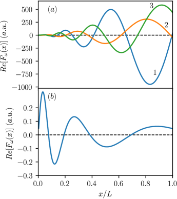
At the zero boundary conditions, the time-dependent variations of the velocity, , and the field, , are induced entirely by the external ac electric bias. By solving Eqs. (16), (19) for and , and using formulae (12), (13) and (17), we found that in the RFR the velocity and the field are critically dependent on the frequency. In Fig. 1 (a) we show ’snapshots’ of the field-coordinate dependencies for three frequencies close to at the same stationary current (voltage) and a given amplitude of the alternative current, , which is set a real and positive value. The fields are oscillating functions of with growing amplitudes along the electron flow. From Eq. (5) it follows that the lattice polarization, , behaves similarly to the alternative field, however, in the RFR it is opposite in phase. The effect of growing field amplitudes can be directly seen from Eq. (16), where parameter is negative in the RFR and both become large at (i.e., ). For comparison, in Fig. 1 (b) we present the ’snapshot’ of the field-coordinate dependency for the case, when the lattice polarization is neglected (). The assumed parameters of the diode and the currents and are the same as for Fig. 1 (a). It is seen, that the alternative field is still oscillating, but its amplitude decreases along the electron flow.
By using real and imaginary parts of and we found that spatio-temporal dependencies of the electron velocity and the electric field are in the form of waves propagating from the cathode to the anode; their amplitudes increase toward the anode.
Once the dependence is obtained, we can calculate the diode impedance (per unit area of the device cross-section) as
| (20) | |||
In Fig. 2, examples of the calculations of the diode impedance, , are shown. For this particular diode, we found ps, . In the main part of the figure (panel (c)), the real and imaginary parts of are presented for the narrow frequency interval near (). For the used parameters (see discussion below), the RFR is . In Fig. 2 (a), is shown for the magnified frequency interval, . In Fig. 2 (b), the same is shown for the case, when the dynamic polarization of the lattice is neglected, i.e., . For the latter case, the frequency dependence of is solely due to the time-of-flight effects (see, for example, Ref. Grib-1, ; JNO, ).
From presented results it follows that the lattice vibrations in polar materials give rise to strong modifications of the high-frequency resistivity in the RFR near the optical phonon frequency. Both and demonstrate a few oscillations with amplitudes tens time larger than the differential resistivity in the steady state regime, . Particularly, shows alternative inductive and capacitive characters, in opposite to the exclusively inductive character in the case of dispersionless permittivity shown in Fig. 2(b). While shows two narrow bands and with negative dynamic resistance, that reaches values at and at . The second very narrow bands is confined between two bands of positive dynamic resistances with sharp peaks at and at . For comparison, in the case of the dispersionless permittivity the NDR is predicted in the wide band, , but the amplitude of the effect is very small: .
The physics underlying the effects of positive and negative is related to correlation between the electronic motion and the self-consistent alternative field. This is well illustrated by the field-coordinate dependencies presented in Fig. 1. Indeed, during dynamic processes of a given frequency, , gain/loss of local electron energy is determined by the electrical power density averaged over the time period: . For Fig. 1 it was set as real and positive, thus for presented results . One can see that for all cases the power density is oscillating function on the coordinate. For curves of Fig. 1 (a) and for Fig. 1 (b) the total electric power transferred to the electrons (i.e., ) is positive, which corresponds to an absorption of high-frequency electrical power in the diode base (corresponding resistivity ). However, for curve 1 of Fig. 1 (a), the total power transferred to the electrons is evidently negative, which means gain of high-frequency electric power (corresponding resistivity ).
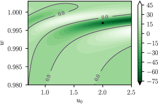
More general pattern of the resonances in the high-frequency resistivity of the short diode is illustrated in Fig. 3, where the density plot of is presented as a function of two variables: and . The thin lines mark regions with the NDR. The narrowness of these regions is explained by the resonance character of the discussed effects. These results demonstrate that the resonant character of the dielectric permittivity of Eq. (1) cardinally modifies the diode response in the RFR and leads to regions with the NDR.
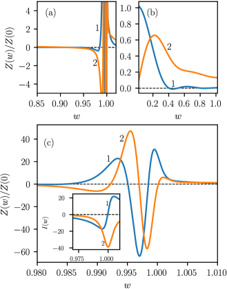
Generally, the diode response, , is strongly influenced by the two main factors entering Eqs. (16), (19). The first factor, , determines the coupling between the charge, its motion and the electrostatic field. In the narrow frequency interval near , this factor critically depends on both the dimensionless frequency, , and the dimensionless optical phonon damping, . The resonant character of the -dependence is illustrated in the Inset of Fig. 2 (c) for (the discussion of and is presented below). The minimum (m) and maximum (M) of are realized at , respectively. In the limit , at we find large negative values of :
| (21) |
In the above analyzed examples with very close frequencies corresponding to the maxima and minimum of , we obtain sufficiently different values of : , and . These result in distinct behavior of the high frequency fields and impedances, as shown in Figs. 1 and 2.
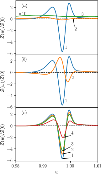
Fig. 4 (a) illustrates the large effect of the phonon damping, , on the resonance features of . At small value of the damping, , the amplitudes of the resonant variations of the high frequency resistivity are large. Twofold increase in leads to more than one order decreasing in these amplitudes. Subsequent twofold increase in totally suppress the resonance effects.
Note, according to Eq. (21) for frequencies near , the factor is proportional to , which characterizes a relative contribution of the polar lattice vibrations to the permittivity, as well as the electron-optical phonon coupling. RTD-1 Thus, materials with larger polar properties (larger ionicity) should show larger discussed effects.
The second factor influencing the studied resonant effects is the product given by Eq. (18). Since the major effects are expected at close to , this factor depends mainly on the diode length, , and the applied dc voltage, , via the -dependence.
It is necessary to mention that in the model of the monoenergetic electron injection the discussed results depend on the initial electron energy (velocity, ). Varying at fixed other parameters, we found that the resonance features in the resistivity are always observable, however, there are frequency shifts in their position. Fig. 4 (b) illustrates the effect of initial velocity on the resistivity, .
The above results were obtained for strictly collisionless motion of the electrons in the diode base. Approximately, the effect of electron scattering can be estimated by introducing a ”frictional force”, into the right hand side of the Newton Eq. (2), with being the electron scattering time. Accordingly, in the right hand side of the first equation from (16), we need to add the term . In Fig. 4 (c) we present calculated for different ratio at fixed other parameters. From these estimations it follows that though processes of electron scattering suppress the resonant effects in the high-frequency resistivity, the effects persist considerably large even at , i.e., for quasi-ballistic electron motion.Grib-1
III Examples of nanodiodes based on III-V compounds.
In this Section we consider the resonant effects in the high-frequency resistivity for a few particular nanodiodes based on polar III-V semiconductor compounds.
As discussed above, the value of the optical phonon damping, , is critically important for the resonant effects under consideration. Thus we shall begin with a remark about the available data on phonon decay. Two different approaches were used to study the optical phonon decay. The first is incoherent Raman spectroscopy of noncoherent nonequilibrium phonons based on time-resolved incoherent Raman measurements, Linde ; Kash or on measurements of the linewidth of spontaneous Raman scattering. Evans ; Paraya This approach provides experimental measurements of the time of relaxation of the phonon energy. The second approach uses the time-resolved coherent nonlinear technique (anti-Stokes Raman scattering). In such an approach, an optical phonon is excited coherently and the subsequent dynamics of its dephasing can be monitored. Vallee ; Bron As a result, the phonon dephasing time, , can be extracted. Namely, the latter parameter determines the value . For polar materials GaAs, InP, dephasing processes of the optical phonons and the time, has been studied and measured in detail. Vallee ; Bron
GaAs diodes. For numerical results presented in Figs. 1 - 3, we used the material parameters of GaAs: , , meV ( THz, ) and , where is the free electron mass. The assumed ballistic transport regime is valid if the mean free path of the electrons exceeds the diode length . The mean free path depends drastically on the electron energy. In a high quality intentionally undoped GaAs sample at the lattice temperature below K, the electrons with the energy less than have the mean free path up to m. The electrons with the energy above relax quickly through emission of optical phonons. Direct Monte-Carlo simulation of the dynamics of the injected electrons in GaAs at K proves that the fraction of the ballistic electrons at the distance nm equals 0.74 for . These values of and are used in calculations presented in Figs, 1 - 3 . The relevant steady state electrical characteristics are: the current density kA/cm2 and cm2. For Figs. 1 - 3 and 4 (a), (c), initial velocity of the injected electrons is set , which corresponds to the electrons injected from a cathode at K, while corresponds to the electrons injected at K (Fig. 4 (b), curve 2). The latter results indicate a considerable dependence of the resonances on initial velocity of injected electrons: particularly, the frequency bands of the NDR are shifted and amplitudes of the effects are changed.
For high quality GaAs crystals, it was found the optical phonon dephasing times: ps at K, ps at K, ps at K. Vallee Corresponding phonon damping parameter is , In the model calculations presented in Figs. 1 - 3 we used .
For comparison ballistic and quasi-ballistic diodes, which is shown in Fig. 4 (c), we used the scattering times, , corresponding to following values of the mobility: cm2/(Vs), curves , respectively.
We performed also the calculations for the GaAs diode with shorter base, nm, for which the fraction of the ballistic electrons exceeds and at and , respectively. For such a diode, at we found kA/cm2, the windows with the NDR, , and cm2 at . At , we obtained kA/cm2 and cm2 at .
InP diodes. In comparison with GaAs, InP crystals are characterized larger ionicity (see Eq. 21) and larger optical phonon lifetime. For calculations we used the following parameters of InP: , , meV ( THz, ) and . In high-quality InP crystals at low temperatures ( K) the electron mobility can reach cm2/Vs, with the mean free path up to m. However, the electrons with energies above rapidly emit the optical phonons, (this is actual for ). We found that the fractions of the ballistic electrons at the distance nm are greater than 0.95 and 0.6 for and , respectively. At the distance nm and , the fraction of the ballistic electrons is . Thus, for these parameters the electron transport can be considered as quasi-ballistic.
InP materials are characterized by relatively large optical phonon lifetime: ps at K (), ps at K () and ps at K ().Vallee ; gamma-1 In the model calculations presented below we used .
We found that nanoscale InP-diodes show all discussed above resonant features of the resistivity near the optical phonon frequency. In the case of the base length nm at we found ps, , kA/cm2, cm2. There is one relatively wide frequency interval with NDR, , where cm2 at .
In the case of the base length nm at we found ps, , kA/cm2, cm2. There is one frequency interval with NDR, , with cm2 at . In general, the analyzed resonant effects are considerable larger for nanoscale InP-based diodes in comparison with the GaAs diodes.
Thus, the model of the monoenergetic electron injection predicts strong resonant effects in high-frequency resistivity and opening frequency windows with large amplitudes of the NDR. Finalizing this analysis we mention that this type of the injection can be realized, for example, by the use of the resonant tunneling through a double barrier heterostructure. RTD-1 Indeed, at the resonant tunneling the spread of the energy of injected electrons can be less or order of meV, while the current densities reach tens to hundred of kA/cm2. RTD-1
For more common contacts, the injected electrons are spread over energy according to the temperature of the cathode. Different groups of the electrons are injected with different velocities, are characterized by different times of flight and contribute to the resistivity resonances at slightly different frequencies. Consequently, the overall resonance effects decrease.
To take into account the finite temperature of the injected electrons we should apply more adequate model for the ballistic electron transport in the nanodiodes.
IV Model based on Boltzmann transport equation for injected ballistic electrons.
To take into account the velocity distribution of the injected electrons, Eqs. (2) and (3) should be replaced by the Boltzmann equation for the distribution function . In the case of the ballistic electrons, the latter equation reads:
| (22) |
Now two functions, and , describe completely the system under consideration. The electron concentration and the current can be calculated by using : i.e., . The latter relationships and Eqs. (1), (4), (22) comprise the necessary set of the equations. The boundary condition to Eq. (22) is determined by the equilibrium distribution of the incoming electrons at a given temperature of the cathode. As described earlier, we separate the steady state and time-dependent problems: and . While the steady state solutions and can be found analytically (see, for example, Ref. Bulashenko, ), the time dependent solutions require the use of numerical calculations, as discussed in Ref. JNO, .
The subsequent computations confirmed the basic conclusions discussed in Sections II and III for the simple model. We also checked that the results based on the Boltzmann transport coincide with those obtained in the simple model, when the cathode temperature . At a finite temperature, , we found that current-voltage characteristics and are almost the same as in the simplest model. However the resonance effects are weakened, as expected.
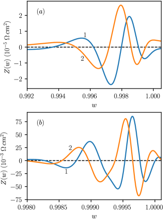
In Fig. 5 (a), we present for the nm GaAs diode at the cathode temperature K assuming meV () and restricting ourselves to the case of a small dephasing optical phonon lifetime, ps. We can see that there are two frequency bands with the pronounced resonances and the NDR: with cm2 at and with cm2 at . Further increase in suppresses the resonant effects, for example, at K we found only one frequency band with the NDR: and cm2 at .
Similar results we obtained for the nm GaAs diodes at K and K under the voltage meV. For example, at K and meV we found cm2.
In Fig. 5 (b), calculations of for the nm InP diode are shown at the cathode temperature K and meV() and the dephasing optical phonon lifetime ps. We found three very narrow frequency bands with the NDR near : with cm2 at ; with cm2 at ; with cm2 at . We found that the resonant effects under consideration remain at elevated temperatures. For example, at K and two most pronounced frequency bands with the NDR were obtained as with cm2 at , and with cm2.
Note, for both GaAs and InP diodes we used small dephasing optical phonon times ( ps and ps, respectively). In high quality materials can be two to three times larger, thus the amplitude of the NDR can be increased by one order of value.
V Discussion and summary
We investigated ultra-high frequency electron response of nanoscale ballistic diodes made by polar materials. For such nanoscale diodes the polarization lattice vibrations provide the dynamic screening and significantly contribute to the high frequency response of the devices. When characteristic frequencies of ballistic electron transfer across the diode are of the order of the polarization lattice vibrations, we found large resonant effects in the frequency dependent resistivity and an enhanced negative dynamic resistivity in the reststrahlen frequency range.
In this frequency range, as the result of the specific dynamic screening, the alternative self-consistent electric field, the lattice polarization and the electron (average) velocity are oscillating functions of the coordinate with growing amplitudes along the electron flow. While outside of the RFR amplitudes of these characteristics decrease along the flow. In close proximity to the optical phonon frequency both real and imaginary parts of the impedance show a few oscillations with amplitudes tens time larger than the differential resistivity in the steady state regime, . Particularly, shows alternative inductive and capacitive characters, in opposite to the exclusively inductive character in the case, when the dynamic lattice polarization is neglected (see Fig. 1 (b)). While becomes negative, generally, in several very narrow frequency bands (of order of cm-1 (InP) … cm-1 (GaAs) in conventional units).
The amplitudes and sharpness of the resonances are determined by the factor (21), which is proportional to both a relative contribution of the polar lattice vibrations to the permittivity and the optical phonon lifetime. Comparison of the diodes made of GaAs (the material with modest polar properties and a small optical phonon lifetime) and InP (the material with larger ionicity and larger phonon lifetime) demonstrates that the latter diodes should show considerably stronger resonant effects in the dynamic resistivity.
It was ascertained that in the ballistic diodes the studied effects are dependent on the temperature of the electrons injected from the cathode: an increase in the cathode temperature suppresses the resonant effects. Meanwhile, the resonant effects, including the negative resistance in the RFR, are still pronounced at K for the GaAs diodes and at K for the InP diodes.
The studied NDR of the nanoscale diodes can be utilized to amplify and generate far-infrared emission at the expanse of energy of the current. Indeed, absolute values of found specific negative dynamic resistance, above cm2 for the GaAs diodes and above cm2 for the InP diodes, are well above the specific contact resistances for these materials ( cm2). contacts Thus the necessary condition of negative resistance of whole device TWT-1 with contacts can be met. The current densities are estimated to be of the order of tens of kA/cm2. Then, gain and threshold of electromagnetic generation are determined by the active part of the diode admittance (conductance), with . The key parameter of a device is its quality factor . Value nearly is favorable for easy matching to external circuits. TWT-1 ; Grib-1 As seen from Figs. 5 in every spectral band with the NDR there is a frequency for which the latter requirement is met for both GaAs and InP diodes. Absolute values of are sufficient to provide an electrical means to amplify and generate electromagnetic radiation in far-infrared spectral range.
The ultra-high frequency resonances and NDR also can be observed in planar nanoscale diodes made from hybrid structures - non-polar semiconducting films or two-dimensional crystals on polar substrates. Indeed, in such structures time- and space-dependent planar electron transport induces an alternative electric fields, which, in turn, polarize substrate near the interface. As a result, one can expect resonant interaction of electron flux with polarized substrate near surface optical phonon frequencies. Examples are graphene on polar substrates (, etc.). Different aspects of interaction of graphene electrons with polar substrates were studied in numerous papers (see, for example, int-1 ; int-2 ; int-3 ; int-4 ). High mobilities in these structures facilitate ballistic electron transport over large length scales (hundreds ) graph-1 ; graph-2 ; graph-3 . These properties are favorable for observation of ultra-high frequency resonances in resistivity of planar nanoscale diodes based on the hybrid structures, however discussed effects require additional analysis.
In summary, nanoscale diodes made of a polar material with ballistic electron transport can exhibit a large effect of optical lattice vibrations on the ultra-high frequency electrical properties of the diodes. This results in the modification of the time-of-flight effects and dramatic reconstruction of the -dependent impedence/admittance in the reststrahlen frequency range. Particularly, narrow resonances in the diode impedance with the negative real part are induced near the optical phonon frequency. The resonant effects in the dynamic resistance of nanoscale GaAs and InP diodes are studied in detail. The obtained magnitudes of the NDR effect indicate that the nanoscale diodes are capable to amplify and generate electromagnetic radiation in the 10-THz range.
Acknowledgements.
The authors are grateful to Dr. G. I. Singayivska for estimations of the electron ballisticity under high applied voltage. This work was supported by Science & Technology Center in Ukraine (STCU-NASU TRI project #3922 ”New Technologies of THz and sub-THz Generation with Nanosize Semiconductor Heterostructures”)References
- (1) M. Dyakonov and M. Shur, Phys. Rev. Lett. 71, 2465 (1993); F. J. Crown, J. Appl. Phys. 87, 8056 (2000); W. Knap, J. Rusakowski, T. Parenty, S. Bollaert, A. Cappy, V. V. Popov, and M. S. Shur, Appl. Phys. Lett. 84, 2331 (2004); J. Lusakowski, W. Knap, N. Dyakonova, L. Varani, J. Mateos, T. Gonzalez, Y. Roelens, S. Bollaert, A. Cappy, and K. Karpierz, J. Appl. Phys. 97, 064307 (2005).
- (2) G. I. Haddad, J. R. East, and H. Eisele, Intl. J. High Speed Electron. Systems 13, 45 (2003).
- (3) V. I. Ryzhii, N. A. Banov, and V. A. Fedirko, Sov. Phys. Semicond. 18, 769 (1984).
- (4) Z. S. Gribnikov, A. N. Korshak, and V. V. Mitin, Int. J. Infrared Millimeter Waves 20, 213 (1999); Z. S. Gribnikov, N. Z. Vagidov, and V. V. Mitin J. Appl. Phys. 88, 6736 (2000).
- (5) Z. S. Gribnikov, N. Z. Vagidov, V. V. Mitin, and G. I. Haddad, J. Appl. Phys. 93, 5435 (2003); Z. S. Gribnikov, N. Z. Vagidov, and G. I. Haddad, ibid 95, 1489 (2004).
- (6) W. E. Benham, Phil. Mag. 11, 457 (1931); F. B. Llewellyn and A. E. Bowen, Bell Syst. Tech. J. 18, 280 (1939).
- (7) V. V. Korotyeyev, V. A. Kochelap, A. A. Klimov, G. Sabatini, H. Marinchio, C. Palermo, and L. Varani, J. Nanoelectron. Optoelectron. 6, 169 (2011).
- (8) E. Vorob ev, S. N. Danilov, V. N. Tulupenko, and D. F. Firsov, JETP Lett. 73, 219 (2001).
- (9) M. Born and K. H. Huang, Dynamic Theory of Crystal Lattices (Clarendon, Oxford, 1954).
- (10) P. Y. Yu and M. Cardona, Fundamentals of Semiconductors (Springer, Berlin, 1996).
- (11) S. Adachi, The restrstrahlen Region, p. 33-62, in Optical Properties of Crystalline and Amprphous Semiconductors (Kluwer Academic Publishers, 1999).
- (12) G. A. Melentev, V. A. Shalygin, L. E. Vorobjev, V. Yu. Panevin, D. A. Firsov, L. Riuttanen, S. Suihkonen, V. V. Korotyeyev, Yu. M. Lyaschuk, V. A. Kochelap, and V. N. Poroshin, J. Appl. Phys. 119, 093104 (2016).
- (13) M. Levinshtein, S. Rumyantsev, and M. Shur, Semiconductor parameters (World Scientific, Singapore, 1996), vol. 1.
- (14) A. Leitenstorfer, S. Hunsche, J. Shah, M. C. Nuss, and W. H. Knox, Phys. Rev. Lett. 82, 5140 (1999); Phys. Rev. B 61, 16642 (2000).
- (15) R. Huber, C. Kübler, S. Tübel, A. Leitenstorfer, Q. T. Vu, H. Haug, F. Köhler, and M.-C. Amann, Phys. Rev. Lett. 94, 027401 (2005).
- (16) K. Mizoguchi, A. Mizumoto, M. Nakayama, S. Saito, A. Syouji, K. Sakai, N. Yamamoto, and K. Akahane J. Appl. Phys. 100, 103527 (2006); M. Nakayama, S. Asai, H. Y. Takeuchi, O. Ichikiwa, and M. Hata, Appl. Phys. Lett. 103, 141109 (2013); S. Tsuruta, H. Takeuchi, H. Yamada, M. Hata, and M. Nakayama, J. Appl. Phys. 113, 143502 (2013).
- (17) K. T. Tsen, in ”Ultrafast Dynamical Processes in Semiconductors”, Topic Appl. Phys. 92, 193 (2004); K. T. Tsen, J. Kiang, D. K. Ferry, V. A. Kochelap, S. M. Komirenko, K. W. Kim and H. Morkoc, J. Phys.: Condens. Matter 18, 7961 (2006).
- (18) M. Woerner, C. Somma, K. Reimann, T. Elsaesser, P. Q. Liu, Y. Yang, J. L. Reno, and I. Brener, Phys. Rev. Lett. 122, 107402 (2019).
- (19) B. L. Gelmont, D. L. Woolard, Appl. Phys. Lett. 75, 2325 (1999).
- (20) S. M. Komirenko, K. W. Kim, V. A. Kochelap, I. Fedorov, M. A. Stroscio, Appl. Phys. Lett. 77, 4178 (2000); Phys. Rev. B 63, 165308 (2001).
- (21) A. P. Dmitriev and M. S. Shur, Appl. Phys. Lett. 89, 142102 (2016).
- (22) O. Sydoruk, V. Kalinin, and L. Solymar, Appl. Phys. Lett. 97, 062107 (2010).
- (23) V. A. Kochelap and S. M. Kukhtaruk J. Appl. Phys. 109, 114318 (2011).
- (24) K. Ohtani, M. Beck, MJ. Sëess, J. Faist, AM. Andrews, T. Zederbauer, H. Detz, W. Schrenk, and G. Strasser, ACS Photonics 3, 2280 (2016).
- (25) J. B. Khurgin, S. Bajaj, and S. Rajan, Applied Physics Express 9, 094101 (2016).
- (26) K. Ohtani, B. Meng, M. Francki, L. Bosco, C. Ndebeka-Bandou, M. Beck, J. Faist arXiv:1808.09844.
- (27) M. A. Lampert and P. Mark, Current Injection in Solids (Academic Press, New York, 1970).
- (28) Anode contacts absorbing fast ballistic electrons without backscattering are discussed in Refs. [Grib-1, ] in detail.
- (29) A. Kratzer and W. Franz, Transzendente Funktionen (Akademische Verlagsgesellschaft, Leipzig, 1960).
- (30) V. Mitin, V. A. Kochelap, M. Stroscio, Quantum Heterostructures for Microelectronics and Optoelectronics (Cambridge University Press, 1999).
- (31) D. von der Linde, J. Kuhl, and H. Klingenberg, Phys. Rev. Lett. 44, 1505 (1980).
- (32) J. A. Kash, S. S. Jha, and J. C. Tsang, Phys. Rev. Lett. 58, 1869 (1987).
- (33) P. J. Evans and S. Ushioda, Phys. Rev. B 9, 1638 (1974).
- (34) P. Parayanthal and F. H. Pollak, Phys. Rev. Lett. 52, 1822 (1984).
- (35) F. Vallee and F. Bogani, Phys. Rev. B 43, 12 049 (1991); F. Vallee, ibid 49, 2460 (1994).
- (36) W. E. Bron and T. Juhasz, Proc. SPIE 2142, 142 (1994).
- (37) H. Hamzeh and F. Aniel, J. Appl. Phys. 109, 063511 (2011).
- (38) O. M. Bulashenko, J. M. Rubi, and V. A. Kochelap, Phys. Rev. B 61, 5511 (2000).
- (39) A. G. Bacaa, F. Renb, J. C. Zolpera, R. D. Briggsa, S. J. Pearton, Thin Solid Films 308, 599 (1997).
- (40) C. R. Dean,A. F.Young, I. Meric, C. Lee, L.Wang, S. Sorgenfrei, K.Watanabe, T. Taniguchi, P. Kim, K. L. Shepard, and J. Hone, Nat. Nanotechnol. 5, 722 (2010).
- (41) V. Perebeinos and P. Avouris, Phys. Rev. B 81, 195442 (2010).
- (42) S. M. Badalyan and F. M. Peeters, Phys. Rev. B 86, 121405 (2012).
- (43) S. V. Koniakhin and A. V. Nalitov, Phys. Rev. B 94, 125403 (2016).
- (44) A. S. Mayorov, R. V. Gorbachev, S. V. Morozov, L. Britnell, R. Jalil, L.A. Ponomarenko, P. Blake, K. S. Novoselov, K. Watanabe, T. Taniguchi, and A. K. Geim, Nano Lett. 11, 2396 (2011).
- (45) V. E. Calado, Shou-En Zhu, S. Goswami, Q. Xu, K. Watanabe, T. Taniguchi, G. C. A. M. Janssen, and L. M. K. Vandersypen, Appl. Phys. Lett. 104, 023103 (2014).
- (46) G. Auton, D. B. But, J. Zhang, E. Hill, D. Coquillat, C. Consejo, Ph. Nouvel, W. Knap, L. Varani, F.Teppe, J. Torres and A. Song, Nano Lett. 17, 7015 (2017).