A simultaneous feedback and feed-forward control and its application to realize a random walk on the Bloch sphere in a superconducting Xmon-qubit system
Abstract
Measurement-based feedback control is central in quantum computing and precise quantum control. Here we realize a fast and flexible field-programmable-gate-array-based feedback control in a superconducting Xmon qubit system. The latency of room-temperature electronics is custom optimized to be as short as 140 ns. Projective measurement of a signal qubit produces a feedback tag to actuate a conditional pulse gate to the qubit. In a feed-forward process, the measurement-based feedback tag is brought to a different target qubit for a conditional control. In a two-qubit experiment, the feedback and feed-forward controls are simultaneously actuated in consecutive steps. A quantum number is then generated by the signal qubit, and a random walk of the target qubit is correspondingly triggered and realized on the Bloch sphere. Our experiment provides a conceptually simple and intuitive benchmark for the feedback control in a multi-qubit system. The feedback system can be further scaled up for more complex feedback control experiments.
I Introduction
Quantum feedback is an important element to realize fault-tolerant quantum computation in a complex multi-qubit system ChuangBook . Quantum feedback is defined as a conditional action back to the quantum system, based on the result of quantum state measurement of qubits in the original system SarovarPRA05 ; YamamotoPRX14 . Quantum error correction depends on repeated measurements of qubit state and the feedback control to correct the error in a redundant quantum system ChuangBook . The superconducting qubit system is a promising platform to develop the quantum feedback and quantum error correction KrantzAPR19 . Although an autonomous or coherent feedback can be realized without any external logical decision hardware GeerlingsPRL13 ; ShankarNat13 ; KellyNat15 ; LiuPRX16 ; AndersenArxiv19 , the measurement-based feedback control is a natural choice to provide feedback to the quantum system VijayNat12 ; RistePRL12 ; RisteNat13 ; SteffenNat13 ; CampagnePRX13 ; LangePRL14 ; OfekNat16 ; RyanRSI17 ; MasuyamaNat18 ; SalathPRAppl18 ; HuNat19 ; AndersenNpjQi19 , with the controller itself a classical instrument.
In different measurment-based feedback control protocols, both analog feedback and digital feedback systems have been developed VijayNat12 ; RistePRL12 ; RisteNat13 ; SteffenNat13 ; CampagnePRX13 ; LangePRL14 ; OfekNat16 ; RyanRSI17 ; MasuyamaNat18 ; SalathPRAppl18 ; HuNat19 ; AndersenNpjQi19 . The analog feedback is often based on partial measurements and acts to the qubit with continuous parameter VijayNat12 ; LangePRL14 . The digital feedback based on projective measurement is very flexible and can be directly applied to multi-qubit protocols. A relative fast digital feedback control RyanRSI17 ; SalathPRAppl18 ; HuNat19 ; AndersenNpjQi19 is promising for the future complex applications BarendsNat14 ; FuMICRO17 ; GambettaNPJ17 ; AruteNat19 . For this digital feedback control, different combinations have been made to be compatible with the requirement of experiment. For example, a commercial field-programmable-gate-array (FPGA) based card (Nallatech BenADDA-V4) is combined with an arbitrary waveform generator (AWG) to control the qubit system SalathPRAppl18 . In quantum error correction experiments OfekNat16 ; HuNat19 , commercial FPGA boards (Innovative X6-1000M) are applied for both the signal detection and the waveform generation.
For maximum flexibility, we custom design and make a fast feedback control system in a multi-qubit framework, following a previous multi-board architecture chenyuAPL12 . We choose a relatively advanced FPGA chip (Xilinx Kintex-7) for all the boards, and design each board either as a measure board or as a control board. The separation of measure and control boards helps to make full use of hardware resources. The latency of each board and the network latency of multi-boards are optimized in the design (see Appendix C). With measurement and analysis, the feedback latency of room-temperature electronics is estimated to be as short as 140 ns. Although in our current status the delay of feedback loop is mainly limited by the relatively long measurement pulse, the short latency of electronics will speed up the whole process when a Purcell filter is included for a fast measurement ReedAPL10 ; JeffreyPRL14 ; KrantzAPR19 .
In the custom FPGA-based multi-boards, the board programming model is also critical for a complex multi-qubit feedback experiment RyanRSI17 ; FuMICRO17 . We define the measure/control instructions set architecture (ISA) for the measure/control board (see Appendix D). Each control instruction directs the board to read its waveform from memory and stream data to the D/A converters. Each measure instruction directs the board receiving data from the A/D converters and mix it with the reference waveform from memory. The execution of multiple instructions is synchronous in multiple boards and inter-coupled through the feedback network.
Different benchmarks of the feedback control have been designed and presented previously VijayNat12 ; RistePRL12 ; CampagnePRX13 ; SteffenNat13 ; AndersenNpjQi19 . The feedback control in our system is all based on a high-fidelity projective measurement of the superconducting qubit. The function of feedback is initially proved by a reset experiment, in which a single qubit is reset to the ground state with a feedback-reset-gate RistePRL12 . The qubit is further prepared by the feedback to an arbitrary known state on the Bloch sphere CampagnePRX13 , with the superposition state as an example. For both single-qubit experiments, the feedback control can be applied consecutively for multiple times, which enables a high-fidelity qubit reset and a repeated preparation of a known qubit state.
The feedback control in a multi-qubit system is often applied to measure the parity of entangled qubits to create tag for following conditional gates RisteNat13 ; AndersenNpjQi19 . We design a simple and intuitive two-qubit experiment by choosing a signal qubit and a target qubit. The signal qubit is measured to produce a tag, which can be either sent to the signal qubit to create a feedback control or sent to the target qubit to create a feed-forward control. When the feedback and feed-forward control simultaneously take effect, specified functions can be realized. In a random walk experiment, the signal qubit is repeatedly prepared at the state and creates a series of tags by the feedback, functioning as a random number generator (0 or 1). Depending on the tag of each step, the target qubit is actuated to rotate clockwise or anticlockwise with a designated angle. The simultaneous feed-forward control thus leads to a random walk of the target qubit on the Bloch sphere. We present measured results for a random walk with one step, two steps and three steps. Numerical simulation with master equation is applied to analyze the rotation angle of target qubit in each path of the random walk (see Appendix E). The simulation result indicates that the qubit relaxation and dephasing induce the experimentally observed deviation of the rotation angle away from ideal values.
The realization of qubit random walk experiment proves that our multi-board control system is very appropriate for such complex quantum feedback task. The custom system integrates both signal detection and the waveform generation, enabling the optimization of hardware resources and integrated feedback latency. With the same hardware and ISA, the system can be further scaled up to support feedback/feed-forward experiments with multiple signal qubits and multiple target qubits.
II Experimental System Including the Feedback Control
A superconducting Xmon qubit BarendsPRL13 sample was fabricated on a silicon substrate. The substrate was initially immersed in buffered hydrofluoric acid to remove native oxide. Afterwards it was loaded into an electron beam evaporator, and deposited with an aluminum film. The resonator and control-line structure in the sample were patterned in a stepper and dry-etched with BCl3/Cl2 in an inductively coupled plasma etcher. The Josephson junction structure was patterned by an electron beam lithography and constructed by the aluminum double-angle evaporation. A ‘bandage’ electrical contact was also included in the junction fabrication DunsworthAPL17 .
A schematic diagram of the experimental setup is shown in Fig. 1(a). The qubit chip is mounted in a dilution refrigerator (DR) at a base temperature of 10 mK. Through some cryogenic filters and amplifiers, input and output lines of the qubit system are connected to corresponding room-temperature electronics. We mainly list three FPGA-based boards, which are key elements in the feedback loop to measure, control and provide feedback signal to the superconducting qubit system.
Two Xmon qubits QA and QB are utilized in the following feedback experiment. They are physically separated by three qubits in a linear array of capacitively-coupled qubits, with the similar qubit and chip described before ZZXNJP2018 ; WangNJP2018 ; WangPRAppl2019 . Two Xmon qubits are both biased at the sweet point KochPRA07 with a fixed operation frequency of GHz and GHz, respectively. The energy relaxation time are 16 s and 19 s, and the pure dephasing time are 20 s and 33 s for QA and QB, respectively. The qubit state is readout by a dispersive method through a coupled readout resonator. The resonator bare frequencies are GHz and GHz for QA and QB, respectively. In the dispersive readout, a shaped readout pulse is sent through the readout line, and encode a qubit-state-dependent dispersive shift of the readout resonator. The readout signal is then amplified by a low-temperature Josephson parametric amplifier (JPA) RoyAPL15 and a high electron mobility transistor (HEMT). The amplified signal finally goes into room temperature electronics for a data collection and analysis.
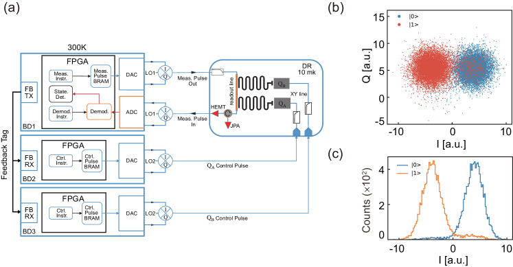
The first FPGA board (BD1) is specially designed for the function of qubit-state readout, called a measure board. With the FPGA algorithm, two digital-to-analog-converters (DACs) output shaped pulses with a carrier frequency smaller than the DAC Nyquist frequency of 500 MHz. They are sent out to an mixer as two quadratures of voltage, and . A microwave source provides a local oscillator (LO) signal ( GHz) for the mixer, which is modulated by the quadratures to generate a readout signal with variable frequency, phase and amplitude KrantzAPR19 . For the detection of returned signal, another mixer mixes down the signal to two quadratures, which are further digitized by two analog-to-digital-converters (ADCs) in BD1. With a demodulation processing (see Appendix C), the readout result is represented as data points in a two-dimensional plane spanned by and .
In our experiment, the readout pulse has a quick initial overshoot and a following sustain part JeffreyPRL14 ; MalletNat09 . The readout pulse is applied for a projective measurement, in which the qubit is projected to the ground or excited state with probabilities determined by the final qubit state before measurement. With a 800 ns long readout pulse and a repetition of the same measurement for many times (), a typical distribution of readout result for QB is shown in the plane in Fig. 1(b). The blue and red dots represent result for the ground and excited state, respectively. They are observed to be two separated humps of data points. The distribution of each hump can be fitted with a Gaussian function, from which a center of the hump can be determined. A line symmetrically intersecting the connection line of two centers can be chosen as a threshold to separate two qubit states. By adjusting the initial phase of the readout pulse, the connection line of two hump centers can be intentionally rotated to be horizontal in the plane. Then the threshold is the voltage of the midpoint between two centers. The threshold value has been shifted to 0 in the shown figure.
The number of data points is integrated with respect to the axis and the histogram of is shown in Fig. 1(c). For the ground state , the main Gaussian hump is on the right side with larger than . For the excited state , the main Gaussian hump is on the left side with smaller than . For both and , there are still scattered data points on the other side of the threshold line. The readout fidelity of the ground (excited) state is defined as the fraction of counted points with larger (smaller) than over , leading to and in Fig. 1c. For the other qubit , the two readout fidelities are and . The readout fidelity for the excited state is normally smaller than that for the ground state, mainly due to the qubit decay error in the measurement process.
The BD1 board enables a multiplexed dispersive readout, in which readout pulses at different frequencies can be multiplexed in the same readout line chenyuAPL12 . The readout signal is finally demodulated to different channels, giving the qubit state result for each individual qubit. In the current version, the FPGA algorithm in BD1 admits a simultaneous measurement of eight qubits.
In the feedback control, a signal qubit is chosen to provide a feedback tag for the superconducting qubit system. By comparing each measured with the threshold value, the qubit state of the signal qubit is determined to be at the ground or excited state. Correspondingly a feedback tag can be generated and transferred from the feedback transmit (TX) to the receive (RX) channels of other FPGA boards (called control board). After receiving a feedback tag, the control boards (BD2 and BD3) can output a conditional shaped pulse. The DAC output is up-converted by the mixer and another microwave source (LO2 with GHz) to the qubit transition frequency. The different feedback-tag-controlled pulses are transferred through control lines to the corresponding qubits to implement a conditional quantum gate. For example, if QA is designated as the signal qubit, the feedback-tag-controlled output of BD2 is a feedback control on QA, and the similar output of BD3 is a feed-forward control on QB. The DAC output of BD2 and BD3 also provide pulses for general qubit operations of QA and QB, respectively. With the integrated multi-boards and ISA (see Appendix D), this scheme can be extended to a superconducting system with many qubits, and multiple signal qubits can be chosen for the feedback control in each subgroup of qubits.
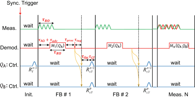
The three boards and the microwave source are phase-locked to an external 10 MHz clock. The timing between different boards are synchronized, with the time dependent pulse sequence shown in the schematic diagram in Fig. 2. The feedback latency in the feedback loop can be correspondingly determined. In all related time scales, is the readout pulse length and is the pulse length of the conditional gate. These two scales are variable parameters in the feedback loop. Starting from the readout pulse, there is a total delay in the low-temperature analog devices and cables, , before the signal returns to the ADC. In Appendix C, we carefully explain other latencies of room-temperature electronics. The latency is introduced by the ADC, which is about ns. The demodulation processing takes a delay of ns, determined by the clock period (4 ns) and number of flip-flops used in the FPGA fabric. The latency is measured to be 24 ns on the oscilloscope. After receiving the feedback tag, there is another delay (68 ns) before the conditional gate pulse is sent out. We define a total delay for the room temperature electronics, , which is 140 ns in the current status. The optimized enables a fast feedback control in our setup.
III Results
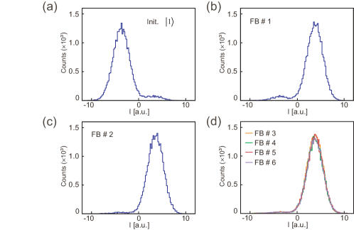
The feedback control is first applied to reset a qubit to the ground state , which can simply prove the realization of a feedback function RistePRL12 . The Xmon qubit QA is utilized for this single-qubit experiment. The idle qubit is initially prepared at the excited state with a calibrated pulse. Afterwards a feedback-reset-gate is applied, which includes a dispersive qubit state measurement and a conditional control pulse. If the qubit is measured to be at the excited state, the conditional control is designated as a pulse to reset the qubit to the ground state. If the qubit is measured to be at the ground state, the control gate is instead designated as an empty sequence but waiting for the same time as the duration of the pulse. Afterwards the qubit is measured again to check the effectiveness of the feedback-reset-gate. The same procedure has been repeated for times. We integrate the number of data points with respect to the axis and show the histograms of in Fig. 3. In Fig. 3(a), the main distribution of data points shows a hump with Gaussian distribution on the left side, with smaller than . The calculated ratio of the excited-state probability is . For the qubit-state measurement after the conditional feedback control, most of the data points in Fig. 3(b) concentrate on the right side, also showing a hump with Gaussian distribution. The main distribution of qubit state shifts from the left side to the right side means that the initialized qubit (at excited state ) is reset to the ground state , by the conditional feedback control. In Fig. 3(b), a small hump can also be observed on the left side with a probability of . Compared to the initialized ground state, this hump is a little bit higher RistePRL12 . The feedback function can be enabled consecutively for multiple times HuNat19 ; AndersenNpjQi19 ; NegnevitskyNat19 . After the 2nd measurement, we apply another conditional gate based on the measurement result. Then a 3rd measurement is taken to check the result, with the histogram of shown in Fig. 3(c). Compared with Fig. 3(b), Fig. 3(c) shows a similar distribution, but with the small hump on the left side depressed to a probability of RistePRL12 . The similar feedback control has been repeated for six times, with the multiple measurements shown in Fig. 3(d). The consecutive feedback controls lead to a steady state. For the result with six feedback loops, the calculated ground state probability is .
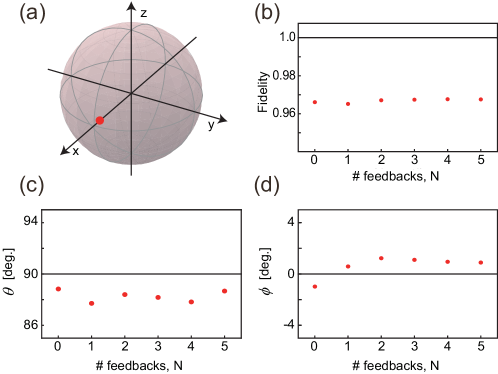
Reset the qubit to the ground state is a special application of the feedback control. Because of the flexibility of the conditional gate, the feedback control can be applied to prepare the qubit to any quantum state on the Bloch sphere CampagnePRX13 . The superposition state is taken as an example. The qubit is initialized at by a rotation around the axis. Then the qubit is measured with a projective measurement. If the qubit is projected to the ground (excited) state, a conditional pulse around the () axis encoded in the algorithm is applied in the feedback control. No matter what the intermediate measurement result is, the qubit is brought back to the state .
A quantum state tomography (QST) is applied to measure the state after the feedback control (see Appendix A) ChuangBook ; SteffenPRL06 . For any qubit state, a density matrix can be expanded as , where and are the identity and pauli matrices. Determined with the QST measurement, the Bloch vector can be depicted as a single point on the Bloch sphere. In this experiment, the same procedure is repeated for times for every QST projection direction. As shown in Fig. 4(a), the Bloch vector of the prepared state is plotted, which points to the axis and is consistent with the expected state of . With the known ideal state, the fidelity of the prepared state is calculated to be . Similar to the reset experiment, the qubit state can be prepared to the designated state by consecutive feedback controls. All the intermediate qubit-state readout is a projective measurement. After a finite times of conditional feedback controls, the final qubit state is measured with a QST. For consecutive states, and of the Bloch vector are displayed in Fig. 4(c) and 4(d), respectively. The error of is all smaller than and the error of is all smaller than . As shown in Fig. 4(b), the fidelity of consecutive state is all larger than .
A feedback control applies a conditional gate to a qubit based on the measurement result of the qubit itself. For a multi-qubit system, a feed-forward control can provide special applications in the quantum information processing RisteNat13 ; SteffenNat13 . To prove the feed-forward function, we choose as a signal qubit, and as a target qubit. The feedback tag is generated based on the projective measurement of the signal qubit. Then a feedback-tag-controlled conditional pulse is issued to the target qubit. The two qubits are physically separated by three qubits in the linear array. To ignore any residue interaction, the signal qubit is biased away from the sweet point, at GHz. The frequency difference between two qubits is increased to MHz, and two qubits are effectively decoupled from each other. At this operation point of , the energy relaxation time is 9.3 s and the pure dephasing time is 1.2 s.
As a simple example, the signal qubit is initialized at . The projective measurement of the signal qubit is applied for the feed-froward control on the target qubit , as shown in the schematic diagram in Fig. 5(a). In this experiment, the same procedure has been repeated for times. For the initialized , there is a larger probability of for the detection of signal larger than 0. Correspondingly the probability of signal smaller than 0 is . For an ideal state of , there should be an equal probability of for the qubit to be projected to the state of and . After a measurement correction (see Appendix B), the corrected populations of are and , close to the ideal equal probabilities. This result suggests that the state preparation and measurement (SPAM) errors contribute to the main error.
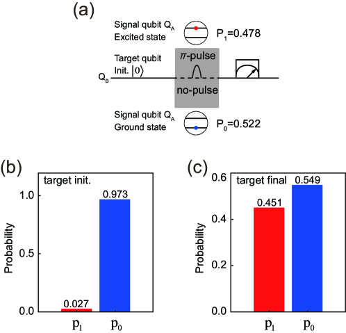
For the target qubit , it is initialized at the ground state , with a measured histogram shown in the bottom left panel in Fig. 5(b). For simplicity, we integrate the number of data points in the plane for both smaller and larger than zero, and show two ratio bars for the ground and excited state probabilities. The probability of larger than is for the initialized target qubit . For the feed-forward control, a (empty) pulse is applied to if is measured to be at the excited (ground) state. Afterwards the qubit state of is measured for checking the function of the feed-forward control. From an ensemble measurement of the target qubit , its state probability is determined as shown in the histogram in Fig. 5(c). With the signal qubit in the state of , there is approximately a probability for the qubit to be pumped to the excited state. With a relative smaller ratio () for to be in the excited state, there is also a relative smaller ratio () for to be pumped to the excited state. The probability for to be at () can be statistically calculated by (), where and are the initialized probabilities of and , respectively. The calculated result is and . After a measurement correction (Appendix A), the calculated result can be calibrated to and , close to the experimental result of and .
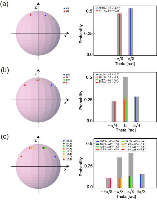
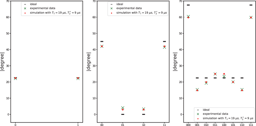
For the random walk experiment, qubit is utilized as a signal qubit and prepared at . The projective measurement of this qubit produces a quantum random number of 0 or 1, and a corresponding feedback tag to control the target qubit. The target qubit is initially prepared at the ground state (the north pole in the Bloch sphere). Depending on the 1st measurement of the signal qubit, the feedback control is a conditional pulse to rotate the target qubit away from the north pole. For the signal qubit measured in the ground or excited state, we rotate around the -axis or -axis with angle , respectively. After the operation of or , a collection of tomography pulses are further applied for the QST measurement of . In the following experiment, the procedure is repeated for times for each QST projection direction. Because we can record each measurement result of the signal qubit, the measurement for the target qubit with and rotations can be separately collected for the QST measurement. For an example of , the tomography result for the one-step random walk is shown in the Bloch sphere in Fig. 6(a). Looking at the -plane from the -axis, the state vector is observed to rotate to the right or left side of the north pole. In the right panel of Fig. 6(a), we show both measured angles of the state vector in the QST. To distinguish the two random-walk directions, the clockwise rotation is labeled with a positive angle while the anticlockwise rotation is labeled with a negative angle. The measured angles slightly deviate from the ideal value with an error of and for signal qubit at and , respectively. The percentage of the collected data in QST is also shown for the two vectors. There is a relative larger ratio () for the target qubit to rotate clockwise, due to the larger ratio for signal qubit at (without correction). The background grey bars are centered at ideal angles, while the height of each grey bar is set to the corresponding experimental result.
To apply consecutive feed-forward controls for the multi-step random walk on the Bloch sphere, the signal qubit is simultaneously frozen at by a feedback control at each step. After the 1st measurement of the signal qubit, the target qubit is rotated clockwise or anticlockwise, with an angle of or . After the 2nd measurement of the signal qubit, the target qubit is assigned to rotate again depending on the feedback tag, no matter how the 1st-step rotation evolves. The target qubit is then appended with tomography pulses for the final-state determination. Here the feedback measurement can be collected to four groups , with the two numbers representing the 1st and 2nd measurement results of the signal qubit. For each group of ensemble measurement, the tomography result is collected for extracting the final state on the Bloch sphere, as shown in Fig. 6(b). If a reversed walk is involved, the qubit is rotated back to be close to the north pole, as shown for the two vectors related with and . In the right panel of Fig. 6(b), we present measured angles of state vectors and corresponding percentages of collected data for the two-step random walk. For signal qubit at state of and , the measured angles deviate from the ideal value with an error of and , respectively. For groups of and , a small difference happens between the percentages of two vectors, due to the slight variation of probabilities for consecutive prepared state of the signal qubit. The height of the central grey bar is set to the addition of two percentages. A three-step random walk is similarly actuated by the simultaneous feedback and feed-forward control, with the results shown in Fig. 6(c). For groups of and , the measured angles deviate from ideal values with an error of and , respectively. Compared with angles related wtih and in the two-step random walk, and angles related with and in the one-step random walk, the angle error increases with the number of walk steps, which is found to be related with the qubit decay and dephasing in the simulation analysis (see Appendix E). For groups of , and , state vectors share similar vector angles around , and the height of the grey bar is set to the addition of three percentages. The similar behavior happens for groups of , and . The measured random walk of target qubit on the Bloch sphere proves both the realization of consecutive feedback/feed-forward control and the precise quantum control in our superconducting multi-qubit system.
IV Summary
We develop a fast FPGA-based feedback control system, with the latency of room-temperature electronics optimized to 140 ns. The function of feedback control is proved by resetting the qubit to the ground state and preparing the qubit to a designated superposition state with high-fidelity. In two-qubit experiments, projective measurement of the signal qubit provides a feed-forward control to the target qubit. The consecutive and simultaneous feedback and feed-forward control enables a random walk of the target qubit on the Bloch sphere. Our experiment is a conceptually simple benchmark for the feedback control, the realization of which proves that the control system is appropriate for a multi-qubit experiment. Furthermore, the hardware and ISA can be expanded to more complex feedback applications, such as the hardware accelerator of error correction code and the compiler of high level quantum language.
Acknowledgements.
The work reported here was supported by the National Key Research and Development Program of China (Grant No. 2019YFA0308602, No. 2016YFA0301700), the National Natural Science Foundation of China (Grants No. 11934010, No. 11775129), the Fundamental Research Funds for the Central Universities in China, and the Anhui Initiative in Quantum Information Technologies (Grant No. AHY080000). Y.Y. acknowledge the funding support from Tencent Corporation. This work was partially conducted at the University of Science and Technology of the China Center for Micro- and Nanoscale Research and Fabrication.Appendix A Quantum State Tomography (QST) Measurement
To fully determine the quantum state of a two-level qubit, we need to realize the quantum state tomography (QST) measurement. The density matrix of either a pure or mixed state can be expanded as , with . We introduce three Pauli operators, , , and , based on which a vector of Pauli operators is represented by . The three projections, , and along the three directions, determine a vector, , which is named as the Bloch vector. The -projection, , is extracted from a projective measurement of the qubit probability. To extract the -projection, we rotate the quantum state by an angle of around the -axis and the density matrix is changed to be , where is an unitary operator for a rotation angle of around the -axis. Experimentally, the gate is realized by a calibrated pulse with the frequency . The rotated density matrix is then given by . The population measurement determines the -projection, , where and are the populations of the ground and excited states in the rotated density matrix. In practice, the gate is also applied for the measurement and the -projection is averaged from the results under the operations of the and gates. The -projection is similarly obtained using the operations of the and gates.
Appendix B Measurement Correction
From the readout fidelity measured for both ground () and excited () state, we could observe that the measured population probabilities () are often different from the ideal result (). The relation between the ideal and measured populations can be expressed as
| (7) |
from which the ideal populations can be calibrated from measured population probabilities.
Appendix C Latency of Electronics
FPGA logic latency. The digital circuit is designed on a Xilinx Kintex-7 (XC7K325T) field-programmable-gate-array (FPGA). We use SystemVerilog language to describe the digital circuit and use the Xilinx Vivado Design Suite to simulate, synthesize and finally implement the design on FPGA XilinxVDS . Data path logic for all the FPGA design runs at 250 MHz clock frequency, leading to a 4 ns latency for each flip-flop. This flip-flop latency is relatively shorter than that of other FPGA chips, such as Xilinx Virtex-4 and Virtex-6 SalathPRAppl18 ; HuNat19 .
We include both signal detection and waveform generation in the multi-board feedback control system. For the measure board, one FPGA chip is integrated with two digital-to-analog-converters (DACs) and two analog-to-digital-converters (ADCs). For the control board, one FPGA chip is integrated with four digital-to-analog-converters (DACs).
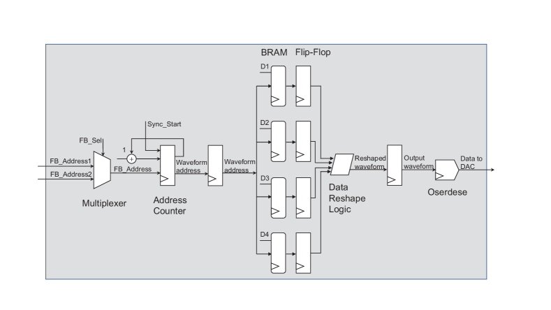
The DAC actuate latency is the time for FPGA to send digital waveform to the DAC card after it receives the trigger signal. A block diagram of the corresponding data path is shown in Fig. 7. The control pulse waveform is stored in Block Random Access Memories (BRAMs) of the FPGA, the read address of which can be determined by a feedback signal. One sample of digital waveform is readout from the BRAM every clock cycle (4 ns) and then streamed to the DAC. We parallelize BRAMs as 4 paths to achieve the total throughput of 1 GSPS, which matches the sampling rate of DAC. Signal delay of the BRAM output is a critical path, thus we insert a flip-flop after the output data of BRAM to pipeline the data path. Because of the similar reason, we insert a flip-flop both after the address counter and after the data reshape logic. With the oserdes XilinxIDDR module introducing one more clock cycle, the total DAC actuate latency is ns.
For the analog-to-digital-converter (ADC) signal processing latency, the block diagram of the data path is shown in Fig. 8. The path is composed of three parts, the ADC input pre-processing, the measure signal demodulation, and the state discrimination. In the first part, two channels of ADC output enter the FPGA. Each ADC has a resolution of 8 bits, working at a conversion rate of 1 GSPS. Correspondingly the ADC presents 2 adjacent digitized samples (16 bits) to the FPGA pad every 2 ns. With the data path clocked every 4 ns, we use Xilinx s input-double-data-rate (IDDR) primitive XilinxIDDR to register the ADC data twice every clock cycle. The DDR module is configured as the SAMEEDGEPIPELINED mode. In this mode, it outputs pairs D1 and D2 to the FPGA logic at the same clock edge, with a delay of 2 clock cycles relative to the input XilinxIDDR . For every clock cycle, D1 is the first 2 ns samples data and D2 the second 2 ns samples data. To simplify the logic design, 2 ns samples are adjacently summed up to a 9-bit data. Here we halve the ADC sampling rate without losing much useful information, because the ADC input signal is within the cutoff frequency of 250 MHz of the ADC anti-aliasing filter. The summed 9-bit data is flip-floped before going to the next stage.
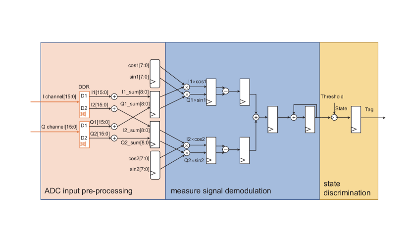
The following stage of demodulation works in several independent and parallel channels. The number of channels that can be implemented is limited by the available FPGA resource, especially the DSP48E1 slice XilinxDSP48E1 . In our current design, we implement eight qubit channels, with each channel discriminating one qubit state and generating one feedback tag. For the signal demodulation, the digital signal is multiplied with a reference signal, summed and accumulated for a window of clock cycles for the final demodulation result. The complex output signal is
| (8) |
in which is the reference frequency. Each is determined by the readout resonator of corresponding qubit. In the demodulation processing, both the real and imaginary part are implemented, with the final result denoted as a single point in the complex plane. The phase information of can be adjusted by introducing an extra phase shift in either the readout pulse or the reference signal. Correspondingly the connection line of the qubit state hump centers can be rotated to be horizontal in the plane. Then the real part of the demodulation result can be used to discriminate the qubit state and generate a feedback tag. For simplicity, the block diagram in Fig. 8 only shows the real part processing. Four flip-flops introduce 4 clock cycles of latency in the demodulation stage. In the third part, the accumulated component is compared to the feedback threshold and a feedback tag is generated, with one extra flip-flop. The total ADC signal processing latency is then ns. Note that the threshold is pre-loaded to the FPGA from the host computer, and eight different thresholds can be set for different qubit channels.
We also apply a waveform record module for timing analysis. The input signal is similarly through the DDR as in the ADC signal demodulation logic. Afterwards the record function is triggered by the synchronous start signal. The ADC input signal is written to the SRAM after 3 clock cycles, with a latency of 12 ns. Using this module, we can experimentally measure the delay of the qubit readout chain. When including the wiring in the DR, the total chain delay is 160 ns. Bypassing the long microwave coax lines in the dilution refrigerator, the total chain delay or the homemade electronics delay is measured to be 96 ns.
Inter board communication latency. In the multi-qubit feedback control system, the measure board generates feedback tags, 1 or 0, based on the discriminated qubit state. In our current design, tags from 8 parallel channels are encapsulated to a packet and transmitted to other control boards (BD2, BD3) through the tag transmission logic. Ethernet cable is used as the physical channel between the measure board and the control board. The cable includes both the forward and receive lines, and tags are sent in the direction from the measure board to the control board. The channel width is thus 2 in one ethernet cable, meaning a two-bit data can be transferred simultaneously. The feedback tag packet is designed as the following format,
| 1 | Qubit1 | Qubit3 | Qubit5 | Qubit7 |
|---|---|---|---|---|
| 1 | Qubit2 | Qubit4 | Qubit6 | Qubit8 |
in which two rows represent parallel lines of the two-bit data. The first column of 2 bits is the head of the tag packet, indicating the beginning of the tag communication. The two-bit head of packet brings one clock cycle before the control board receives the tag. The following bits include tag results of different qubits. If only some of the eight channels are utilized, a default tag value of 1 is set for all unused channels.
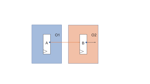
Experimentally, we choose a cable whose length is 1.5 m. With a propagation of 0.6 times the speed of light, the signal delay in the ethernet cable is 8.3 ns. We also estimate a delay of about 8 ns on the PCB trace and the pad to flip-flop delay inside of the FPGA. In the FPGA design, we route the tag output of the measure board (the output of flip-flop A in Fig. 9) to an output pin of the FPGA (labeled O1). We also route the flip-flopped tag input (the output of flip-flop B in Fig. 9) to its FPGA’s output pin (labeled O2). We probe the two signals at O1 and O2 using an oscilloscope to measure the delay of a tag packet, which is around 20 ns and close to the wiring delay plus one flip-flop delay. Including an extra cycle of packet head, the total latency of feedback tag communication is then 24 ns.
Digital/Analog conversion latency. The digital to analog conversion latency is defined as the interval between FPGA sending out the digital waveform data and the DAC daughter card outputting the base-band waveform to the mixer. Similarly, the analog to digital conversion latency is the interval between ADC daughter card receiving the readout waveform and the FPGA receiving the digitized waveform data. Both the DAC and ADC latency are mainly determined by the DAC and ADC chip we selected.
We measure the delay of ns with an oscilloscope. It is the time elapsed from the start trigger of the board to the first point of the signal at the input of its mixer. Three parts contribute to the DAC latency . One is the internal latency of the DAC chip. From the data sheet of AD9736 chip DAC , the analog output changes () clock cycles (1 ns/cycle) after the input data changes, in which the 4 clock cycles is the internal first-in-first-out (FIFO) latency we set. The second is the DAC actuate latency 24 ns, coming from the total pipeline stages of our customized FPGA logic as shown in Fig. 7. The rest latency is ns, which is expected due to the off-chip PCB trace and other small components.
The ADC pipeline delay is the number of clock cycles needed for analog to digital conversion. In the datasheet of ADC081000 chip ADC , this delay is 8 ns if working at the sampling rate of 1 GSPS. There is another 2.7 ns delay for digital data going out of the ADC chip ADC . Experimentally, we actuate a square pulse and trigger the measure board to record it to the BRAM in FPGA, using the waveform record module of the measure board. The timing lag of the recorded square pulse is measured to be 96 ns, which indicates the base-band loop back time. This lag is composed of , measure pulse recording latency (12 ns), the internal latency of the ADC chip, and the off-chip signal delay of the ADC card. We can estimate the off-chip signal delay as ns. The ADC latency is correspondingly estimated to be ns. The total feedback latency of room-temperature electronics is then ns. In the future the latency can be further improved by dealing with different parts, such as choosing DAC/ADC chips with better specifications. We can also choose system-on-chip (SoC) that further integrate hardware components like the FPGA, DAC, ADC, and filter on a single chip.
Appendix D Board Programming Model
Board programming model is also critical in the feedback control system. In Ref. FuMICRO17 , the authors combine the codeword-triggered pulse generation and queue-based event timing control to a centralized quantum control box. Similarly, C. A. Ryan et al. use the super-scalar architecture and dispatch instructions to different working engines RyanRSI17 . In our work we adopt a different strategy and define a measure/control instructions set architecture (ISA) for the deployment of quantum feedback tasks.
This ISA includes multiple instructions executed by multiple boards, and it directly handles the pulse streaming and digital signal processing in measurement. For a new experiment, digital pulse waveforms and all instructions are loaded to each board from the host computer. The host also loads control information to the registers of each FPGA, such as, 8-qubit channels threshold of measure board, the tag select number of control board. Each board starts to execute its instructions after receiving the synchronous trigger signal.
A measure instruction contains the information for the qubit demodulation as below.
| Channel mask[7:0] | Repetition[3:0] | Delay[15:0] | Length[7:0] |
Channel mask is 8 bits and each bit enables a qubit demodulation channel. Repetition is the number of consecutive feedbacks. Delay is the number of cycles delayed before the demodulation (see Fig. 2). Length is the number of cycles of the demodulation window.
A control instruction for one board contains the information to generate the control pulse.
| Opcode[3:0] | Index0[7:0] | Index1[7:0] | Address0[19:0] | Address1[19:0] |
Opcode directs the type of instructions. If , the board will terminate the execution of the instruction. If , when the current item is completed, the board will execute the next instruction. If , when the current item is completed, the board will jump to the instruction at index0. If , when the current item is completed, the board will jump to the instruction conditioned on the received feedback tag. The tag for the next instruction must be valid before the current instruction finishes. Index0 and index1 are the address of next instruction, conditioned on the tag. Address0 and address1 determine the segment of waveform in the BRAM, with the digital waveform sequence starts from address0 and ends at address1.
This ISA is reduced to basic functions of reading the pulse waveform and demodulation reference from the main memory, which brings flexibilities and several advantages. First, because the timing scheduling is set by the host computer, we can interleave instructions for fine-grained gate timing optimization in feedback. In contrast, the centralized superscalar architecture suffers great timing cost in the feedback trigger synchronization (210 ns) and address jumping (53 ns) RyanRSI17 . Second, with the pulse waveform and measure reference pre-loaded to each board, we can reuse the memory by only loading new gates for the next task, which greatly reduces the host-board communication. Third, runtime variables can be set on the fly by the host computer. This feature can be very useful when adaptively calibrating the multi-qubit system, e.g., the adjust of feedback threshold. In general, the ISA naturally supports the feedback/feed-forward control with multiple signal qubit and multiple target qubit. On the other hand, this ISA mimics features of a traditional computer model, like memory operation, branching, MIMD (multiple instruction, multiple data), therefore it is promising to integrate the ISA with classical processors. In the future, more complex functions can be built upon this ISA, such as the compiler of quantum feedback program, hardware accelerator of the error correction code and quantum feedback runtime.
Appendix E Simulation of the random walk result
We numerically simulate the target qubit’s random walk result, using the master equation,
| (9) |
in which are coupling terms through which the system couples to the environment. are the Lindblad operators and are the corresponding rates. For Xmon-type qubits, system-environment coupling is related with two independent channels, characterized by the relaxation term and pure dephasing term , with and , respectively.
When we simulate the random walk with infinite and , the rotation angle of the target qubit is almost the same as the ideal values. When parameters are set as S and S, the simulation result reproduces a deviation of rotation angle of the target qubit away from ideal values (not shown), with the same tendency as that in the experimental data. However, a remaining difference exists between the experimental and simulation result. Here we mention a technical detail in the experimental process. During the random walk process of the target qubit, the measurement of signal qubit is found to induce an ac-Stark shift of the target qubit LiuPRX16 ; AndersenNpjQi19 ; SchusterPRL05 , represented by a small detuning of MHz (or 15 degree phase shift per step). A square-shaped -pulse is applied to the target qubit to compensate this phase offset before the next step. We suspect that the signal qubit’s readout pulse may account for a larger pure dephasing rate of the target qubit. After adjusting the parameter , we found the simulation with S and S is well consistent with the experimental data, as shown in Fig. 10. This simulation result indicates that the qubit decay and dephasing induce the deviation of the roation angle away from ideal values.
References
- (1) M. A. Nielsen and I. Chuang, Quantum Computation and Quantum Information, Cambridge University Press, Cambridge, England, 2010.
- (2) M. Sarovar, H. S. Goan, T. P. Spiller, and G. J. Milburn, High-Fidelity Measurement and Quantum Feedback Control in Circuit QED, Phys. Rev. A. 72, 062327 (2005).
- (3) N. Yamamoto, Coherent Versus Measurement Feedback: Linear Systems Theory for Quantum Information, Phys. Rev. X 4, 041029 (2014).
- (4) P. Krantz, M. Kjaergaard, F. Yan, T. P. Orlando, S. Gustavsson, and W. D. Oliver, A Quantum Engineer’s Guide to Superconducting Qubits, Appl. Phys. Rev. 6, 021318 (2019).
- (5) K. Geerlings, Z. Leghtas, I. M. Pop, S. Shankar, L. Frunzio, R. J. Schoelkopf, M. Mirrahimi, and M. H. Devoret, Demonstrating a Driven Reset Protocol for a Superconducting Qubit, Phys. Rev. Lett. 110, 120501 (2013).
- (6) S. Shankar, M. Hatridge, Z. Leghtas, K. M. Sliwa, A. Narla, U. Vool, S. M. Girvin, L. Frunzio, M. Mirrahimi, and M. H. Devoret, Autonomously Stabilized Entanglement between Two Superconducting Quantum Bits, Nature 504, 419 (2013).
- (7) J. Kelly, R. Barends, A. G. Fowler, A. Megrant, E. Jeffrey, T. C. White, D. Sank, J. Y. Mutus, B. Campbell, Y. Chen, Z. Chen, B. Chiaro, A. Dunsworth, I. C. Hoi, C. Neill, P. J. J. O’Malley, C. Quintana, P. Roushan, A. Vainsencher, J. Wenner, A. N. Cleland, and J. M. Martinis, State Preservation by Repetitive Error Detection in a Superconducting Quantum Circuit, Nature 519, 66 (2015).
- (8) Y. Liu, S. Shankar, N. Ofek, M. Hatridge, A. Narla, K. M. Sliwa, L. Frunzio, R. J. Schoelkopf, and M. H. Devoret, Comparing and Combining Measurement-Based and Driven-Dissipative Entanglement Stabilization, Phys. Rev. X 6, 011022 (2016).
- (9) C. K. Andersen, A. Remm, S. Lazar, S. Krinner, N. Lacroix, G. J. Norris, M. Gabureac, C. Eichler, and A. Wallraff, Repeated Quantum Error Detection in a Surface Code Christian, arXiv:1912.09410 (2019).
- (10) R. Vijay, C. Macklin, D. H. Slichter, S. J. Weber, K. W. Murch, R. Naik, A. N. Korotkov, and I. Siddiqi, Stabilizing Rabi Oscillations in a Superconducting Qubit Using Quantum Feedback, Nature 490, 77 (2012).
- (11) D. Risté, C. C. Bultink, K. W. Lehnert, and L. Dicarlo, Feedback Control of a Solid-State Qubit Using High-Fidelity Projective Measurement, Phys. Rev. Lett. 109, 240502 (2012).
- (12) D. Risté, M. Dukalski, C. A. Watson, G. De Lange, M. J. Tiggelman, Y. M. Blanter, K. W. Lehnert, R. N. Schouten, and L. Dicarlo, Deterministic Entanglement of Superconducting Qubits by Parity Measurement and Feedback, Nature 502, 350 (2013).
- (13) L. Steffen, Y. Salathe, M. Oppliger, P. Kurpiers, M. Baur, C. Lang, C. Eichler, G. Puebla-Hellmann, A. Fedorov, and A. Wallraff, Deterministic Quantum Teleportation with Feed-Forward in a Solid State System, Nature 500, 319 (2013).
- (14) P. Campagne-Ibarcq, E. Flurin, N. Roch, D. Darson, P. Morfin, M. Mirrahimi, M. H. Devoret, F. Mallet, and B. Huard, Persistent Control of a Superconducting Qubit by Stroboscopic Measurement Feedback, Phys. Rev. X 3, 021008 (2013).
- (15) G. de Lange, D. Risté, M. J. Tiggelman, C. Eichler, L. Tornberg, G. Johansson, A. Wallraff, R. N. Schouten, and L. Dicarlo, Reversing Quantum Trajectories with Analog Feedback, Phys. Rev. Lett. 112, 080501 (2014).
- (16) N. Ofek, A. Petrenko, R. Heeres, P. Reinhold, Z. Leghtas, B. Vlastakis, Y. Liu, L. Frunzio, S. M. Girvin, L. Jiang, M. Mirrahimi, M. H. Devoret, and R. J. Schoelkopf, Extending the Lifetime of a Quantum Bit with Error Correction in Superconducting Circuits, Nature 536, 441 (2016).
- (17) C. A. Ryan, B. R. Johnson, D. Rist , B. Donovan, and T. A. Ohki, Hardware for Dynamic Quantum Computing, Rev. Sci. Instrum. 88, 104703 (2017).
- (18) Y. Masuyama, K. Funo, Y. Murashita, A. Noguchi, S. Kono, Y. Tabuchi, R. Yamazaki, M. Ueda, and Y. Nakamura, Information-to-Work Conversion by Maxwell’s Demon in a Superconducting Circuit Quantum Electrodynamical System, Nat. Commun. 9, 4 (2018).
- (19) Y. Salathé, P. Kurpiers, T. Karg, C. Lang, C. K. Andersen, A. Akin, S. Krinner, C. Eichler, and A. Wallraff, Low-Latency Digital Signal Processing for Feedback and Feedforward in Quantum Computing and Communication, Phys. Rev. Appl. 9, 034011 (2018).
- (20) L. Hu, Y. Ma, W. Cai, X. Mu, Y. Xu, W. Wang, Y. Wu, H. Wang, Y. P. Song, C. L. Zou, S. M. Girvin, L. M. Duan, and L. Sun, Quantum Error Correction and Universal Gate Set Operation on a Binomial Bosonic Logical Qubit, Nat. Phys. 15, 503 (2019).
- (21) C. K. Andersen, A. Remm, S. Lazar, S. Krinner, J. Heinsoo, J. C. Besse, M. Gabureac, A. Wallraff, and C. Eichler, Entanglement Stabilization Using Ancilla-Based Parity Detection and Real-Time Feedback in Superconducting Circuits, Npj Quantum Inf. 5, 69 (2019).
- (22) R. Barends, J. Kelly, A. Megrant, A. Veitia, D. Sank, E. Jeffrey, T. C. White, J. Mutus, A. G. Fowler, B. Campbell, Y. Chen, Z. Chen, B. Chiaro, A. Dunsworth, C. Neill, P. J. J. O’Malley, P. Roushan, A. Vainsencher, J. Wenner, A. N. Korotkov, A. N. Cleland, and J. M. Martinis, Superconducting Quantum Circuits at the Surface Code Threshold for Fault Tolerance, Nature 508, 500 (2014).
- (23) X. Fu, M. A. Rol, C. C. Bultink, J. Van Someren, N. Khammassi, I. Ashraf, R. F. L. Vermeulen, J. C. De Sterke, W. J. Vlothuizen, R. N. Schouten, C. G. Almudver, L. DiCarlo, and K. Bertels, An Experimental Microarchitecture for a Superconducting Quantum Processor, Proc. 50th Annu. IEEE/ACM Int. Symp. Microarchitecture - MICRO-50 17 813 (2017).
- (24) J. M. Gambetta, J. M. Chow, and M. Steffen, Building Logical Qubits in a Superconducting Quantum Computing System, Npj Quantum Inf. 3, 2 (2017).
- (25) F. Arute, K. Arya, R. Babbush, D. Bacon, J. C. Bardin, R. Barends et al., Quantum supremacy using a programmable superconducting processor, Nature 574, 505 (2019).
- (26) Yu Chen, D. Sank, P. O’Malley, T. White, R. Barends, B. Chiaro, J. Kelly, E. Lucero, M. Mariantoni, A. Megrant, C. Neill, A. Vainsencher, J. Wenner, Y. Yin, A. N. Cleland, John M. Martinis, Multiplexed Dispersive Readout of Superconducting Phase Qubits, Appl. Phys. Lett. 101, 182601 (2012).
- (27) M. D. Reed, B. R. Johnson, A. A. Houck, L. Dicarlo, J. M. Chow, D. I. Schuster, L. Frunzio, and R. J. Schoelkopf, Fast Reset and Suppressing Spontaneous Emission of a Superconducting Qubit, Appl. Phys. Lett. 96, 203110 (2010).
- (28) E. Jeffrey, D. Sank, J. Y. Mutus, T. C. White, J. Kelly, R. Barends, Y. Chen, Z. Chen, B. Chiaro, A. Dunsworth, A. Megrant, P. J. J. O’Malley, C. Neill, P. Roushan, A. Vainsencher, J. Wenner, A. N. Cleland, and J. M. Martinis, Fast Accurate State Measurement with Superconducting Qubits, Phys. Rev. Lett. 112, 190504 (2014).
- (29) R. Barends, J. Kelly, A. Megrant, D. Sank, E. Jeffrey, Y. Chen, Y. Yin, B. Chiaro, J. Mutus, C. Neill, P. O. Malley, P. Roushan, J. Wenner, T. C. White, A. N. Cleland, and J. M. Martinis, Coherent Josephson Qubit Suitable for Scalable Quantum Integrated Circuits, Phys. Rev. Lett. 111, 080502 (2013).
- (30) A. Dunsworth, A. Megrant, C. Quintana, Zijun Chen, R. Barends, B. Burkett, B. Foxen, Yu Chen, B. Chiaro, A. Fowler, R. Graff, E. Jeffrey, J. Kelly, E. Lucero, J. Y. Mutus, M. Neeley, C. Neill, P. Roushan, D. Sank, A. Vainsencher, J. Wenner, T. C. White, and John M. Martinis, Characterization and Reduction of Capacitive Loss Induced by Sub-micron Josephson Junction Fabrication in Superconducting Qubits, Appl. Phys. Lett. 111, 022601 (2017).
- (31) Z. Zhang, T. Wang, L. Xiang, Z. Jia, P. Duan, W. Cai, Z. Zhan, Z. Zong, J. Wu, L. Sun, Y. Yin and G. Guo, Experimental Demonstration of Work Fluctuations along a Shortcut to Adiabaticity with a Superconducting Xmon Qubit, New J. Phys. 20, 085001 (2018).
- (32) T. Wang, Z. Zhang, L. Xiang, Z. Jia, P. Duan, W. Cai, Z. Gong, Z. Zong, M. Wu, J. Wu, L. Sun, Y. Yin, and G. Guo, The Experimental Realization of High-Fidelity Shortcut-to-Adiabaticity Quantum Gates in a Superconducting Xmon Qubit, New J. Phys. 20, 065003 (2018).
- (33) T. Wang, Z. Zhang, L. Xiang, Z. Jia, P. Duan, Z. Zong, Z. Sun, Z. Dong, J. Wu, Y. Yin, and G. Guo, Experimental Realization of a Fast Controlled-Z Gate via a Shortcut to Adiabaticity, Phys. Rev. Appl. 11, 034030 (2019).
- (34) J. Koch, T. M. Yu, J. Gambetta, A. A. Houck, D. I. Schuster, J. Majer, A. Blais, M. H. Devoret, S. M. Girvin, and R. J. Schoelkopf, Charge-Insensitive Qubit Design Derived From the Cooper Pair Box, Phys. Rev. A. 76, 042319 (2007).
- (35) T. Roy, S. Kundu, M. Chand, A. M. Vadiraj, A. Ranadive, N. Nehra, M. P. Patankar, J. Aumentado, A. A. Clerk, and R. Vijay, Broadband Parametric Amplification with Impedance Engineering: Beyond the Gain-Bandwidth Product, Appl. Phys. Lett. 107, 262601 (2015).
- (36) F. Mallet, F. R. Ong, A. Palacios-Laloy, F. Nguyen, P. Bertet, D. Vion, and D. Esteve, Single-Shot Qubit Readout in Circuit Quantum Electrodynamics, Nat. Phys. 5, 791 (2009).
- (37) V. Negnevitsky, M. Marinelli, K. K. Mehta, H. Y. Lo, C. Fl hmann, and J. P. Home, Repeated Multi-Qubit Readout and Feedback with a Mixed-Species Trapped-Ion Register, Nature 563, 527 (2018).
- (38) M. Steffen, M. Ansmann, R. Mcdermott, N. Katz, R. C. Bialczak, E. Lucero, M. Neeley, E. M. Weig, A. N. Cleland, and J. M. Martinis, State Tomography of Capacitively Shunted Phase Qubits with High Fidelity, Phys. Rev. Lett. 97, 050502 (2006).
- (39) Xilinx Inc., Vivado Design Suite User Guide UG892 (v2018.2), https://www.xilinx.com/support/documentation/swmanuals/xilinx20182/ug892-vivado-design-flows-overview.pdf (June 6, 2018).
- (40) Xilinx Inc., 7 Series FPGAs SelectIO Resources: User Guide, Ug471, (v1.10 May 8, 2018).
- (41) Xilinx Inc., 7 Series DSP48E1 Slice: User Guide, Ug479, (v1.10 March 27, 2018).
- (42) Analog Devices, “10-/12-/14-Bit, 1200 MSPS DACS”, AD9734/AD9735/AD9736 datasheet, 2005, [Rev. B].
- (43) Texas Instruments, “ADC081000 High Performance, Low Power 8-Bit, 1 GSPS A/D Converter”, ADC081000 datasheet, Feb. 2004, [Revised Sept. 2013].
- (44) D. I. Schuster, A. Wallraff, A. Blais, L. Frunzio, R. S. Huang, J. Majer, S. M. Girvin, and R. J. Schoelkopf, ac Stark Shift and Dephasing of a Superconducting Qubit Strongly Coupled to a Cavity Field, Phys. Rev. Lett. 94, 123602 (2005).