Extraordinary high room-temperature carrier mobility
in graphene-WSe2 heterostructures
High carrier mobilities play a fundamental role for high-frequency electronics (?), integrated optoelectronics (?) as well as for sensor and spintronic applications (?, ?), where device performance is directly linked to the magnitude of the carrier mobility. Van der Waals heterostructures (?) formed by graphene and hexagonal boron nitride (hBN) already outperform all known materials in terms of room temperature mobility (?). Here, we show that the mobility of today’s best graphene/hBN devices can be surpassed by more than a factor of three by heterostructures formed by tungsten diselenide (WSe2), graphene and hBN, which can have mobilities as high as 350,000 cm2/(Vs) at room temperature, and resistivities as low as Ohm. The resistivity of these devices shows a much weaker temperature dependence than the one of graphene on any other known substrate. The origin of this behaviour points to modified acoustic phonon bands in graphene and questions our understanding of electron-phonon scattering in van der Waals heterostructures.
Stacking two-dimensional materials into van der Waals heterostructures allows engineering their electronic, magnetic and optical properties (?). For example, the interaction between graphene and hBN can modify graphene’s electronic band structure, (?, ?) while twisting individual sheets in bilayer graphene can result in a Mott-like insulating state (?) or in superconductivity (?). Stacking different materials can also give rise to significant changes in the phonon dispersion relation (?, ?, ?, ?). However, modifications of the phonon band structure have mostly been neglected in graphene-based heterostructures so far , because of the good agreement between electronic transport measurements and theoretical predictions based on electron-phonon scattering in pristine graphene (Gr). Here we show that this is not true for WSe2/Gr/hBN heterostructures, which show room-temperature mobilities well above the upper limit predicted by theory for pristine graphene (?, ?).
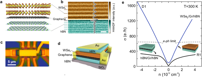
The devices were fabricated using a 30 to 50 nm-thick WSe2-crystal to delaminate graphene grown by chemical vapor deposition (CVD) from its copper substrate, and to deposit it on a pre-exfoliated hBN-flake on silicon dioxide on a highly-dopped silicon substrate (?, ?), which acts as a back gate (see Methods). Cross-sectional scanning transmission electron microscopy (STEM) measurements reveal clean interfaces between both hBN/Gr and Gr/WSe2, as indicated in Fig. 1b. The layer spacing between graphene and the first WSe2 layer is Å (see Supplementary Methods), in good agreement with ab-initio calculations but substantially smaller (by 1.5 Å) than previously reported for bulk WSe2 on hBN (?).
The heterostructures were shaped into Hall bars with one-dimensional Cr/Au side contacts. For comparison, we also fabricated CVD-graphene devices with identical geometries but based on regular hBN/Gr/hBN stacks (?). One of the WSe2/Gr/hBN devices (device D1) features also an additional metallic top gate (see Fig. 1c,d), allowing to independently control the carrier density in WSe2 and graphene, respectively. Accurate measurements on this device indicate that WSe2 does not significantly contribute to the conductivity away from graphene’s charge neutrality point, providing only a weak parallel conduction channel not tuned by the back-gate. We estimate the electrostatic coupling to the back-gate and the charge carrier density in graphene using both Hall and quantum Hall measurements (see Supplementary Methods).
The room-temperature longitudinal conductivity of two representative devices is shown in Fig. 1e as a function of graphene’s charge-carrier density . The conductivity of the reference hBN/Gr/hBN-sample (R1) exhibits the typical behaviour of state-of-the-art high-mobility graphene devices, i.e. it saturates at conductivity values of a few hundred at large carrier densities, which is a hallmark of increasing electron-phonon scattering (?, ?). By contrast, the conductivity of the WSe2/Gr/hBN-device D1 shows an almost linear behavior over the full electron () and hole () regime, reaching values more than four times higher than those of the reference sample, and corresponding to resistivity values as low as 15 Ohm.
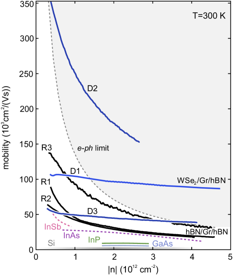
We estimate the mobility of the devices, , by fitting the conductivity data with the linear relation , where is the residual conductivity at the charge neutrality point (see Methods). The room-temperature mobility of three different WSe2/Gr/hBN devices (D1-D3) is plotted in Fig. 2, together with the one of three reference samples based on hBN/Gr/hBN (R1-R3). Among these, R1 and R2 have the same Hall-bar geometry as D1-D3, while the data labeled as R3 corresponds to those originally published in Ref. (?), which are among the highest mobility values reported so far. At high carrier density (cm-2), all reference devices show a room-temperature mobility of a few 104cm2/(Vs), in agreement with theoretical predictions for phonon-limited conductivity in intrinsic graphene (?, ?, ?). This behavior has to be contrasted with the one of the devices based on WSe2/Gr/hBN. Device D1 (shown also in Fig. 1) has an almost constant room-temperature mobility of 100,000 cm2/(Vs). A second device (D2) shows even larger mobility, reaching 350,000 cm2/(Vs) at low carrier densities, and remaining well above 150,000 cm2/(Vs) for cm-2, well beyond what is currently understood as the upper limit to the room-temperature mobility of graphene devices (gray dashed-line in Fig. 2). The third device based on WSe2/Gr/hBN (D3) shows a more standard performance, with room-temperature mobility below 100,000 cm2/(Vs). This device appears, however, to be strongly limited by impurity scattering, as reflected by a low temperature mobility of only 50,000 cm2/(Vs) (see Supplementary Fig. S7b).
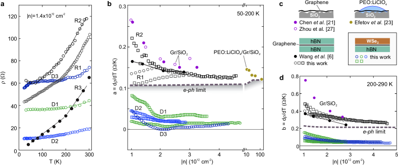
To investigate the origin of the high room-temperature mobility of the WSe2/Gr/hBN devices, we study the resistivity as a function of temperature at constant carrier density, as presented in Fig. 3a for cm-2. For all values of , the resistivity of the devices based on WSe2/Gr/hBN presents a remarkably weaker increase with temperature than the one of the reference devices. We use a linear fit to extract the slope of the resistivity in the temperature regime K (the so-called “equipartition regime”), where the resistivity is expected to grow linearly with temperature (?). The results are presented in Fig. 3b, where we also compare with data from literature for graphene on SiO2 with (?) and without electrolyte gating (?, ?). At low densities (cm-2), there is a relatively large scattering of data points and a clear dependence on , which can be accounted to temperature-broadening effects as well as to the stronger influence of impurity scattering and electron-electron interaction at low carrier density. Vice versa, for cm-2 the slope of the resistivity becomes essentially density-independent, and data points from different samples cluster around two well-distinct limit values: one close to zero for WSe2/Gr/hBN devices, and a larger one for all other devices.
A similar trend is also observed at higher temperatures, between K. Using a linear fit to extract the slope of the resistivity also in this temperature range, we find that the values of extracted from WSe2/Gr/hBN devices are consistently smaller than the ones extracted from the reference samples, with the latter ones coming close to the value predicted by theory at high density (see Fig. 3c). The suppression of in WSe2/Gr/hBN devices is proportionally stronger than the one of (see Supplementary Fig. S13), indicating that a single scaling factor cannot account for the weaker temperature dependence of the resistivity of these devices with respect to the reference samples.
This behaviour challenges our current understanding of the resistiviy of graphene devices. For the sake of clarity, we focus our discussion on the equipartition regime ( K) at high carrier density (cm-2). Today it is widely accepted that in this regime the minimal resistivity of graphene is due to scattering with in-plane acoustic phonons mediated by gauge-field coupling, with only minor contributions from displacement-field coupling (?, ?, ?). Scattering with optical phonons (either intrinsic or from the substrate) is expected to be strongly suppressed, while other sample-dependent mechanisms, such as impurity scattering or umklapp electron-electron scattering (?), if present, act as additional scattering channels and increase the total resistivity. The linear increase of the resistivity with temperature can then be described in terms of a proportionality factor, , which depends only on the dispersion relation of the acoustic phonons, , where is the effective sound velocity, and on the dimensionless gauge-field parameter (see Supplementary Discussion).
The gauge-field parameter is essentially an intrinsic property of graphene. In a tight-binding framework, it is directly connected to the derivative of the nearest-neighbor hopping integral with respect to the carbon-carbon bond length (?). This parameter can be accurately estimated by ab-initio calculations (?), it is doping-independent, unaffected by screening, and robust with respect to changes in the Fermi velocity due to unscreened electron-electron interactions at low carrier density. Considering gauge-field as the only source of scattering leads to a systematic underestimation of the resisitivity of graphene, however, it is sufficient to increase the ab-initio value of by 15 % to obtain good agreement between theory and experimental data for graphene on SiO2, with and without electrolyte gating (?). The same holds true for graphene encapsulated in hBN, as reflected also in Fig. 3b. Only the WSe2/Gr/hBN devices are significant outliers with respect to the theoretical prediction. The small values of observed in the WSe2/Gr/hBN devices would call for a reduction of by a factor with respect to the theoretical estimate (and by a factor 2.7 with respect to the fitted value), which is very hard to explain.
Other possibilities to account for the suppression of in WSe2/Gr/hBN devices are modifications of the electronic or of the phononic bands. Significant modifications of the electronic band structure can be excluded, at least above cm-2, because the quantum Hall measurements performed on our samples (see Supplementary Fig. S5) indicate a linear dispersion relation. As long as the dispersion relation is linear, modifications of the Fermi velocity have no net effect on and on the resistivity. Modifications of the phonon dispersion relation appear then as the most plausible cause of the suppressed resistivity of the WSe2/Gr/hBN devices.
These could be due to, e.g., strain in the graphene sheet, which modifies the acoustic sound velocity . However, fitting the data of Fig. 3b requires more than a doubling of in WSe2/Gr/hBN devices, and this cannot be explained by the weak compressive strain (below 1 %) indicated by Raman spectroscopy measurements in these devices (see Supplementary Fig. S8c). On the other hand, Raman spectroscopy measurements on suspended WSe2/Gr samples reveal the existence of an additional Raman-active phonon mode at cm-1 (5.5 meV), characteristic of the WSe2/Gr interface (see Supplementary Fig. S9). This mode could be the signature of an inter-layer shear mode between graphene and WSe2. The presence of a shear mode would cause the opening of a finite energy gap in the dispersion relation of the in-plane acoustic modes , which in turn would lead to a strong suppression of the resistivity of the system. Indeed, modifying the model of Ref. (?) to account for such a square-root phonon-dispersion relation and taking as a fit-parameter, we find good quantitative agreement with our experimental results, with values of ranging from 50 cm-1 to 180 cm-1 (622 meV; see Supplementary Discussion).
Conjecturing the existence of a shear-mode at the graphene-WSe2 interface allows for a simple and physically appealing explanation of our data. However, the origin of the required mechanical inter-layer coupling at the microscopic level remains unclear. Ab-initio calculations predict values of that are far too weak to explain our results (see Supplementary Discussion). However, to the best of our knowledge, there are no other physical mechanisms that could account for the behaviour of our devices, at least within the framework of our current understanding of the resistivity of graphene-based heterostructures. The extraordinary-high room-temperature mobilities of our WSe2/Gr/hBN devices are a clear example of the fact that, despite more than a decade of intensive research, graphene still hold secrets.
Acknowledgements: The authors thank V. Falko, A. Geim and L. Wirtz for helpful discussions. This work was supported by the European Union’s Horizon 2020 Research and Innovation Program under grant agreement No 785219 (Graphene Flagship), the Deutsche Forschungsgemeinschaft (DFG, German Research Foundation) under Germany’s Excellence Strategy - Cluster of Excellence Matter and Light for Quantum Computing (ML4Q) EXC 2004/1 - 390534769 (Gefördert durch die Deutsche Forschungsgemeinschaft im Rahmen der Exzellenzstrategie des Bundes und der Länder - Exzellenzcluster Materie und Licht für Quanteninformation (ML4Q) EXC 2004/1 - 390534769), by DFG through BE 2441/9-1, and by the Helmholtz-Nano-Facility (HNF) (?). Growth of hexagonal boron nitride crystals was supported by the Elemental Strategy Initiative conducted by the MEXT, Japan, A3 Foresight by JSPS and the CREST(Grant No. JPMJCR15F3), JST. Computing resources were provided by PRACE on Marconi at CINECA, Italy (Project ID 2016163963).
Author contributions: L.B., B.B. and C.S. conceived the experiment. L.B. fabricated the devices. L.B. and A.E. performed the measurements. L.B., T.S. and C.S. analysed the data. T.S., N.M., F.L., F.M. carried out the theoretical analysis. L.B., T.S., F.H., B.B. and C.S. wrote the manuscript with input from all authors. K.B. and T.T. provided hBN flakes. Electron microscopy and data analysis was performed by F.W. and K.MC.
Competing interests: The authors declare no competing financial interests.
Methods: Device fabrication – The van der Waals heterostructures studied in this work are assembled using a dry transfer technique based on CVD-grown graphene crystals and exfoliated crystals of hexagonal boron nitride (hBN) and tungsten diselenide WSe2 (?, ?). Graphene (Gr) is picked-up directly from the copper growth-substrate using a WSe2-flake (supplier: HQ graphene), and deposited on a pre-exfoliated hBN-flake on a Si++/SiO2 substrate, where the heavily doped Si++ is used as a back gate. The heterostructures are then shaped into Hall-bars following the method of Wang et al. (?), using SF6/Ar-based reactive ion etching and evaporating Cr/Au one-dimensional contacts. For one device (device D1, shown in Fig. 1a), after this first metallization step, we transferred a second hBN flake on top of the device, on which we evaporate a Cr/Au top-gate. Finally, a TEM lamella was prepared exactly from the chip region using focused ion beams, and investigated by STEM.
Transport measurements – Transport measurements were carried out using standard lock-in techniques ( Hz), using a 4-terminal measurement configuration: A small AC voltage is applied between the source and drain contacts of the Hall bars and and are measured parallel and perpendicular to the current direction, respectively. All transport data shown in the main manuscript are carried out in a variable temperature insert (VTI) ranging from 2K to 300K. Mobility values are extracted by fitting conductivity measurements with the formula in the range – cm-2, where is the charge-carrier density in graphene. The extracted values for the residual conductivity of devices D1–D3 and R1, R2 are: e2/h, e2/h, e2/h, e2/h and e2/h. In all measurements presented in the manuscript and in the supplementary material (except for those of Fig. S1 and Fig. S2a-b), the voltage on the top gate of D1 was set to .
Data and materials availability: All relevant data are available from the corresponding author upon request.
Supplementary Information: Supplementary information accompanies this paper.
References
- 1. Lin, Y.-M. et al. 100-GHz Transistors from Wafer-Scale Epitaxial Graphene. Science 327, 662 (2010).
- 2. Bonaccorso, F., Sun, Z., Hasan, T. & Ferrari, A. C. Graphene photonics and optoelectronics. Nat. Photonics 4, 611–622 (2010).
- 3. Dauber, J. et al. Ultra-sensitive Hall sensors based on graphene encapsulated in hexagonal boron nitride. Appl. Phys. Lett. 106, 193501 (2015).
- 4. Han, W., Kawakami, R. K., Gmitra, M. & Fabian, J. Graphene spintronics. Nat. Nanotechnol. 9, 794–807 (2014).
- 5. Geim, A. K. & Grigorieva, I. V. Van der Waals heterostructures. Nature 499, 419–425 (2013).
- 6. Wang, L. et al. One-Dimensional Electrical Contact to a Two-Dimensional Material. Science 342, 614–617 (2013).
- 7. Dean, C. R. et al. Hofstadter’s butterfly and the fractal quantum Hall effect in moiré superlattices. Nature 497, 598–602 (2013).
- 8. Hunt, B. et al. Massive Dirac Fermions and Hofstadter Butterfly in a van der Waals Heterostructure. Science 340, 1427–1430 (2013).
- 9. Cao, Y. et al. Correlated insulator behaviour at half-filling in magic-angle graphene superlattices. Nature 556, 80–84 (2018).
- 10. Cao, Y. et al. Unconventional superconductivity in magic-angle graphene superlattices. Nature 556, 43–50 (2018).
- 11. Balandin, A. A. Phonon engineering in graphene and van der Waals materials. MRS Bull. 39, 817–823 (2014).
- 12. Lui, C. H. et al. Observation of interlayer phonon modes in van der Waals heterostructures. Phys. Rev. B 91, 165403 (2015).
- 13. Narang, P., Zhao, L., Claybrook, S. & Sundararaman, R. Effects of Interlayer Coupling on Hot-Carrier Dynamics in Graphene-Derived van der Waals Heterostructures. Adv. Opt. Mater. 5, 1600914 (2017).
- 14. Greener, J. D. G. et al. Coherent acoustic phonons in van der Waals nanolayers and heterostructures. Phys. Rev. B 98, 075408 (2018).
- 15. Hwang, E. H. & Das Sarma, S. Acoustic phonon scattering limited carrier mobility in two-dimensional extrinsic graphene. Phys. Rev. B 77, 115449 (2008).
- 16. Sohier, T. et al. Phonon-limited resistivity of graphene by first-principles calculations: Electron-phonon interactions, strain-induced gauge field, and Boltzmann equation. Phys. Rev. B 90, 125414 (2014).
- 17. Banszerus, L. et al. Ultrahigh-mobility graphene devices from chemical vapor deposition on reusable copper. Sci. Adv. 1, e1500222 (2015).
- 18. Banszerus, L. et al. Identifying suitable substrates for high-quality graphene-based heterostructures. 2D Mater. 4, 025030 (2017).
- 19. Rooney, Aidan. P. et al. Observing Imperfection in Atomic Interfaces for van der Waals Heterostructures. Nano Lett. 17, 5222–5228 (2017).
- 20. Dean, C. R. et al. Boron nitride substrates for high-quality graphene electronics. Nat. Nanotechnol. 5, 722–726 (2010).
- 21. Chen, J.-H., Jang, C., Xiao, S., Ishigami, M. & Fuhrer, M. S. Intrinsic and extrinsic performance limits of graphene devices on SiO2. Nat. Nanotechnol. 3, 206–209 (2008).
- 22. Zou, K., Hong, X., Keefer, D. & Zhu, J. Deposition of High-Quality on Graphene and the Effect of Remote Oxide Phonon Scattering. Phys. Rev. Lett. 105, 126601 (2010).
- 23. Efetov, D. K. & Kim, P. Controlling Electron-Phonon Interactions in Graphene at Ultrahigh Carrier Densities. Phys. Rev. Lett. 105, 256805 (2010).
- 24. Pietronero, L., Strässler, S., Zeller, H. R. & Rice, M. J. Electrical conductivity of a graphite layer. Phys. Rev. B 22, 904–910 (1980).
- 25. Perebeinos, V. & Avouris, P. Inelastic scattering and current saturation in graphene. Phys. Rev. B 81, 195442 (2010).
- 26. Park, C.-H. et al. Electron–Phonon Interactions and the Intrinsic Electrical Resistivity of Graphene. Nano Lett. 14, 1113–1119 (2014).
- 27. Zhao, Y. et al. Interlayer Breathing and Shear Modes in Few-Trilayer MoS2 and WSe2. Nano Lett. 13, 1007–1015 (2013).
- 28. Wallbank, J. R. et al. Excess resistivity in graphene superlattices caused by umklapp electron–electron scattering. Nat. Phys. 15, 32–36 (2018).
- 29. HNF - Helmholtz Nano Facility. Research Center Juelich GmbH, HNF - Helmholtz Nano Facility, Journal of Large-Scale Research Facilities 3, 112 (2017).