Emergent magnetic texture in driven twisted bilayer graphene
Abstract
The transport properties of a twisted bilayer graphene barrier are investigated for various twist angles. Remarkably, for small twist angles around the magic angle , the local currents around the AA-stacked regions are strongly enhanced compared to the injected electron rate. Furthermore, the total and counterflow (magnetic) current patterns show high correlations in these regions, given rise to well-defined magnetic moments that form a magnetic Moiré superlattice. The orientation and magnitude of these magnetic moments changes as function of the gate voltage and possible implications for emergent spin-liquid behaviour are discussed.
Despite its chemical simplicity, twisted bilayer grapheneLopes07 ; Suarez10 ; Bistritzer11 ; Moon12 ; PhysRevLett.108.216802 ; PhysRevB.93.035452 (TBG) hosts a number of surprising phenomena ranging from superconductivity,Cao18b ; Yankowitz19 ; Moriyama19 ; Codecido19 ; Shen19 ; Lu19 correlated insulator phase,Cao18a ; Choi19 emergence of a Hofstadter butterfly,Dean13 ; Kim17 anomalous Hall ferromagnetism,Sharpe19 ; bultinck2019 ; ZhangMao19 photonic crystal for nano-light,Sunku18 and intrinsic optical dichroism.Kim16 ; Zhang18 ; Zhang19 ; bultinck2019 There are also several new predictions such as chiral superconductivity,Lin19 ; Classen19 nematic phases,Kozii18 flat plasmonic bands,Stauber16 a longitudinal Hall effectStauber18 ; Stauber18b , long-lived plasmonsLevitov19 , Moiré ordered current loops,Weckbecker19 and marginal Fermi liquid.Gonzalez19 ; Gonzalez19b The tuneable twist angle thus changes the optical, plasmonic and electronic properties that may be used in novel twisttronic devices.Carr17 There are also related carbon systems such as twisted double-bilayer grapheneLiu19 ; Cao19b ; Shen19 or ABC-trilayer graphene on a -substrateChen19 that show superconducting phases.
The plethora of new phenomena is closely linked to the emergence of a new intermediate length scale given by the Moiré-lattice constant of 10 nm. This superstructure is due to the different crystallographic orientations of the two graphene layers and its periodicity can be defined by quasi-circular AA-stacked regions where the two graphene layers lie on top of each other. These islands are arranged in a triangular lattice, surrounded by AB- and BA-stacked graphene which are the dual configurations of Bernal-stacked bilayer graphene. At small twist angles and low energies, the wave-functions become quasi-localisedTrambly10 ; Trambly12 within the AA-stacked regions, also leading to quasi-localised neutral collective modes.Stauber16
The appearance of an intermediate Moiré scale should also influence the coherent transport properties, especially for filling factors around the charge neutrality point as it gives rise to the aforementioned flat-band physics. In this regime, a paramagnetic orbital response to an in-plane magnetic field is expected that becomes maximal around the magic angle .Stauber18 ; Stauber18b This response is caused by the so-called counterflowBistritzer11 ; Liu17 where the current densities of the two layers move in opposite directions.Bistritzer11
In order to invoke this response electrically, an asymmetric driving with respect to the layers is required. Therefore, we shall here investigate the coherent transport properties of TBG by injecting electrons only in one of the layers. Our main result is the emergence of an AA-enhanced counterflow pattern, interpreted as a periodic magnetic texture due to the orbital motion of the electrons whose magnitude can be tuned by the external source-drain voltage and whose triangular geometry might lead to frustration and spin-liquid behaviour.
I Model
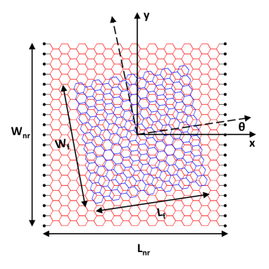
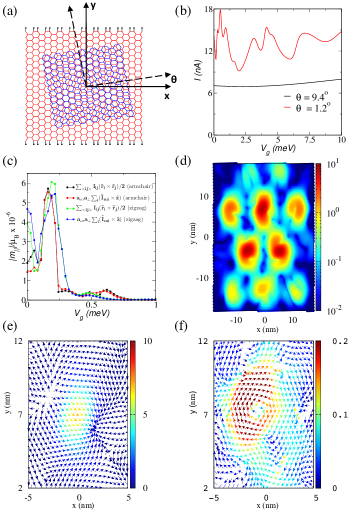
In order to investigate electronic transport through a TBG region with a large magnetic (or counterflow) response, we consider the system sketched in Fig. 1. It consists of a monolayer armchair graphene nanoribbon of width and length with a graphene flake of size on top. When the armchair edges of the nanoribbon and the patch are aligned we have an AB-stacked bilayer graphene region. Changing the orientation of the flake, a TBG barrier is created for the electrons flowing in the nanoribbon. We choose the following dimensions: nm, nm, nm and nm. This setup allows us to reduce the effect of corners, edges and evanescent states that would make the interpretation of the transport mechanisms more challenging. There are 97468 atoms in the bottom layer and 59432 atoms in the top flake. The number of atoms connected to the source and drain contacts amounts to 237.
Although in our setup we can impose any twist angle, we will work with commensurate rotation angles to facilitate notation and comparison to the continuum model.Lopes07 The conductance is calculated within the Landauer-Büttiker formalism , where is the Green’s function of the central region and , are the the self energies of the left and right contact, respectively; in the same way, and define the coupling functions of the central region to the left and right contact.
To describe the low energetic electronic properties, we use a tight-binding Hamiltonian (above denoted as ) with hopping amplitude between sites and , where is the bond length and is the angle formed by and the z-axis. The value of the inter-atomic matrix elements is a function of the bond length:Brihuega12 ; Moon12 where , , , and .
To properly characterize the electronic properties of TBG, one needs to go beyond the nearest-neigbour description, thus for a site we select the neighbours located inside a radius . The previous restriction reduces the efficiency of recursive techniques to calculate the Green’s functions of the central region and the contacts. To overcome these technical problems, we first represent the Hamiltonian of the entire device as a sparse matrix and secondly, we set the self-energy terms to .Bahamon The last approximation is valid whenever a large number of modes is injected into the central region.Schomerus
II Conductance
There are three electronic regimes in TBG.Lopes07 ; PhysRevB.93.035452 For large rotation angles , the layers are basically decoupled at low energies. For intermediate angles with , the two layers become coupled leading to a renormalisation of the Fermi velocity and the emergence of van Hove singularities inside the first Moiré band.Luican11 For small angles , the layers are strongly coupled and low-energetic wave-functions become localized.Trambly10 ; Trambly12
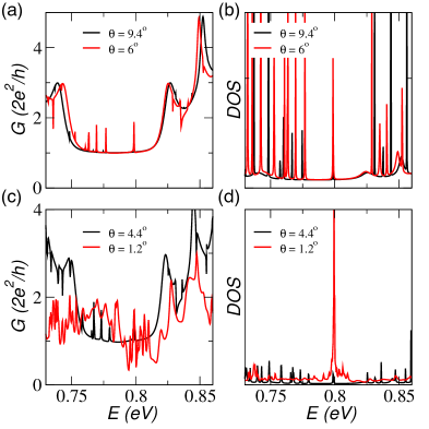
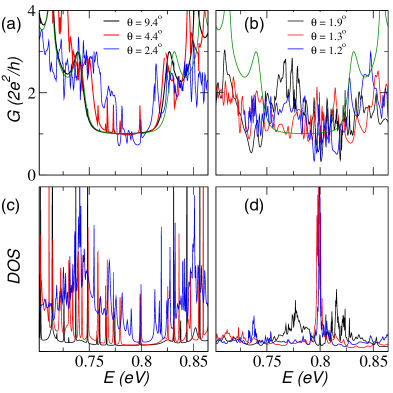
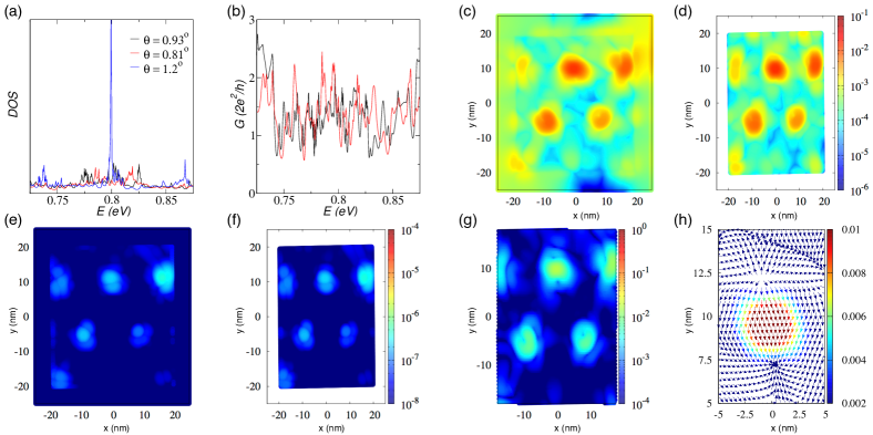
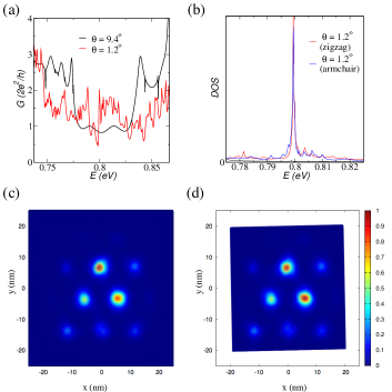
We can observe these regimes also in the conductance of our system where we are especially interested in the transport properties around the charge neutrality point (CNP). Due to self-doping effects, the chemical potential of the CNP is no longer at zero energy, however, we can find it gradually increasing the strength of the TBG barrier. For large angles , the TBG barrier is completely transparent and the conductance of the single layer nanoribbon is not modified by the twisted patch on top. Reducing the twisting angle, in the intermediate coupling regime for , we see in Fig. 2 resonant peaks superimposed on the first conductance plateau as well as the reduction of the width of the plateau. Interestingly, the conductance and DOS peak at appears for all twisting angles and allow us to pinpoint the CNP. To understand this, note that the contacts always inject electrons with a defined momentum , while at the CNP the TBG has only one transmission state with . This momentum mismatchchico produces a quasilocalized state (see ESI†) and introduces an additional channel for transport at the CNP.
In the strong coupling regime (i=27), the conductance quantization is completely gone and rapid oscillations around the CNP appear. In general, frequency as well as intensity of these oscillations become stronger as the twist angle is reduced. The physical origin behind these oscillations is the high Density of States (DOS) around the CNP, see Fig. 2 (d), i.e., the TBG barrier scatters the incident electrons into a large number of available states with the same energy, causing the observed interferences.
We also studied electronic transport for (see ESI†), however, we do not observe high DOS around the CNP. For theses systems the Moiré periodicity Lopes07 , and there are few A-A stacked regions in our device to produce high DOS.
III Local current patterns.
It is important to note that one atom in the bilayer region can have more than 50 neighbors, thus the expression for the current between sites and
| (1) |
where is the lesser Green’s function.Datta , must be used cautiously to calculate the total current at one atomic site. Running backwards from the magnetic moment definition based on bond currents, we provide a consistent definition of the total site current that, by construction, leads to the same magnetic moment.
The classical image of a current-carrying straight wire from to and the classical definition of magnetic moment, , leads to the global definition of magnetic moment Walz :
| (2) |
where means sum over pairs (bonds), counted once. The expression of Eq. (2) can be manipulated as follows:
| (3) |
where we have used that , , , and , where now (and ) runs over all sites. This leads to the following definition of site currents
| (4) |
and the associated expression for the magnetic moment
| (5) |
By construction, both expressions for the magnetic moment give the same answer, of course provided that local currents are associated to both sites of each bond. Notice that, if one just wanted the same magnetic moment, the carbon-carbon distance nm could be any number, provided it is the same object in Eq. (4) and Eq. (5). The choice of a length for is thus arbitrary and included for dimensional homogeneity of and . Eq. (5) can be interpreted as the discrete version of the textbook formula, , at least for a regular array of sites.
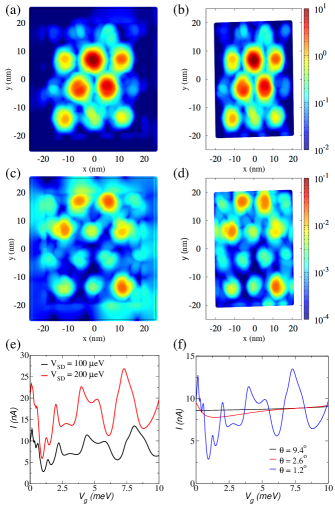
We will now investigate the local current distribution through the TBG sample paez ; Wakabayashi:2001yg ; Liu:2004zr using eq. (4). Since, we are interested in the transport properties around the CNP when high DOS is present, we select the twist angle . To make contact with experiment,Cao18b we fix the bias voltage and study the current distribution as a function of the gate voltage measured from the charge neutrality point (). In Fig. 3, the magnitude of the current on both layers is plotted for , see panels (a) and (b), and for , see panels (c) and (d). The current is normalised by the average bond current injected into the drain contact . For , the total source-drain current is divided by the number of atoms connected to the drain contact, i.e., .
It is clearly seen that there is a strong enhancement of the current in the AA-stacked regions which can be up to twenty times stronger compared to for . The formation of these hot spots can be linked to the enhanced density of states around the CNP observed on the AA-stacked regions. It can also be observed in the continuum model, see ESI†. Even more remarkable is the fact that the current intensity presents similar patterns and values on both layers given the fact that the electrons are injected only into the bottom layer.
To examine the origin of the current in the top layer, we calculated the source-drain current for large and small angles setting . The result is shown in Fig. 3(f). For , the current is carried by one transverse mode in the bottom layer ( where nA/meV). Around the CNP for , the source-drain current is slightly modified, however, when the current map is plotted we observe similar magnitudes in the top and bottom layer and hot spots on the AA-stacked regions (see ESI†). Given that the total source-drain current is not reduced, we are forced to assume that the observed flow of charge is a response of the top layer to the injected current.
IV Chiral response and in-plane magnetic moment
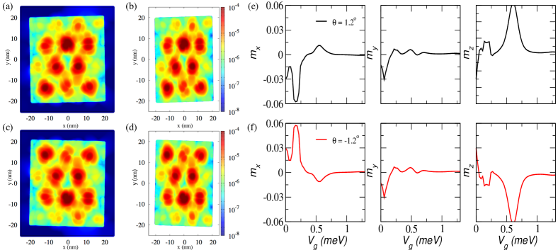
In order to develop a general analysis of the current response of the top layer, we highlight that an applied electric field induces an in-plane magnetic moment in chiral systems. To check if the size our device allows for a magnetic analysis we calculated current, DOS, LDOS and magnetic moment for . The infinite twisted bilayer system can be transformed from a positive to a negative twist angle by performing a parity-transformation and subsequent mirror-transformation ( rotation around the -axis). The position vector, current density, and magnetic moment transform accordingly, i.e., , , and . We observe that LDOS, total magnetic moment and current in our finite system fulfill these requirements for all energy points. Detailed results can be inspected in the ESI†.
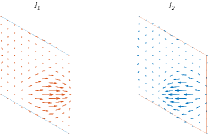
For eV and in Fig. 4(a) and (d), the current is shown in the bottom layer () with a red vector and the current on the top patch () by a blue vector for two mirror-symmetric AA-stacked regions. The current pattern presents a complex structure, the number of neighbours considered in the tight-binding Hamiltonian and the interference effects introduce additional texture in the local current distribution. Despite of these circumstances, there exists a dominant current flow in all AA-stacked regions that produces an orbital magnetic moment. For this, we define the magnetic (or counterflow) and the total current:
| (6) |
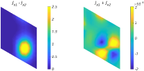
The magnetic current is well aligned and follows the transformation rules presented above, see Fig. 4 (b) for and in Fig. 4 (e) for . Note that the defined pattern of the magnetic current means that the current in both layers flows in opposite directions producing an in-plane magnetic moment. Although the magnitude of total current is about times smaller than the magnetic one, in Fig. 4 (c) and (f) shows a circulating pattern.
Having shown the simplicity of the magnetic current to describe the current response of the AA-stacked regions, let us now discuss the current response of the driven TBG sample in magnetic language. We can define the in-plane magnetic moment in two ways, i.e., globally and locally. The first definition can be written in terms of the bond current as stated by eq. (2) for the whole device. The second definition involves the local magnetic current in the AA-stacked regions and reads
| (7) |
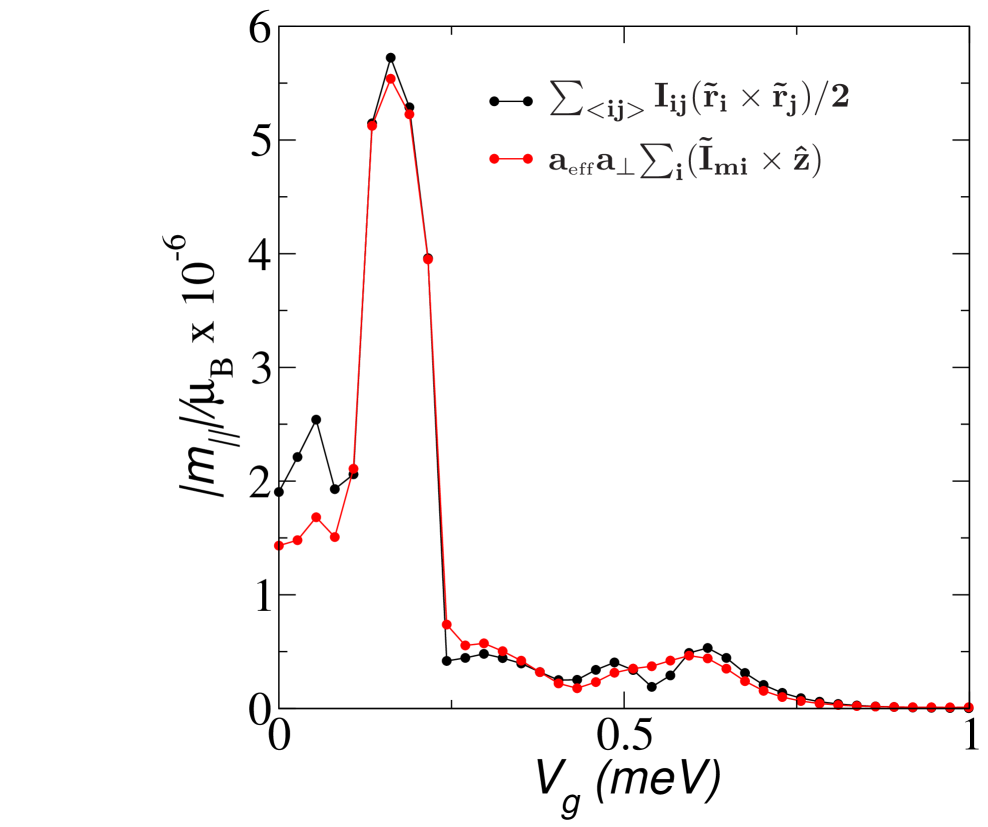
where is the interlayer distance and the out-of-plane unit vector. We also introduced an effective bond length . Its value can be estimated projecting the bond length onto the vectors of the hexagonal lattice . For a nearly prefect match between both approaches we set (see Fig. 5).
In Fig. 5 we calculate the in-plane magnetic moment for the AA-stacked region between and as function of the gate voltage. Clearly both approaches yield very similar results for the in-plane magnetic moment per site in units of Bohr magneton . Although we present the results for one region, other AA-stacked regions present similar behaviour. This is, non-zero in-plane magnetic moment around the CNP and oscillations.
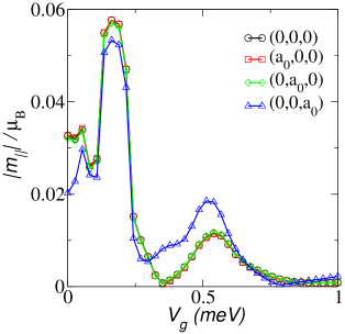
It is important to mention that the expressions for the global and local magnetic moment are only well-defined if the total current vanishes, i.e., in a closed system.PhysRevB.51.11584 This is not the case in our driven system as a net current flows through it, and any change of origin would lead to an additional contribution to the magnetic moment: , with . To find out under what circumstances the magnetic moment is well-defined, we shift the center of our infinite device (TBG barrier + contacts) to positions , and where nm and compare with the original system centred at . It is noticed in Fig. 6 that the in-plane magnetic moment ( and ) is well defined for low gate voltages. This is nicely illustrated for shifts constrained to the xy-plane, where the perfect agreement is a consequence of . The differences observed for out-of-plane displacement can be traced back to a small, but non-zero .
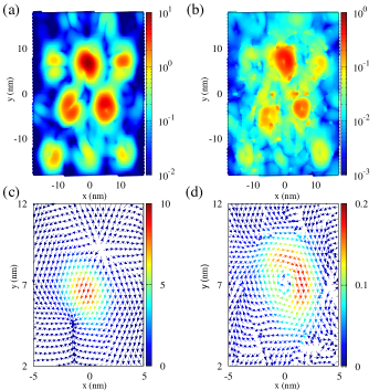
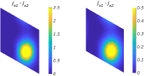
Still, the magnetic moment as obtained from the first definition is almost independent of the choice of the origin. This remarkable result can be understood by looking at the current map of the magnetic and total current whose absolute values differ by two orders of magnitudes, see Fig. 7 (a) and (b). This is particularly clear in the AA-stacked regions: zooming in on one of these regions, a strongly enhanced and highly oriented counterflow is appreciated, see Fig. 7 (c). Therefore, a well-defined local magnetic moment can be attached to each AA-patch, because . The presence of well-localised counterflow patterns must be accompanied by a source and drain. This can be seen from the vectorial map of the counterflow that clearly shows the presence of a source and a sink of the magnetic current on the AA-stacked region. The non-zero divergence of the magnetic current leads to a accumulation of charge on the two layers with opposite sign provoking a current in -direction and thus closing the loop current. Or, to put it in another words, the total out-of-plane current as previously anticipated from the current response of the top layer and the shift of the origin. Let us also note that the direction of the angular magnetic moment of the several patches is not inferred by the source-drain direction, but that it is virtually random and tuneable by the gate-voltage within our finite sample.
It is worth noticing that large orbital magnetic moments also apears in molecular bridgesPhysRevLett.87.126801 and carbon nanotubes,PhysRevB.75.153406 however, its appearance highly depends on the source and drain electrodes. This is not so in our case since our electrodes are not directly attached to the TBG barrier, in fact, they are far form the barrier by approx. 5 nm. Furthermore, linear response within the continuum model for bottom layer driven (infinite) TBG yields the same picture for the in-plane magnetic moment, i.e., large magnetic and small total currents in the AA-stacked regions. This is true for the whole band (not only around the neutrality point) and it also confirms the peculiar nature of the excitations,Stauber18 ; Stauber18b i.e., the current on the bottom layer is opposite to the applied source-drain voltage, see ESI†.
IV.1 Out-of-plane magnetic moment.
The general (global) definition also yields a finite magnetic moment in -direction. This is consistent with a local interpretation since even though is much smaller than , it is finite and shows a vortex structure on the scale of the AA-stacked region as seen in Fig. 7 (d). Moreover, at the atomic level we observe microscopic loop currents around the hexagonal plaquettes of single-layer graphene, giving rise to additional out-of-plane moments, see Fig. 4(c) and (f). Still, this effect seems not as robust as the counterflow.
V Robustness under perturbations
We will now analyze our results in the presence of various perturbations such as lattice relaxation, edge orientation, or edge disorder due to vacancies. It will turn out that the basic features such as the emergence of a magnetic texture are unchanged and should thus be experimentally observable.
V.1 Lattice relaxation
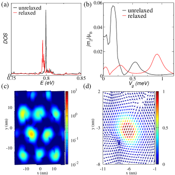
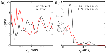
The calculations presented so far assume that the individual graphene layers preserve their crystallographic structure when stacked on top of each other. However, differences among the binding energies of the AA and AB/BA stacked regions lead to lattice relaxation, and this process reduces the area of the AA stacked region. Thus, to address the robustness of the observed magnetic response we follow the procedure presented by Nam and Koshino to include in-plane lattice relaxation.Nam17 ; NamErratum Although the CNP is downshifted to eV, the relaxed lattice continues to present a high DOS around the CNP as represented by the red line in Fig. 8 (a). Importantly, all previously obtained features, i.e., high LDOS, high current and localized magnetic moments on the AA-stacked regions, are robust against lattice relaxation. However, if we compare the LDOS or the current for specific unrelaxed-relaxed lattice regions at the same and , we observe differences with respect to the actual numbers and local distributions. Thus, we cannot expect that the calculated magnetic moments for unrelaxed/relaxed regions present similar lineshapes as function of, e.g., the gate voltage, see Fig. 8 (b). Nevertheless, also in the relaxed lattice we find the emergence of a well defined magnetic texture as shown in Fig. 8 (c)-(d).
Note that our results should thus be a general feature because the most important ingredient to produce the magnetic texture is the wave function localization at the AA-stacked regions, and this effect is robust against in-planeNam17 ; NamErratum and out-plane lattice relaxation.PhysRevB.99.195419 ; Gargiulo_2017 ; Jain_2016
V.2 Zigzag edges
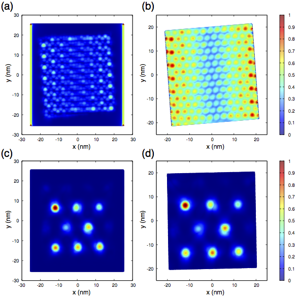
With the aim of simplifying the initial analysis, we selected an armchair nanoribbon as the bottom monolayer of our device. However, it is well known that armchair and zigzag graphene nanoribbon present different electronic transport features. One of these properties is the spatial profile of the current that can have a significant impact on our result, e.g., for low energies, the current in armchair graphene nanoribbons spreads uniformly over the width, while it is highly peaked at the center of the zigzag graphene nanoribbons. Zarbo2007
Now that we have a clear picture of the physical processes occurring within the TBG barrier under the asymmetric driving, we can focus on the response of the TBG barrier embedded in a zigzag graphene nanoribbon (see Fig. 9 (a)). In Fig. 9 (b)-(f), we observe that there is not a qualitative difference between the response of the TBG barrier on top of an armchair or zigzag graphene nanoribbons, i.e., we continue to observe a strong enhancement of the current around the CNP and for low angles and strong in-plane magnetic moments on the AA-stacked regions.
Let us analyse our results in more detail. First, it is worth mentioning that the magnitude of the in-plane magnetic moment for the AA-stacked region between and presents similar values to those of the armchair case as shown in Fig. 9 (c). Second, the magnetic current of the underlying zigzag nanoribbon is rotated by compared to armchair case, shown in Fig. 9(e) and Fig. 7(c), respectively. However, the total current preserves its vortex structure, plotted in Fig. 9(f).
V.3 Edge disorder
Let us finally address the robustness of the in-plane magnetic moments against edge disorder due to vacancies. Although we find a general reduction of the total magnetic moment in the presence of 10% of vacancies in the the top flake edges, our main conclusions still remain unaltered. Details on the calculations can be found in the ESI.
VI Conclusions.
We find a non-trivial texture of angular orbital momentum which is necessarily arranged in a triangular lattice. This is highly reminiscent of a Skyrmion lattice where the spin-texture is defined by circular domain walls which are arranged in a lattice configuration and recently seen in single layer graphene.zhou2019skyrmion We speculate that similar physics might arise in our system. Here, the magnetic texture is highly tuneable since the induced magnetic moments are directly related to the source-drain voltage and can thus be changed from the quantum regime with small magnetic moments to a ”more classical” regime with larger magnetic moments. More importantly, the magnetic moments in the AA-stacked regions are not polarized relative to the direction of the source-drain current and incommensurable twist angles should enhance this effect. The expected dipolar coupling between two localised magnetic moments might thus become important and eventually even lead to collective magnetic behaviour or even to a genuinely two-dimensional spin-liquid state.Han12 This should be measurable in transport or local probe experiments.
The dipolar interactions can directly be tuned by the twist angle which changes the lattice constant of the triangular Moiré-lattice, i.e., for they would differ by a factor of assuming constant localised magnetic moments adjustable by the source-drain voltage. We also envision the possibility of electrical control of magnetic excitations, a long-sought goal in the quest of improved heat management for current technologies based on charged carriers.chumak2015magnon Our setup might further be interesting in view of nano magnetism, usually concerned with using chiral and topological excitations such as skyrmions to store information in small volumes. Here, it would be the size of a Moiré unit cell.
In summary, we presented a transport study of a monolayer armchair and zigzag ribbons with a twisted graphene flake on top. Around the neutrality point, the TBG barrier scatters electrons mainly into evanescent modes and for twist angles around the magic angle, the response is dominated by the large number of localized states on the AA-stacked regions. The high local DOS also gives rise to an enhanced localized counterflow when a source-drain voltage is applied to only one layer, resulting in a highly tuneable lattice of well-defined in-plane orbital magnetic moments with potential technological interest.
In our finite sample, a high local DOS is only seen around the neutrality point, but we expect similar features to be observed for larger filling factors in macroscopic samples where the band-structure has fully developed. This is based on calculations made for the continuum model where the enhanced counterflow exists over the entire first conduction and valence band, respectively.
Acknowledgements
We acknowledge interesting discussions with Nuno Peres. This work has been supported by Spain’s MINECO under Grant No. FIS2017-82260-P, PGC2018-096955-B-C42, and CEX2018-000805-M as well as by the CSIC Research Platform on Quantum Technologies PTI-001. DAB acknowledges financial support from FAPESP (process nos. 2015/11779-4 and 2018/07276-5), CAPES PrInt project no. 88887.310281/2018-00, CNPq process 306434/2018-0 and Mackpesquisa.
Supplementary Information
Conductance, momentum mismatch and charge neutrality point
This section contains a detailed discussion of the conductance and Density of States (DOS) observed in the twisted bilayer graphene (TBG) barrier. In Fig. 10 (a), the conductance for the TBG barrier is shown for intermediate twist angles. The strength of the TBG barrier for is still very weak and the conductance lineshape is similar to the conductance for twist angles (green line in Fig. 10a). For , there are resonant peaks superimposed on the first conductance plateau. There is also a reduction on the width of the same plateau. For the first conductance plateau is strongly reduced.
Irrespective of the rotation angle, there are two key attributes in the conductance of the TBG barrier in this twist angle regime: (i) the reduction of the twist angle introduces a continuous set of conducting states, since there are energy regions with conductance values higher than the ones obtained for the weak coupling regime. In those regions, interference is seen which is a consequence of having more than one conducting channel.gonzalez (ii) There is a conductance peak at .
The physical origin of both attributes can be deduced from the DOS, shown in Fig. 10 (c). The first conductance feature can be understood by noticing that new conducting states rise around when the twist angle is reduced. On the other hand, the transmission peak at signals the position of the charge neutrality point (CNP) of the TBG barrier. This can be understood by noticing that the highly doped left contact injects electrons with a defined momentum which are scattered into a number of available states with momentum , where is the gate voltageTworzydlo06 and the energy at the CNP. At the CNP, the mismatch between the available momenta in the contacts () and the TBG barrier () produces an evanescent state and partial reflection at the barrier. The constructive interference between these waves produces a transmission peak.chico
Notice that the momentum mismatch and hardly depend on the twist angle and the peaks in the conductance and DOS observed for all twist angles at eV indicate the position of . The appearance of the high DOS peak at the same energy in the small angle regime confirms that our transport analysis is correct.
In the small angle regime (), the conductance quantization is completely gone. We can see in Fig. 10 (b) that the conductance shows rapid oscillations around and the frequency as well as the intensity of these oscillations increase as the angle is reduced. The TBG barrier thus again scatters incident electrons into different channels with the same energy. However, in the small angle regime there is a higher DOS around , shown in Fig. 10 (d). Consequently, the electrons transmit through a larger number of propagating states generating more complex interference patterns.
Local Density of States
In Fig. 11 (a) and (b), we have plotted the local Density of States (LDOS) for the for the state at and twist angle . The state presents all the characteristics of an evanescent state: high LDOS at the edges that decays towards the center of the TBG barrier. However, the top and bottom layer are still weakly coupled since the LDOS is not evenly distributed over both layers. Consequently, in this regime the top patch behaves as an additional channel for the transport.
In the small angle regime, the interference discussed above is also appreciated looking at LDOS. In Fig. 11 (c) and (d), the LDOS is shown for at . The high LDOS is unevenly distributed over the AA-stacked regions as a result of the multiple electronic paths. The lower LDOS in the regions close to the edges of the top graphene flake are finite size effects indicating a reduction of the Moiré confinement potential. In the small angle regime, electrons thus transmit through the sample via a number of degenerate states localized on AA-stacked regions.
Charge neutrality of bulk TBG
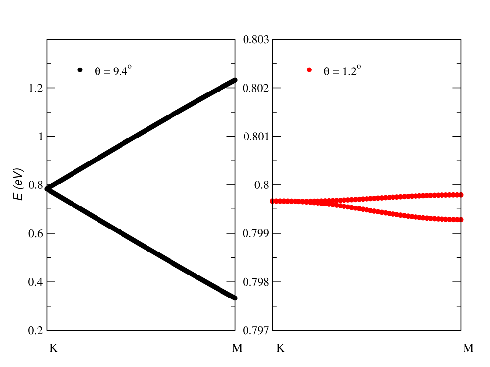
For an additional confirmation of the CNP location, we calculated the band structure for bulk TBG for different twist angles. The CNP of the bulk system is located around the same value we obtained from transport calculations of our finite system, see Fig. 12.
Based on the above and the conductance calculation, we can confirm that our finite system reproduces the main features reported for bulk TBG for . Although DOS plots of our device show oscillations due to the confinement, we clearly observe: (i) new vHs with the reduction of the twist angle, (ii) Merging of vHs for small angles and (iii) localization of the wave function on AA-stacked regions.
Twist angles beyond the magic angle
For , there is no high DOS at the charge neutrality point as shown in Fig. 13 (a). Still, there is a high LDOS on the AA-stacked regions. For small twist angles, the Moiré periodicity almost exceeds the dimension of the top layer and the few AA-stacked regions are not enough to produce a DOS peak at the CNP. From the transport point of view, the TBG efficiently scatters electrons into the available states producing interference as seen from the rapid oscillations in the conductance, see Fig. 13 (b).
Regarding the main results presented in the main text, we continue observing high current density and in-plane magnetic moments on the AA-stacked regions since these effects are the result of having high LDOS on those regions. To assert the above mentioned, we plot for a TBG barrier with , and the magnitude of the electric current divided by the source-drain current per bond in Fig. 13(c)-(d) and the in-plane magnetic moment in panels (e)-(f) calculated by the global formula . The maps allow us to identify that in spite of the low number of AA-stacked regions the injected current still produces charge current and in-plane magnetic moments “hot spots”. Moreover, because of the greater Moiré periodicity the in-plane magnetic moments appear totally localized on the central AA-stacked regions. The current counterflow maps (Fig. 13(g)-(h)) also show high values and preferred orientation on the same regions.
Local definition of the magnetic moment and chiral response
To check if the system size allows for a general analysis, we perform the calculations for a positive and negative twist angle. The infinite twisted bilayer system can be transformed from a positive to a negative twist angle by performing a parity-transformation and subsequent mirror-transformation ( rotation around the -axis). The position vector, current density, and magnetic moment transform accordingly, i.e., , , and .
In Fig. 14, we can see that our finite system fullfil these requirements. Looking first at the map of in-plane magnetic moment ( and ) in panels (a)-(d), a large magnetic moment is seen at the AA-stacked regions. These regions transforms as and can be linked to the high LDOS and current densities , present on the same spots. To underline the transformation of the magnetic moment, we plot the components in units of as function os in panels (e)-(f). Let us also mention that the sign change of under the transformation points at the chiral coupling of TBG as discussed in Ref. 28.
Defining the in-plane magnetic moment
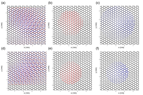
The calculation of the magnetic and total current at the atomic sites is only well-defined in the AA-stacked regions where the atoms have approximately the same x and y coordinates. At these sites, and are well defined. To extend the calculation to other regions of the device, it is necessary to average the current on both layers. Our process is divided in two steps.
-
•
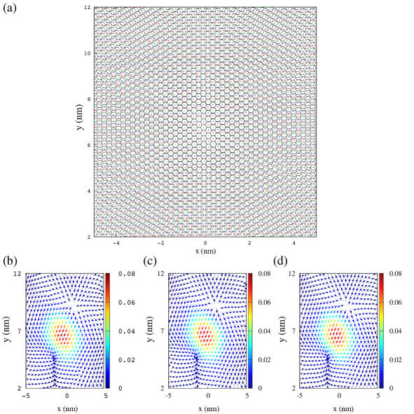
The current on the top layer is averaged at the center of each hexagonal plaquette. To avoid double counting of the atomic sites, we average over the centers of every third hexagonal plaquette which form a triangular lattice with lattice parameter , where is the carbon-carbon distance. To cover up the top layer, we have three different possible triangular lattices. These are identified in Fig. 15 (a) by the symbols , and . We used these lattices to define the current for each in the hexagonal plaquettes of the top layer as:
(8) -
•
The current in the bottom layer, , is averaged using the same triangular lattice defined for the top layer, but this time we select the atomic sites within a radius :
(9)
Using the above procedure the coordinates of the top and bottom current are the same and we can proceed to calculate and .
To confirm that the results obtained do not (strongly) depend on triangular lattice used, we present the resulting magnetic current using the local definition in Fig. 15 (b) - (d). It is clearly appreciated that the enhanced counterflow current in AA-stacked regions remains a robust feature irrespective of details of the calculation method.
Perturbations
Lattice relaxation
Let us analyze in more detail the effect of lattice relaxation following the approach by Nam and Koshino.Nam17 ; NamErratum We first present the source to drain current for the relaxed lattice that we used to normalise the current maps in the main text. In Fig. 16 (a), we show the calculated current as function of the gate voltage for , .
Vacancies
Vacancies in graphene induce the formation of localised states that can perturb the current distribution.PhysRevB.82.165438 In our device with armchair edges, we observe a reduction in the value of the in-plane magnetic moment for the region between and . This is shown in Fig. 16 (b) for a density of 10% of vacancies in the top flake edges having considered 5 randomly distributed vacancy realizations. We observe that the overall in-plane magnetic moment is robust against vacancies
Zigzag edges
We finally present the results for the TBG barrier embedded on top of a zigzag nanoribbon. For large angles, both layers are decoupled and the conductance is the same as the conductance of the single monolayer with zigzag edges. However, compared with armchair case the Fabry-Perot oscillation are more pronounced, see Fig. 17 (a). Similar to the armchair case, we observe a high DOS at the CNP. Also, the local DOS at this energy shows wavefunction localisation on the AA-stacked regions.
Spatial Distribution of Currents in Twisted Bilayer Graphene in the Continuum Model
Here we discuss the spatial distribution of currents induced by the adiabatic introduction of a uniform vector potential along the negative axis acting only on the layer 2, within the continuum model of Lopes dos Santos et al.Lopes07 The transient electric field points towards the positive axis and is therefore restricted to the layer 2, but currents are generated in both layers. We expect this asymmetric driving to best mimic the scattering calculation of the main text, even though the geometry differs: here the calculation corresponds to an infinite system. The twist angle is and the intra and interlayer hopping parameters are given by eV and eV (the value quoted for in the SI of Ref. Stauber18 should be divided by ). The calculation is standard linear response for the continuum modelStauber18 , adapted to obtain the response current at position , given by
| (10) |
where are pseudospin (current) operators. The calculation is restricted to Fermi levels within the lowest electron and hole bands around the neutrality point. Main results are:
1) The current is largest in the AA-stacked region, and opposite in both layers with near cancellation, as expected from previous workStauber18 ; Stauber18b . This is a generic property of the considered bands, as shown in Fig. 18, where the currents averaged for Fermi levels spanning the lowest electron and hole bands is presented.
2) The near cancellation makes the counterflow (magnetic) current, , to be largely enhanced in the AA-stacked regions as compared to the total current, . This is shown in Fig. 19 where the counterflow current exceeds the total current by three orders of magnitude. In fact, this is a conservative estimate because Fig. 19 represents the band average whereas the enhancement factor can be nominally infinite at the Dirac point, where the total current should vanish but the counterfow does notStauber18 ; Stauber18b .
3) We have also mimicked the presence of lattice relaxation by a -percent weakening of the AA interlayer hopping as compared to the AB one in the continuum model. The previous conclusions are hardly affected by this change, as shown in Fig. 20 where the counterflow currents are represented for both the undistorted and distorted cases.
All these features agree with the main message of this work: enhanced counterflow in AA-stacked regions close to the magic angle. It is interesting to remark that, although the total current flows in the positive -direction, which coincides with the (transient) electric field as expected, the current in the layer where the field is applied (layer 2) runs opposite to the field, see right panel of Fig. 18. This fact is at the heart of the large paramagnetic response previously reported.Stauber18 ; Stauber18b
References
- [1] J. M. B. Lopes dos Santos, N. M. R. Peres, and A. H. Castro Neto. Graphene bilayer with a twist: Electronic structure. Phys. Rev. Lett., 99(25):256802, Dec 2007.
- [2] E. Suárez Morell, J. D. Correa, P. Vargas, M. Pacheco, and Z. Barticevic. Flat bands in slightly twisted bilayer graphene: Tight-binding calculations. Phys. Rev. B, 82:121407(R), Sep 2010.
- [3] Rafi Bistritzer and Allan H. MacDonald. Moiré bands in twisted double-layer graphene. P. Natl. Acad. Sci. Usa., 108(30):12233–12237, 2011.
- [4] Pilkyung Moon and Mikito Koshino. Energy spectrum and quantum hall effect in twisted bilayer graphene. Phys. Rev. B, 85:195458, May 2012.
- [5] P. San-Jose, J. González, and F. Guinea. Non-abelian gauge potentials in graphene bilayers. Phys. Rev. Lett., 108:216802, May 2012.
- [6] D. Weckbecker, S. Shallcross, M. Fleischmann, N. Ray, S. Sharma, and O. Pankratov. Low-energy theory for the graphene twist bilayer. Phys. Rev. B, 93:035452, Jan 2016.
- [7] Yuan Cao, Valla Fatemi, Shiang Fang, Kenji Watanabe, Takashi Taniguchi, Efthimios Kaxiras, and Pablo Jarillo-Herrero. Unconventional superconductivity in magic-angle graphene superlattices. Nature, 556:43 EP –, 03 2018.
- [8] Matthew Yankowitz, Shaowen Chen, Hryhoriy Polshyn, Yuxuan Zhang, K. Watanabe, T. Taniguchi, David Graf, Andrea F. Young, and Cory R. Dean. Tuning superconductivity in twisted bilayer graphene. Science, 2019.
- [9] Satoshi Moriyama, Yoshifumi Morita, Katsuyoshi Komatsu, Kosuke Endo, Takuya Iwasaki, Shu Nakaharai, Yutaka Noguchi, Yutaka Wakayama, Eiichiro Watanabe, Daiju Tsuya, Kenji Watanabe, and Takashi Taniguchi. Observation of superconductivity in bilayer graphene/hexagonal boron nitride superlattices. arXiv:1901.09356.
- [10] Emilio Codecido, Qiyue Wang, Ryan Koester, Shi Che, Haidong Tian, Rui Lv, Son Tran, Kenji Watanabe, Takashi Taniguchi, Fan Zhang, Marc Bockrath, and Chun Ning Lau. Correlated insulating and superconducting states in twisted bilayer graphene below the magic angle. Science Advances, 5(9), 2019.
- [11] Cheng Shen, Na Li, Shuopei Wang, Yanchong Zhao, Jian Tang, Jieying Liu, Jinpeng Tian, Yanbang Chu, Kenji Watanabe, Takashi Taniguchi, Rong Yang, Zi Yang Meng, Dongxia Shi, and Guangyu Zhang. Observation of superconductivity with tc onset at 12k in electrically tunable twisted double bilayer graphene. arXiv:1903.06952, 2019.
- [12] Xiaobo Lu, Petr Stepanov, Wei Yang, Ming Xie, Mohammed Ali Aamir, Ipsita Das, Carles Urgell, Kenji Watanabe, Takashi Taniguchi, Guangyu Zhang, Adrian Bachtold, Allan H. MacDonald, and Dmitri K. Efetov. Superconductors, orbital magnets and correlated states in magic-angle bilayer graphene. Nature, 574(7780):653–657, 2019.
- [13] Yuan Cao, Valla Fatemi, Ahmet Demir, Shiang Fang, Spencer L. Tomarken, Jason Y. Luo, Javier D. Sanchez-Yamagishi, Kenji Watanabe, Takashi Taniguchi, Efthimios Kaxiras, Ray C. Ashoori, and Pablo Jarillo-Herrero. Correlated insulator behaviour at half-filling in magic-angle graphene superlattices. Nature, 556:80 EP –, 03 2018.
- [14] Youngjoon Choi, Jeannette Kemmer, Yang Peng, Alex Thomson, Harpreet Arora, Robert Polski, Yiran Zhang, Hechen Ren, Jason Alicea, Gil Refael, Felix von Oppen, Kenji Watanabe, Takashi Taniguchi, and Stevan Nadj-Perge. Electronic correlations in twisted bilayer graphene near the magic angle. Nature Physics, 15(11):1174–1180, 2019.
- [15] C. R. Dean, L. Wang, P. Maher, C. Forsythe, F. Ghahari, Y. Gao, J. Katoch, M. Ishigami, P. Moon, M. Koshino, T. Taniguchi, K. Watanabe, K. L. Shepard, J. Hone, and P. Kim. Hofstadter’s butterfly and the fractal quantum hall effect in moirésuperlattices. Nature, 497:598 EP –, 05 2013.
- [16] Kyounghwan Kim, Ashley DaSilva, Shengqiang Huang, Babak Fallahazad, Stefano Larentis, Takashi Taniguchi, Kenji Watanabe, Brian J. LeRoy, Allan H. MacDonald, and Emanuel Tutuc. Tunable moiré bands and strong correlations in small-twist-angle bilayer graphene. Proceedings of the National Academy of Sciences, 114(13):3364–3369, 2017.
- [17] Aaron L. Sharpe, Eli J. Fox, Arthur W. Barnard, Joe Finney, Kenji Watanabe, Takashi Taniguchi, M. A. Kastner, and David Goldhaber-Gordon. Emergent ferromagnetism near three-quarters filling in twisted bilayer graphene. Science, 365(6453):605–608, 2019.
- [18] Nick Bultinck, Shubhayu Chatterjee, and Michael P Zaletel. Anomalous hall ferromagnetism in twisted bilayer graphene. arXiv preprint arXiv:1901.08110, 2019.
- [19] Ya-Hui Zhang, Dan Mao, and T. Senthil. Twisted bilayer graphene aligned with hexagonal boron nitride: Anomalous hall effect and a lattice model. Phys. Rev. Research, 1:033126, Nov 2019.
- [20] S. S. Sunku, G. X. Ni, B. Y. Jiang, H. Yoo, A. Sternbach, A. S. McLeod, T. Stauber, L. Xiong, T. Taniguchi, K. Watanabe, P. Kim, M. M. Fogler, and D. N. Basov. Photonic crystals for nano-light in moiré graphene superlattices. Science, 362(6419):1153–1156, 2018.
- [21] Cheol-Joo Kim, Sánchez-Castillo A., Zack Ziegler, Yui Ogawa, Cecilia Noguez, and Jiwoong Park. Chiral atomically thin films. Nat. Nanotechnol., 11(6):520–524, 06 2016.
- [22] Ya-Hui Zhang, Dan Mao, Yuan Cao, Pablo Jarillo-Herrero, and T. Senthil. Nearly flat chern bands in moiré superlattices. Phys. Rev. B, 99:075127, Feb 2019.
- [23] Ya-Hui Zhang, Dan Mao, and T. Senthil. Twisted bilayer graphene aligned with hexagonal boron nitride: Anomalous hall effect and a lattice model. Phys. Rev. Research, 1:033126, Nov 2019.
- [24] Yu-Ping Lin and Rahul M. Nandkishore. Chiral twist on the high- phase diagram in moiré heterostructures. Phys. Rev. B, 100:085136, Aug 2019.
- [25] Laura Classen, Carsten Honerkamp, and Michael M. Scherer. Competing phases of interacting electrons on triangular lattices in moiré heterostructures. Phys. Rev. B, 99:195120, May 2019.
- [26] Vladyslav Kozii, Hiroki Isobe, Jörn W. F. Venderbos, and Liang Fu. Nematic superconductivity stabilized by density wave fluctuations: Possible application to twisted bilayer graphene. Phys. Rev. B, 99:144507, Apr 2019.
- [27] Tobias Stauber and Heinerich Kohler. Quasi-flat plasmonic bands in twisted bilayer graphene. Nano Lett., 16(11):6844–6849, 2016.
- [28] T. Stauber, T. Low, and G. Gómez-Santos. Chiral response of twisted bilayer graphene. Phys. Rev. Lett., 120:046801, Jan 2018.
- [29] T. Stauber, T. Low, and G. Gómez-Santos. Linear response of twisted bilayer graphene: Continuum versus tight-binding models. Phys. Rev. B, 98:195414, Nov 2018.
- [30] Cyprian Lewandowski and Leonid Levitov. Intrinsically undamped plasmon modes in narrow electron bands. Proceedings of the National Academy of Sciences, 116(42):20869–20874, 2019.
- [31] D Weckbecker, M Fleischmann, R Gupta, W Landgraf, S Leitherer, O Pankratov, S Sharma, V Meded, and S Shallcross. Moir’e ordered current loops in the graphene twist bilayer. arXiv:1901.04712, 2019.
- [32] J. González and T. Stauber. Kohn-luttinger superconductivity in twisted bilayer graphene. Phys. Rev. Lett., 122:026801, Jan 2019.
- [33] J. González and T. Stauber. Marginal fermi liquid in twisted bilayer graphene. arXiv:1903.01376.
- [34] Stephen Carr, Daniel Massatt, Shiang Fang, Paul Cazeaux, Mitchell Luskin, and Efthimios Kaxiras. Twistronics: Manipulating the electronic properties of two-dimensional layered structures through their twist angle. Phys. Rev. B, 95:075420, Feb 2017.
- [35] Xiaomeng Liu, Zeyu Hao, Eslam Khalaf, Jong Yeon Lee, Kenji Watanabe, Takashi Taniguchi, Ashvin Vishwanath, and Philip Kim. Spin-polarized correlated insulator and superconductor in twisted double bilayer graphene. arXiv:1903.08130, 2019.
- [36] Yuan Cao, Daniel Rodan-Legrain, Oriol Rubies-Bigorda, Jeong Min Park, Kenji Watanabe, Takashi Taniguchi, and Pablo Jarillo-Herrero. Electric field tunable correlated states and magnetic phase transitions in twisted bilayer-bilayer graphene. arXiv:1903.08596, 2019.
- [37] Guorui Chen, Aaron L. Sharpe, Patrick Gallagher, Ilan T. Rosen, Eli J. Fox, Lili Jiang, Bosai Lyu, Hongyuan Li, Kenji Watanabe, Takashi Taniguchi, Jeil Jung, Zhiwen Shi, David Goldhaber-Gordon, Yuanbo Zhang, and Feng Wang. Signatures of tunable superconductivity in a trilayer graphene moirésuperlattice. Nature, 572(7768):215–219, 2019.
- [38] G. Trambly de Laissardière, D. Mayou, and L. Magaud. Localization of dirac electrons in rotated graphene bilayers. Nano Letters, 10(3):804–808, 2010.
- [39] G. Trambly de Laissardière, D. Mayou, and L. Magaud. Numerical studies of confined states in rotated bilayers of graphene. Phys. Rev. B, 86:125413, Sep 2012.
- [40] Xiaomeng Liu, Kenji Watanabe, Takashi Taniguchi, Bertrand I. Halperin, and Philip Kim. Quantum hall drag of exciton condensate in graphene. Nature Physics, 13:746 EP –, 05 2017.
- [41] I. Brihuega, P. Mallet, H. González-Herrero, G. Trambly de Laissardière, M. M. Ugeda, L. Magaud, J. M. Gómez-Rodríguez, F. Ynduráin, and J.-Y. Veuillen. Unraveling the intrinsic and robust nature of van hove singularities in twisted bilayer graphene by scanning tunneling microscopy and theoretical analysis. Phys. Rev. Lett., 109:196802, Nov 2012.
- [42] D. A. Bahamon, A. H. Castro Neto, and Vitor M. Pereira. Effective contact model for geometry-independent conductance calculations in graphene. Phys. Rev. B, 88:235433, Dec 2013.
- [43] Henning Schomerus. Effective contact model for transport through weakly-doped graphene. Phys. Rev. B, 76:045433, Jul 2007.
- [44] A. Luican, Guohong Li, A. Reina, J. Kong, R. R. Nair, K. S. Novoselov, A. K. Geim, and E. Y. Andrei. Single-layer behavior and its breakdown in twisted graphene layers. Phys. Rev. Lett., 106:126802, Mar 2011.
- [45] L. Chico and W. Jaskólski. Localized states and conductance gaps in metallic carbon nanotubes. Phys. Rev. B, 69:085406, Feb 2004.
- [46] S. Datta. Electronic Transport in Mesoscopic Systems. Cambridge University Press, 1995.
- [47] Michael Walz, Jan Wilhelm, and Ferdinand Evers. Current patterns and orbital magnetism in mesoscopic dc transport. Phys. Rev. Lett., 113:136602, Sep 2014.
- [48] C. J. Páez, D. A. Bahamon, and Ana L. C. Pereira. Current flow in biased bilayer graphene: Role of sublattices. Phys. Rev. B, 90:125426, Sep 2014.
- [49] Katsunori Wakabayashi. Electronic transport properties of nanographite ribbon junctions. Phys. Rev. B, 64:125428, Sep 2001.
- [50] Yi Liu and Hong Guo. Current distribution in b- and n-doped carbon nanotubes. Phys. Rev. B, 69:115401, Mar 2004.
- [51] O. Entin-Wohlman, Y. Imry, A. G. Aronov, and Y. Levinson. Orbital magnetization in the hopping regime. Phys. Rev. B, 51:11584–11596, May 1995.
- [52] Shousuke Nakanishi and Masaru Tsukada. Quantum loop current in a molecular bridge. Phys. Rev. Lett., 87:126801, Aug 2001.
- [53] Naoto Tsuji, Shigehiro Takajo, and Hideo Aoki. Large orbital magnetic moments in carbon nanotubes generated by resonant transport. Phys. Rev. B, 75:153406, Apr 2007.
- [54] Nguyen N. T. Nam and Mikito Koshino. Lattice relaxation and energy band modulation in twisted bilayer graphene. Phys. Rev. B, 96:075311, Aug 2017.
- [55] Nguyen N. T. Nam and Mikito Koshino. Erratum: Lattice relaxation and energy band modulation in twisted bilayer graphene [phys. rev. b 96, 075311 (2017)]. Phys. Rev. B, 101:099901, Mar 2020.
- [56] Procolo Lucignano, Dario Alfè, Vittorio Cataudella, Domenico Ninno, and Giovanni Cantele. Crucial role of atomic corrugation on the flat bands and energy gaps of twisted bilayer graphene at the magic angle . Phys. Rev. B, 99:195419, May 2019.
- [57] Fernando Gargiulo and Oleg V Yazyev. Structural and electronic transformation in low-angle twisted bilayer graphene. 2D Materials, 5(1):015019, nov 2017.
- [58] Sandeep K Jain, Vladimir Juričić, and Gerard T Barkema. Structure of twisted and buckled bilayer graphene. 2D Materials, 4(1):015018, nov 2016.
- [59] L. P. Zârbo and B. K. Nikolić. Spatial distribution of local currents of massless dirac fermions in quantum transport through graphene nanoribbons. Europhysics Letters (EPL), 80(4):47001, oct 2007.
- [60] H. Zhou, H. Polshyn, T. Taniguchi, K. Watanabe, and A. F. Young. Solids of quantum hall skyrmions in graphene. Nature Physics, 16(2):154–158, 2020.
- [61] Tian-Heng Han, Joel S. Helton, Shaoyan Chu, Daniel G. Nocera, Jose A. Rodriguez-Rivera, Collin Broholm, and Young S. Lee. Fractionalized excitations in the spin-liquid state of a kagome-lattice antiferromagnet. Nature, 492:406 EP –, 12 2012.
- [62] AV Chumak, VI Vasyuchka, AA Serga, and Burkard Hillebrands. Magnon spintronics. Nature Physics, 11(6):453, 2015.
- [63] J. W. González, H. Santos, E. Prada, L. Brey, and L. Chico. Gate-controlled conductance through bilayer graphene ribbons. Phys. Rev. B, 83:205402, May 2011.
- [64] J. Tworzydło, B. Trauzettel, M. Titov, A. Rycerz, and C. W. J. Beenakker. Sub-poissonian shot noise in graphene. Phys. Rev. Lett., 96:246802, Jun 2006.