Enhanced energy transfer via graphene–coated wire surface plasmons
Abstract
This work analyzes the electromagnetic energy transfer rate between donor and acceptor quantum emitters close to a graphene–coated wire. We discuss the modification of the energy transfer rate when the emitters are interfaced via surface plasmon (SP) environments. All of the notable effects on the spatial dependence of the energy transfer are highlighted and discussed in terms of SP propagation characteristics. Our results show that a dramatically enhancement of the energy transfer occur when the graphene wire SPs are excited. Moreover, different dipole moment orientations influence differently this enhancement. As a consequence of the quasi–one–dimensional graphene wire SPs, we found that the normalized energy transfer rate reaches a maximum value at a donor–acceptor distance which is twice the value corresponding to its two–dimensional counterpart consisting of a single graphene sheet or a flat graphene waveguide. In particular, we provide a simplified model that reproduces the main features of the numerical results.
keywords:
electromagnetic energy transfer , graphene , plasmonicsPACS:
81.05.ue , 73.20.Mf , 78.68.+m , 42.25.Fx1 Introduction
The potential of SPs to confine the electromagnetic field to regions well below the diffraction limit has been widely exploited to manipulate the light–matter interaction at subwavelength scales enabling a rich variety of applications [1, 2, 3]. In particular, the coupling of optical emitters, such as atoms, molecules or quantum dots, to SP modes provides an enhancement of the emission rate several orders of magnitude relative to the case in which the same emitter is localized in an unbounded medium. This property has been used to bring the size of laser sources of light to the nanoscale, to reduce the lasing threshold [4, 5] as well as to improve the efficiency of single photon sources [6]. In addition, SP mode environments can provide an enhancement together a significant directional control of the energy transfer between quantum emitters over distances larger than the Förster energy transfer range [7, 8, 9, 10, 11].
Significant progress made in nanoscale fabrication techniques and an extensive wealth of theoretical analysis have not only allowed an advanced light manipulation via SPs at optical frequencies (where optical emitters are placed on metallic SP environments), but have also led to a rapidly developing field in light control by plasmonic excitation in the terahertz (THz) frequency range [12]. Possibilities have been widened with the advent of other plasmonic materials with lower losses and greater confinement of the electromagnetic field, such as metal–alloys, heavily doped wide–band semiconductors, and graphene [13]. Due to their unique property to guide SPs by one–atom–thin layer from microwaves to the mid–infrared regimes [14, 15, 16], graphene has attracted significant interest from the nanophotonics research community. The electronic linear band structure of graphene makes a SP mass depending on the Fermi–level position and consequently electrically tunable and long–lived SPs are supported by graphene.
One of the major challenges for most of applications is to build more smaller plasmonic constituent elements to control light at subwavelength scales, in particular from microwaves to the mid–infrared regimes which comprises a crossover between electronic and optics. In this way, graphene–plasmonic has found a great variety of sophisticated applications, such as photonic devices capable to achieve invisibility [17, 18], electrically tunable THz antennas [19, 20, 21, 22] and efficient THz waveguides [23]. The propagation characteristics of graphene plasmonic waveguides have been investigated in different geometrical structures, such as planar waveguides [24, 25, 26] ribbons [27, 28], grooves [29] and graphene–cylinders with circular cross–section [30]. The ability of plasmonic graphene wires to guide light confined well below the diffraction limit has the key advantage for tailoring light–matter interactions [31, 32], opening routes for novel electrically controllable devises capable to improve the single emitter emission as well as the energy transfer rate between optical emitters [33, 34, 35, 36, 37, 38].
Methods for controlling the relative positions of single emitters and SP wires with high experimental accuracy have been reported. In [39], it was described the use of electron beam lithography to create a polymer template that enables the controlled deposition of a small number of quantum dots in areas that measure about 50nm across. Alternatively, in [40] the authors have reported the use of a microfluidic device for positioning at desired locations and moving quantum dots around a single metallic nanowire with a 12nm spatial accuracy.
This paper deals with the study about the energy transfer rate between single emitters, a donor and acceptor, located near a graphene–coated wire. In a recent work [41], we have revealed that the interplay between an optical emitter and SP excitations on a graphene layer strongly influences the energy transfer process between two single optical emitters placed close to a graphene–coated cylinder. However, in that work we have focused on a two–dimensional model in which each of the optical emitters is considered as an infinitely thin wire extending along the axis of the cylinder and with its dipole moment in the computational plane. As a consequence, only localized surface plasmons, i.e., SPs whose wave vector component along the wire axis is equal to zero, are excited, leading to an optical energy transfer from donor to acceptor within the plane.
Our motivation for this work is to extend the study realized in [41] to the case of quantum dot optical emitters. Unlike the two–dimensional approach, SPs propagating along the waveguiding structure, i.e., SPs with a non null wave vector component along the wire axis, are excited and consequently the energy can be transferred between two distant optical emitters placed near the graphene–wire at a distance from each other. In this sense, the present work can be considered as an extension to the cylindrical geometry case of our previous study about the effect of SPs on the resonant energy transfer on a planar graphene waveguide [42].
This paper is organized as follows. In section 2, we sketch the boundary–value problem for the diffraction problem of a dipole emitter located in close proximity to a graphene–coated wire. Because of the translational symmetry of the system along the direction of the wire axis, the transverse components of the electromagnetic fields are obtained from their longitudinal components for which we derive integral expressions for the scattered fields. We then include a second dipole emitter and deal with the problem of the coupled system. By using contour integration in the complex plane, we have applied a method developed in Ref. [42] to perform the field integration. This method which is based on the residues theorem enables a fast calculation of the contribution of each one of the wire modes to the energy transfer rate. In section 3 we present numerical results obtained under different dipole moment configurations. Concluding remarks are provided in Section 4. The Gaussian system of units is used and an time–dependence is implicit throughout the paper, where is the angular frequency, is the time coordinate, and . The symbols Re and Im are used for denoting the real and imaginary parts of a complex quantity, respectively.
2 Theory
We consider the energy transfer rate between a donor D and an acceptor A electric dipoles placed close to a graphene–coated wire, as illustrated in Figure 1. The energy transfer in the presence of the graphene–coated wire normalized to that in an unbounded medium 1 (without graphene waveguide), is given by [43]
| (1) |
where the electric field is the electric field in the presence of a graphene–coated wire (see A), is due to an electric dipole in an unbounded medium (see B), is a unit vector along the induced polarization of the acceptor (whose direction is assumed to be fixed) and is the position of the acceptor.
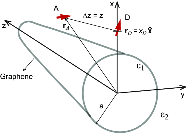
We consider the case in which the donor is placed outside the graphene–coated wire (). Without loss of generality we choose , i.e. the donor position as shown in Figure 1. By using Eqs. (A), (B14) and (B13) we obtain the transverse components of the scattered electric field for ,
| (2) |
and
| (3) |
where the complex amplitudes and are given by expressions (B22) and (B23), respectively. The integration path in Eqs. (2) and (2) is set along the real axis and poles, i.e., zeroes of the denominator in and amplitudes, close to that axis give rise to poor numerical convergence. To avoid this difficulty we have applied a method developed in Ref. [42] to perform such integration which requires the application of the residues theorem to extract each pole contribution of the integrals (2) and (2).
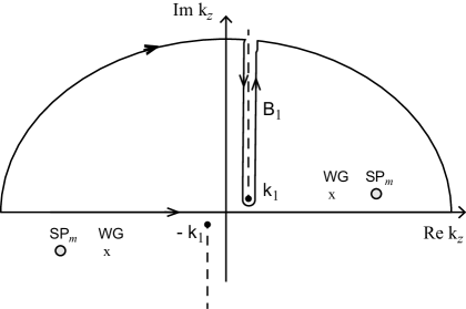
In order to perform the calculation of these pole contributions to the field, we deform the integration path in (2) and (2) into a semicircle of large radius () avoiding the branch point and pole singularities. If the contour of integration is deformed to the upper–half plane (see Figure 2) whereas, if the contour of integration is deformed to the lower–half plane . The integration along the branch cut results in a volume wave [44, 45], which consist of a continuous spectrum of radiation modes. Here, we focus on distances between emitters of the same order than the propagation length of the graphene wire eigenmodes, thus the intensity of the electric field reached by the excitation of these modes dominates the energy transfer process and the volume wave mode contribution can be neglected. Then, the application of the residues theorem to Eqs. (2), (2) and (B14) gives the following components of the scattered fields
| (4) |
| (5) |
| (6) |
where is the propagation constant of a particular eigenmode, and Res is the residue of the integrand in (2), (2) and (B14) at the pole .
Inserting the expressions for into Eq. (1) we obtain the following expression for the normalized energy transfer rate,
| (8) |
where
| (9) |
The terms in the first sum in Eq. (8) represent the contribution of each of the eigenmode channels to the normalized energy transfer rate whereas each term in the second sum arises from the interference between and mode channels,
| (10) |
3 Results
In this section, we apply the formalism sketched in previous section to calculate the energy transfer rate between two emitters localized close to a graphene–coated wire. In all the calculations we assume that the core is made of a transparent material with constitutive parameters (corresponding to Polymethylpentene) and is embedded in vacuum (). In order to obtain separate contributions of different SP modes, firstly the propagation constant of these modes are obtained by requiring the denominator in the amplitudes and to be zero (see A),
| (11) |
where () and , . This condition is the dispersion relation of SPs and it determines the complex propagation constant in terms of all the parameters of the graphene–coated wire. Equation (11) has complex solutions with the same modulus and opposite signs, corresponding to SP propagation along the directions . We have found the complex roots of equation (11) by adapting a numerical code based on Newton Raphson method. In our examples we have selected the solution with corresponding to wave propagation along the direction.
In the case, Eq. (11) is decoupled into two independent equations: an equation whose solutions have the longitudinal component of the magnetic field (TM polarization),
| (12) |
and another equation whose solutions have the longitudinal component of the electric field (TE polarization),
| (13) |
In the limit , taking into account the asymptotic expressions of the Bessel and Hankel functions [48], the dispersion equation (12) converges to the TM dispersion equation of a single graphene sheet [23]
| (14) |
whereas Eq. (13) converges to the TE dispersion equation of a single graphene sheet
| (15) |
In the general case , the modes are not decomposed into independent polarizations, and to calculate the propagation constant of these modes we must solve Eq. (11).
As in the planar waveguides case, the energy transfer through the graphene–coated wire due to excitation of SPs is much greater than the corresponding energy transfer through the excitation of wave guided modes (modes which are evanescent outside the graphene–coated wire and standing waves in the insulator core) [26, 42]. This is true because graphene SP modes are highly localized in comparison with waveguide (or fiber) modes [30]. In addition, –polarized SPs only exist for frequencies such as where the imaginary part of the graphene conductivity is negative (see appendix C). For frequencies bellow this value, , (the frequency range studied in this work) only –polarized SPs are well defined. Thus, as we have verified, the –polarized SP modes contributions dominate the energy transfer process on the frequency region presented in figure 3 and consequently all other mode contributions, which are solution of Eq. (11), can be neglected in equation (8).
Figure 3 shows the propagation constant () of SPs as a function of the frequency for m. The Kubo parameters are eV, meV and K. With this value of , –polarized SPs are supported by the graphene wire for frequency values less than m-1. These figures also show the curves corresponding to the propagation constant of SPs supported by a single graphene sheet interface (dotted line), i.e., a system with the flat graphene sandwiched between two dielectric half space with permittivities and , calculated by solving Eq. (14).
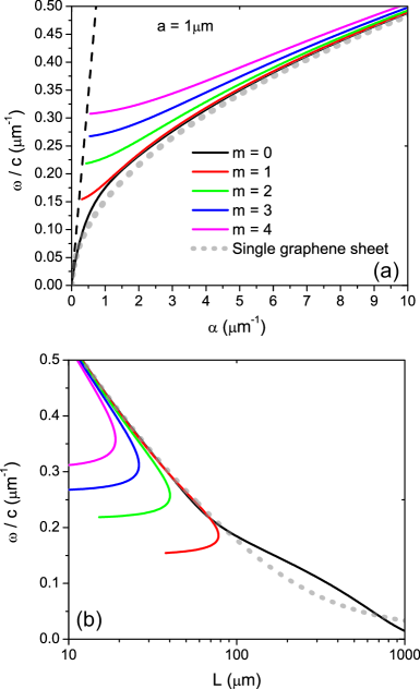
From Figure 3a we see that SP curves exist to the right of the light line of the inner dielectric medium. As in the metallic wire case [3], the mode goes down to approaching the light line from the right. The modes with intersects the light line at a finite value. Figure 3b shows the propagation length of the SPs calculated as . For frequency values large enough, both functions and take a value which is almost equal to that of the single graphene sheet interface.
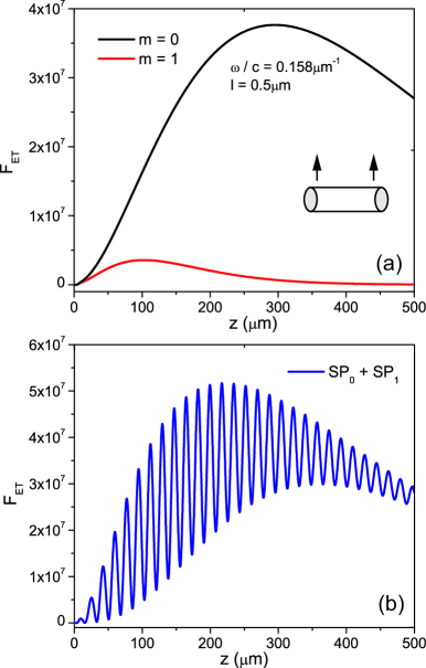
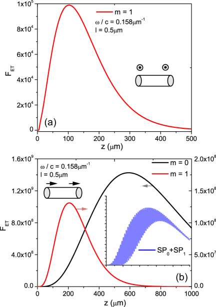
Once the SP propagation constants are calculated, the contribution of each modes to the energy transfer rate between donor and acceptor can be obtained by using Eq. (9). To illustrate the interesting case where the coherent interference between these SP channels leads to large spatial variations, we chose a frequency value for which two of the plasmonic bands plotted in Figure 3 show a significant difference in their propagation constant values. Figure 4 shows the contribution of SP0 and SP1 modes (SP modes with and ) to the energy transfer rate ( with and ) as a function of the separation between the donor and acceptor and for m-1. The locations are m and m for the donor and acceptor, respectively, and both dipole moments are aligned along the direction (the directions of the dipole moments are shown in the graphs by the directions of the arrows). As can be seen in Figure 3, only SPs with and are propagating and as a consequence only these modes carry energy through the graphene wire. Figure 4a shows that the energy transfer contribution curves reach a maximum value for a certain value of the separation, m for the SP0 mode and m for the SP1 mode. On the other hand, from Figure 3b we determine the propagation lengths of SP modes resulting: m for the SP0 mode and m for the SP1 mode. This result suggests that the maximum contributions to the total normalized energy transfer rate are reached at a distance, between the donor and acceptor, two times larger than the SP propagation lengths. This fact can be understood as follows: due to the –component of the SP electric field (2) depends on the distance as , and the fact that in the absence the graphene wire, the field of the donor is written as (refer to B for its derivation) , it follows that the energy transfer contribution of either of the two SP channels (2) can be written as
| (16) |
which reaches its maximum value at . It is worth noting that, if the same donor–acceptor configuration (where both donor and acceptor dipole moments are oriented perpendicularly to the graphene surface) is placed near a planar graphene system, such as a single graphene sheet or a planar graphene waveguide, then the maximum energy transfer value is reached at a donor–acceptor separation which coincides with the SP propagation length [42]. This difference lies in the geometry of the system through which the energy emitted by the donor dipole travels. As its required by energy conservation, in the planar graphene case (2D case), the plasmonic energy amplitude is proportional to () whereas for the wire case (1D case) this amplitude is constant.
Figure 4b shows the energy transfer rate between the donor and acceptor as a coherent superposition of the SP0 and the SP1 contributions and calculated by using Eq. (8). Due to the presence of the interference term with and , this curve shows a pronounced spatial oscillation whose period m, a value that can be calculated within the framework of the model in Eq. (10), where the interference term between the SP0 and SP1 is written as
| (17) |
Equation (10) shows a periodic spatial dependence along direction with a period m, where we have used the values of the SP propagation constants calculated in Figure 3a for m-1.
We next consider the case where the two dipole moments are parallel to the surface of the cylinder but perpendicular to the axis of the cylinder, as shown in the inset in Figure 5a. Since the electric field component of the SP0 along the direction is zero [23], the plasmonic order is not coupled to the dipole incident field, and as a consequence the energy transfer contribution associated to this order is zero [we have numerically verified this assertion]. In Figure 5a we have plotted the energy transfer contribution of the SP1 mode. As in the previously presented case where the donor and acceptor dipole moments are perpendicular to the graphene cylinder, we also observe that the maximum normalized energy transfer rate is obtained for a value of the separation two times larger than the propagation length of the SP, m.
In Figure 5b we have plotted the energy transfer contribution for the case where the two dipole moments are parallel to the axis of the cylinder, . Unlike previous configurations, the distance m for the order and m for the order. These values represent fourfold the SP propagation length of the and orders. This fact can be understood by taking into account that, in the absence of the graphene cylinder, the component of the donor electric field for is written as (see B)
| (18) |
while the component of the SP electric field is as in Eq. (B14), . Thus, the energy transfer contribution of either of the two SP channels (6) can be written as
| (19) |
which reaches its maximum value at . Note that the values of the normalized energy transfer rate shown in Fig. 5b (donor–acceptor emitters with dipole moment oriented parallel to the wire axis) are approximately two orders of magnitude larger than that corresponding to perpendicular orientation plotted in Figs. 4 and 5a. This is true because the energy transfer rate without graphene wire decays as for donor–acceptor emitters oriented parallel to the wire axis whereas it decay as for other orientations of the emitters. In the inset in Figure 5b we plotted the curve corresponding to the energy transfer rate as a superposition of the SP0 and SP1 modes as a function of the separation between the donor and acceptor. This curve presents an oscillation whose spatial period is the same as in Figure 4b, m.
It is worth noting that the calculation of the energy transfer for small donor–acceptor separations () is a limitation of the presented model. At these distances, the contribution of the radiative modes, which are excluded in our model, is not negligible and our calculations depart significantly from experimental values. Since the emitter–SP coupling decreases with the emitter–cylinder distance, we expect this effect becomes even more pronounced when emitters are far away from the surface of the cylinder.
4 Conclusions
In conclusion, we have examined the energy transfer rate behavior from a donor to an acceptor close to a graphene–coated wire of circular cross section. We developed an analytical classical method and obtained a rigorous solution for the electromagnetic field in an integral form. By solving the eigenmodes dispersion equation, which is related to the study of the non–trivial solutions to the boundary value problem in the absence of external sources, we have obtained the complex propagation constants of the graphene–wire SPs. This allowed us to calculate the contribution of each of these SPs to the total energy transfer rate.
In all the presented examples, we have provide a comprehensive analysis about the strong impact of SPs on the energy transfer rate between two single emitters in terms of their kinematic characteristics. Our calculations show that the SP maximum contribution to the total normalized energy transfer is reached when the donor–acceptor distance is twice the value of the SP propagation length for the configuration when both dipole moments are oriented perpendicular to the wire axis. This result differ from that obtained for planar graphene systems, such as a single graphene sheet or a planar graphene waveguide for which the maximum energy transfer value is reached at a donor–acceptor separation which coincides with the SP propagation length. In case where the dipole moments of both the donor and acceptor are parallel to the wire axis, these maximum contributions are reached at a distance four times larger than the SP propagation lengths.
In addition, we have obtained a simple relation, which uses the SP dispersion relation, that allows us to calculate the spatial dependence of the normalized energy transfer rate between two quantum emitters. Although in our examples only it is consider three polarization directions, the method described in section 2 allows to calculate the energy transfer regarding an arbitrary dipole moment orientation in relation to the graphene–coated wire. In particular, from the presented results it can be inferred that, for an arbitrary orientation of the dipole moments, each of the modal plasmonic contributions to the normalized energy transfer rate will have two characteristic lengths related with the propagation length of the SPs involved.
Finally, the research can be continued by considering graphene–coated wire with a finite lenght. In this case, reflections at the wire facets modify the dispersion relation of SPs playing a key role in the energy transfer process. A simple semi–analytical approach used in case of a metallic wire [51] considers the field confinement in the transverse wire direction and reflections at the wire ends as two completely independent problems. This procedure leads to dispersion curves of an infinite cylinder but with an intermode spacing which is proportional to the inverse wire length (Fabry–Perot modes). A most rigorous approach that could be applied to the graphene–coated wire takes into account the formulation of the equivalence theorem to obtain a dispersion relation of the Fabry–Perot modes [52]. As a result of applying these two approaches, the energy transfer rate would be enhanced at the frequencies corresponding to Fabry–Perot modes. Although we could planning such study in a future, as a first step, we believe that our contribution can be valuable for experimentalist, which using the dispersion relation of SPs, can calculate the interaction distance between a pair of quantum emitters by using a simple relation.
Acknowledgment
The authors acknowledge the financial support of Consejo Nacional de Investigaciones Científicas y Técnicas (CONICET). Discussions with Vasilios Karanikolas (Materials Science Department, School of Natural Sciences, University of Patras, Patras, Greece) are gratefully acknowledged.
Appendix A Electric field of a dipole in presence of a graphene–coated wire
We consider an electric dipole p localized at , at a distance from the center of the cylindrical wire. The current density of the electric dipole is
| (B1) |
In an unbounded medium (constitutve parameters , ), the dipole vector potential is
| (B2) |
where , is the modulus of the photon wave vector in vacuum, is the angular frequency, is the vacuum speed of light, is the electric permittivity and the superscript denotes medium 2. In order to take advantage of the translational symmetry of the system along direction, we expand Eq. (B2) into cylindrical eigenfunctions,
| (B3) |
where the subscript denotes , or , , () is the smaller (larger) of and , is the component of the electric dipole and and are the nth Bessel and Hankel functions of the first kind, respectively. By using the equations
| (B4) |
| (B5) |
explicit expressions for the electric and magnetic fields emitted by the dipole are obtained
| (B6) |
| (B7) |
For , the complex amplitudes of the tangential fields and () are given by
| (B8) |
| (B9) |
| (B10) |
where the prime denotes the derivative with respect to the argument and . For we need to exchange and in equations (B8) to (A).
The component of the scattered electric and magnetic fields, denoted by and (), are expanded as a functions of cylindrical harmonics, one for the internal region (, superscript ) and another one for the external region (, superscript ),
| (B11) |
| (B12) |
| (B13) |
| (B14) |
where and () are unknown complex coefficients. Because of the cylindrical geometry, by combining the Faraday and Ampere–Maxwell equations [46] the transverse components of the electromagnetic fields () can be obtained from their longitudinal components and ,
| (B15) |
where is the transverse part of the operator. Due to the graphene coating, the tangential components of the magnetic field are no longer continuous across the boundary as they were in the case of uncoated cylinders. Considering this, the boundary conditions on the interface impose that
| (B16) |
Inserting the expressions of the tangential components of the incident and scattered fields into the boundary conditions, we obtain a system of equations for the amplitudes of the scattered fields,
| (B17) |
where and . It is worth noting that the dipole field amplitudes , , and have been evaluated at . Note that, in the case of , i.e., in the absence of current density induced in the graphene wrapping, Eq. (B17) converges to the standard boundary conditions without graphene [47]. The coefficients and are eliminated from Eqs. (B17) and a system of equations for the coefficients and is obtained,
| (B18) |
Appendix B Electric field of a dipole in an unbounding medium
We consider an electric dipole at position oriented along direction, . The vector potential in spherical coordinates is given by [43]
| (A1) |
where . By using Eqs. (B4) and (B5), we obtain the following components for the electric field in cartesian coordinates
| (A7) |
For the electric dipole orientation along the direction, , the field components can be obtained from Eqs. (A7) by replacing , , and .
Appendix C Graphene conductivity
We consider the graphene layer as an infinitesimally thin, local and isotropic two–sided layer with frequency–dependent surface conductivity given by the Kubo formula [49, 50], which can be read as , with the intraband and interband contributions being
| (C1) |
| (C2) |
where is the chemical potential (controlled with the help of a gate voltage), the carriers scattering rate, the electron charge, the Boltzmann constant and the reduced Planck constant.
References
- [1] Tame M S, McEnery K R, Ozdemir K, Lee J, Maier S A and Kim M S, Nat. Phys. 9, (2013) 329–340
- [2] Weijia Wang, Mohammad Ramezani, Aaro I. Väkeväinen, Päivi Törmä, Jaime Gómez Rivas, Teri W. Odom, Materials Today 21, (2018)
- [3] J Barthes, A Bouhelier, A Dereux and G Colas des Francs, Scientific Reports 3, (2013) 2734
- [4] Oulton RF, Sorger VJ, Zentgraf T, Ren–Min Ma, Gladden C, Lun Dai, Bartal G and Zhang X, Nature 461 (2009)
- [5] Molina P, Yraola E, Ramírez MO, Tserkezis C, Plaza JL, Aizpurua J, Bravo–Abad J, and Bausaá LE, Nano Lett. 16, (2016) 895–899
- [6] Eisaman MD, Fan J, Migdall A and Polyakov SV, Rev. Sci. Instrum. 82, (2011) 071101
- [7] Medintz I.L., Hildebrandt N., Eds. FRET–Förster Resonance Energy Transfer. From Theory to Applications, Wiley–VCH, Weinheim, Germany (2013)
- [8] Andrew P. and Barnes W. L., Science 306, (2004) 1002
- [9] V Karanikolas, C A Marocico, A L Bradley, Physical Review A 89, (2014) 063817
- [10] Diego Martín–Cano, L Martín–Moreno, F J García–Vidal and E Moreno, Nano Lett. 0, (2010) 3129–3134
- [11] G. A. Jones and D. S. Bradshaw, Frontiers in Physics 7, (2019)
- [12] S. S. Dhillon, M. S. Vitiello, E. H. Linfield, A. G. Davies, M. C. Hoffmann, J. Booske, C. Paoloni, M. Gensch, P. Weightman, G. P. Williams, E. Castro-Camus, D. R. S. Cumming, F. Simoens, I. Escorcia-Carranza, .J Grant, S. Lucyszyn, M. Kuwata-Gonokami, K. Konishi, M. Koch, C. A. Schmuttenmaer, T. L. Cocker, R. Huber, A. G. Markelz, Z. D. Taylor, V. P. Wallace, J. A. Zeitler, J. Sibik, T. M. Korter, B. Ellison, S. Rea, P. Goldsmith, K. B. Cooper, R. Appleby, D. Pardo, P. G. Huggard, V. Krozer, H. Shams, M. Fice, C. Renaud, A. Seeds, A. Stöhr, M. Naftaly, N. Ridler, R. Clarke, J. E. Cunningham, and M. B. Johnston, J. Phys. D: Appl. Phys. 50, (2017) 043001
- [13] West P, Ishii S, Naik G, Emani N,Shalaev V, Boltasseva A, Searching for better plasmonic materials Laser Photon Rev 4, (2010) 795–808.
- [14] Fengnian Xia, Nature Photonics 7, (2013) 420
- [15] Garcia–Pomar, J. L., Nikitin, A. Y. and Martin–Moreno, L., ACS Nano 7, (2013) 4988–4994
- [16] Slipchenko, T., Nesterov, M. L., Hillenbrand, R., Nikitin, A. Y., Martin–Moreno, L., ACS Photonics 4 (2017), 3081–3088
- [17] Naserpour M., Zapata–Rodríguez C. J., Vukovic S. M., Pashaeiadl H. and Belic M. R., Sci. Rep. 7, (2017) 12186
- [18] Vitalii I. Shcherbinin, Yuliya K. Moskvitina, Volodymyr I. Fesenko, Vladimir R. Tuz, arXiv 1904.08556, (2019)
- [19] I Llatser, C Kremers, D N Chigrin, J M Jornet, M C Lemme, A Cabellos–Aparicio, E Alarcon, Radioengineering 21, (2012)
- [20] Filter R., Farhat M., Steglich M., Alaee R., Rockstuhl R. and Lederer F., Opt. Exp. 21, (2013) 3737
- [21] Tamagnone M., Gómez–Díaz J. S., Mosig J. R. and Perruisseau–Carrier J., Appl. Phys. Lett. 101, (2012) 214102
- [22] Cuevas M., Superlattices and Microstructures 122, (2018) 216–227
- [23] R A Depine, Graphene Optics: Electromagnetic solution of canonical problems, IOP Concise Physics. San Raefel, CA, USA: Morgan and Claypool Publishers, (2017)
- [24] Karanikolas V. D., Marocico C. A., and Bradley A. L., Phys. Rev. B 91, (2015) 125422
- [25] DA Smirnova, IV Iorsh, IV Shadrivov, YS Kivshar, JETP letters 99, (2014) 456–460
- [26] Cuevas M., J. Opt. 18, (2016) 105003
- [27] Nikitin AY, Guinea F, García–Vidal FJ, Martín–Moreno L., Phys Rev B 84, (2011) 161407
- [28] Christensen J, Manjavacas A, Thongrattanasiri S, Koppens FH, García de Abajo FL, ACSNano 6, (2012) 431–40
- [29] Liu P, Zhang X, Ma Z, Cai W, Wang L, Xu J, Opt Express 21, (2013) 32432–40
- [30] Artur R. Davoyan and Nader Engheta, ACS Photonics 3, (2016) 737–742
- [31] Vasilios Karanikolas, Pelin Tozman and Emmanuel Paspalakis, arXiv 1904.06740, (2019)
- [32] L. Martín–Moreno, F. J García de Abajo, and F. J. García–Vidal, Phys. Rev. Lett. 115, (2015) 173601
- [33] Biehs S.A., and Agarwal G. S., Appl. Phys. Lett. 103, (2013) 243112
- [34] Velizhanin K. A., Shahbazyan T. V., Phys. Rev. B 86, (2012) 245432
- [35] Arruda T. J., Bachelard R., Weiner J., Courteille P. W., Phys. Rev. B 98, (2018) 245419
- [36] Cuevas M., Journal of Quantitative Spectroscopy and Radiative Transfer 206, (2018) 157–162
- [37] T Bian, R Chang, PT Leung, Plasmonics 11, (2016) 1239–1246
- [38] Cuevas M., Journal of Quantitative Spectroscopy and Radiative Transfer 200, (2017) 190–197
- [39] Gruber C, Kusar P, Hohenau A, Krenn JR., Appl Phys Lett 100, (2012), 231102
- [40] Ropp C, Cummins Z, Nah S, Fourkas JT, Shapiro B, Waks E., Nat Commun 4, (2013), 1447
- [41] Cuevas M., Journal of Quantitative Spectroscopy and Radiative Transfer 214, (2018) 8–17
- [42] J Olivo, C J Zapata–Rodríguez and M Cuevas, J. Opt. 21, (2019) 045002
- [43] Novotny L, and Hecht B, Principles of Nano–Optics, Cambridge University Press: New York, (2006).
- [44] Wait J. R., IEEE Transactions on Antennas and Propagation 15, (1967) 645–648
- [45] Michalski K.A. and Mosig J.R., Journal of Electromagnetic Waves and Applications 30, (2016) 1–42
- [46] John David Jackson, Classical Electrodynamics, 3rd Edition, John Wiley and Sons, (1999)
- [47] H. Nha and W. Jhe, Phys. Rev A 56, (1997)
- [48] Abramowitz M. and Stegun I. A., Handbook of Mathematical Functions, Dover New York, 1965
- [49] Falkovsky FA, Phys. Usp. 51, (2008) 887–897
- [50] Milkhailov SA and Siegler K, Phys. Rev. Lett. 99, (2007) 016803
- [51] I. Friedler, C. Sauvan, J. P. Hugonin, P. Lalanne, J. Claudon, and J. M. Gerard, Opt. Express 17, (2009) 2095
- [52] V. G. Bordo, Phys. Rev. B 78, (2008) 085318