Highly symmetric and tunable tunnel couplings in InAs/InP nanowire heterostructure quantum dots
Abstract
We present a comprehensive electrical characterization of an InAs/InP nanowire heterostructure, comprising two InP barriers forming a quantum dot (QD), two adjacent lead segments (LSs) and two metallic contacts, and demonstrate how to extract valuable quantitative information of the QD. The QD shows very regular Coulomb blockade (CB) resonances over a large gate voltage range. By analyzing the resonance line shapes, we map the evolution of the tunnel couplings from the few to the many electron regime, with electrically tunable tunnel couplings from to , and a transition from the temperature to the lifetime broadened regime. The InP segments form tunnel barriers with almost fully symmetric tunnel couplings and a barrier height of meV. All of these findings can be understood in great detail based on the deterministic material composition and geometry. Our results demonstrate that integrated InAs/InP QDs provide a promising platform for electron tunneling spectroscopy in InAs nanowires, which can readily be contacted by a variety of superconducting materials to investigate subgap states in proximitized NW regions, or be used to characterize thermoelectric nanoscale devices in the quantum regime.
Keywords: InAs/InP, nanowire, quantum dot, tunnel barrier, electron tunneling spectroscopy, coulomb resonance line shape
1 Introduction
Semiconducting nanowires (NWs), such as InAs or InSb NWs, have recently attracted significant attention, for example as building blocks in topological quantum computation [1], sources of entangled electrons [2, 3], spintronics [4], or thermoelectrics [5]. Fundamental unique properties of these systems are their strong spin-orbit interaction [6, 7], large and tunable g-factors [8, 9], and are an excellent thermoelectric figure of merit (ZT) [10]. These properties make them promising material platforms for various scalable electronic devices, as well as for investigating fundamental physics on the nanometer scale. Significant progress has been made in the synthesis and bandstructure engineering of III-V semiconductors. For example, quantum dots (QDs) can be embedded into radial [11, 12] and axial [13, 14, 15] NW heterostructures, directly grown complex multiple NW geometries such as crosses [16, 17, 18] or networks [19] have become feasible, as well as in situ grown expitaxial superconducting shells [20] for superconducting hybrid devices [21, 22].
Several theoretical proposals suggest using
semiconductor-superconductor nanowire hybrid systems to artificially create exotic quantum states of matter, such as Majorana bound states [23, 24, 25], and to read out qubit states [26, 27]. NW heterostructures with in situ grown tunnel barriers are a promising platform to bring such experiments to the next level of control and to a quantitative understanding. To obtain a reliable spectroscopic tool, QDs with systematically tunable characteristics are essential. In contrast to electrostatic gating [28], this can be achieved using in situ grown tunnel barriers in InAs NWs, either by modifying the crystal phase [29] or by introducing a larger band gap material such as InP [30]. Crystal-phase defined double barriers in InAs NWs result in stable and well controllable QDs [29], and were recently used to probe the evolution of the superconducting proximity gap in an adjacent NW segment [31]. However, the relatively low and long tunnel barriers [32, 29] limit the spectroscopic range, while the large carrier concentrations in the zinc-blende sections make studies of few mode quantum systems challenging.
Here, we use InAs/InP NW heterostructure QDs, where a QD is formed between two InP segments in a wurtzite InAs NW. These in situ grown tunnel barriers result in a strong confinement due to a large conduction band edge offset of meV between the InAs and the InP segments [33, 34]. Similar heterostructures have been used previously to investigate single [30, 35, 36] and double [37, 38] QD physics, as well as thermoelectric transport [10].
We present an in-depth analysis of an InAs/InP heterostructure QD demonstrating their exceptional long term stability and broad electrical tunability. We report a detailed and comprehensive characterization of the InP tunnel barriers and the resulting Coulomb blockade (CB) resonance lineshapes, which can be crucial, for example, to distinguish different single electron [39] or superconducting subgap transport processes [3, 40]. We show that the in situ grown InP barriers result in highly predictable, electrically tunable, and symmetric QDs with level broadenings that are small enough for high resolution spectroscopy of subgap states in hybrid systems, demonstrated by distinct spectral features in the lead segments.
2 Results
Device Fabrication
The InAs/InP heterostructure NWs were grown by gold assisted chemical beam epitaxy [15] and have a diameter of nm, depending on the size of the gold seed particle. The QD is formed on an InAs segment of length , bounded by two InP barriers of width , as shown in Figure 1. The dimensions of the InP barriers were determined in a transmission electron microscopy (TEM) analysis of NWs of the same growth. The device was fabricated on a degenerately p-doped silicon substrate acting as a global back gate with a thick capping layer. The electrical contacts to the NW are made of titanium/gold films with a thickness of /. Before evaporating the contact material, the native oxide of the NWs is etched with an solution [41]. A false color scanning electron microscopy (SEM) image of a typical device is shown in Figure 1. In contrast to crystal-phase defined InAs QDs, the two InP segments can be imaged directly by standard SEM techniques with an in-lens detector [29].
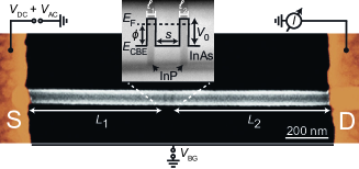
We explicitly refer to the regions of bare InAs between the QD and the source or drain contact as the lead segments (LSs). The lead segment between the QD and the source contact is long, while the lead segment between the QD and the drain contact is long. The QD and the LSs are tuned simultaneously by the back gate voltage , which shifts the conduction band edge, , relative to the Fermi energy, , to higher or lower values. For later, we use .
The inset of Figure 1 shows a TEM image of the epitaxially defined QD region in a similar NW. The two InP segments, indicated by black arrows, act as tunnel barriers with a rectangular potential profile for electrons due to the atomically sharp transitions in the material composition. The barrier height depends the band gap discontinuities and residual strain. For our NW geometry, the barrier height is predicted to be meV [34], providing a strong confinement to the electrons in the axial direction.
All measurements were performed in a dilution refrigerator with a base temperature of . We apply a DC voltage to the source electrode to correct for small offsets ( ) and superimpose an AC voltage of typically for lock-in detection, while the drain electrode is grounded and used for the current () measurement. The differential conductance was measured using standard lock-in techniques.
Characterization of the Quantum Dot
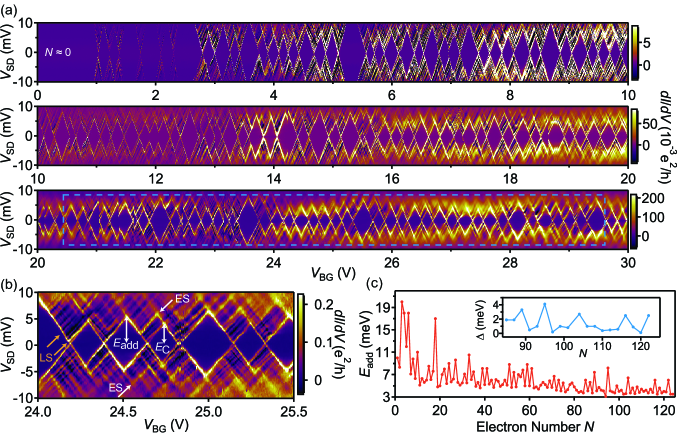
Figure 2(a) shows as a function of and . We observe regular, stable, and reproducible Coulomb diamonds (CDs) over the large backgate range of , corresponding to the addition of electrons. At , the number of electrons on the QD is close to zero, i.e. . By increasing , electrons are added to the QD sequentially, which brings the QD into the many electron regime. For the measurement sequence shown in Figure 2(a), the maximum number of electrons on the QD is . When increasing beyond , thermal activation of carriers across the tunnel barriers begins to considerably contribute to the transport.
According to the constant interaction model [42], assuming two-fold spin degenerate orbitals, the energy required to add an electron to a QD with an even electron configuration is given by the addition energy , with the charging energy, the total capacitance of the QD, and the single particle energy spacing. To add a second electron to the same QD orbital requires . This gives rise to an alternating even-odd pattern of large and small CDs, characteristic for spin-degenerate QD states, and allows one to extract the corresponding energy scales. A region of the CDs shown in Figure 2(b) exhibits a clear even-odd pattern with and , as indicated by the white arrows. From the difference between and , we find , consistent with meV from the corresponding excited state (ES) resonances outside the CDs, pointed out by white arrows.
In Figure 2(c) we plot as a function of for the full range of Figure 2(a). We find an overall decrease in for increasing due to changes in the QD capacitance by electron-electron interactions [43]. From the very regular even-odd pattern in the gate range indicated by the blue box in Figure 2(a), we extract , as shown in the inset of Figure 2(c). We find that strongly scatters and assumes values in between meV and meV, suggesting that only single levels contribute to the transport.
In addition to the QD excited state resonances, we find several other features outside of the CDs that cannot be attributed to the energy spectrum of the QD. For example, the resonances indicated by orange arrows in Figure 2(b) are due to a non-constant DOS in the LSs, forming as standing waves in the LSs. Since these waves are strongly reflected at the InP barrier, the widths of these states are determined mostly by the coupling to the source and drain contacts, respectively. In addition, we find negative differential conductance (NDC) throughout the entire gate range, which we attribute to the simutaneous tuning of the QD and the LSs with different lever arms. We note that the NDC is more prominent in the few electron regime where the carrier concentration is low. The NDC supports our notion that the DOS in the LSs is not constant, which is typical for NW QD devices with semiconductor leads [30].
Resonance Line Shapes
In this section, we extract the total tunnel coupling of the QD, , and the electron temperature in the LSs, , from the Coulomb blockade (CB) resonances. The total tunnel coupling, , is given by the individual couplings to the source and drain leads, and . In the case of an ideal measurement setup, the line shape only depends on , [44], and the asymmetry [45, 46]. However, there are also extrinsic broadening mechanisms, such as noise in the source and drain contacts, and on the gate, as well as the applied AC voltage.
For our analysis, we assume that only a single QD level contributes to the transport, i.e. ,iii is the 10%-90% width of the Fermi-Dirac distribution and account for the three main broadening contributions: , , and . limits the smallest width of the line shape that can be reliably extracted, therefore should be chosen such that . By tuning with , we can access three different regimes: thermally broadened (), lifetime broadened (), or a combination of both (). These three regimes are summarized in Figures 3(a), (c), and (e), where the lifetime broadening is indicated by the width of the blue QD levels and the thermal broadening by the width of the orange Fermi-Dirac distribution in the LSs.
We model the line shape of the CB resonances with the assumption that the DOS in the LSs is constant and discuss effects due to a non-constant DOS later. For a single energy level, the line shape of a conductance resonance is described by a resonant tunneling model [44, 47, 48]:
| (1) |
where is the number of independent parallel transport channels, the Breit-Wigner (BW) transmission function [47] with the detuning from the CB resonance centered at , and are the Fermi-Dirac distributions in the LSs. is calculated numerically. The contribution of is accounted for by evaluating Equation 1 for a sinusoidal that also electrically gates the QD. If not chosen properly, can mask the ”true” resonance and the measured resonance width is then given by .
Evolution of the Resonance Line Shapes
We now investigate how the line shapes of the resonances evolves with and the bath temperature, . Figures 3(b),(d), and (f) show high resolution CB resonance measurements in the three broadening regimes. To show the evolution of , each of the three CB resonances was fit with the expressions for a thermal, BW, and the convolution line shape, described by Equation 1. From the convolution fit, we extract , , , and their corresponding standard error of the individual fits, shown as error bars in Figure 3(g) and 4.iiiiiiThis error bar does not account for potential experimental errors in consecutive experiments.
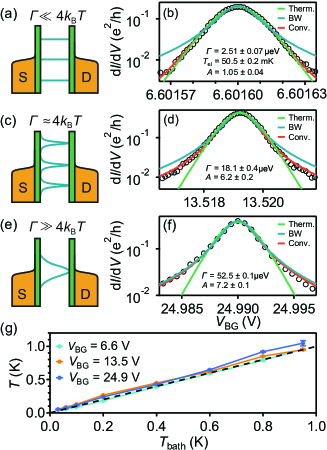
Figure 3(b) shows a CB resonance near depletion () at , measured with . The convolution line shape agrees very well with the experiment, as does the pure thermal broadening line shape, but not the BW line shape. In this regime, the conduction band edge of the LSs is near the Fermi level () and the electrons are strongly confined by the large tunnel barriers, such that the width of the Coulomb resonance is mostly determined by the electron temperature and not by the QD lifetime. Only in this regime, we can accurately determine the electron temperature of the LSs. From the convolution fit, the extracted total tunnel coupling, asymmetry, and electron temperature are , , and mK, respectively. We see that is somewhat higher than the bath temperature ( mK), probably due to noise and radiation due to insufficient filtering. Since is not expected to change with , we set mK for the following analysis of data at the same .
For the resonance at () a transition from the thermally to the lifetime broadened regime begins. As shown in Figures 3(c) and (d), only the convolution line shape fits the data well. From the convolution fit, with mK and fixed, and were extracted from the fit. Therefore, this resonance is in the regime where the lifetime and thermal broadening contributes equally significantly with .
By increasing the gate voltage further, the CB resonances transition into the lifetime broadened regime with . This can be seen for the resonance in Figure 3(f) at (), where the data agrees very well with the convolution fit, as well as with the BW fit, with mK and fixed. From the convolution fit, we extract and , which shows that the resonance is mostly lifetime broadened ().
For each of the three resonances, the temperature dependence of the CB resonances was investigated, as shown in Figure 3(g). We used the convolution fit with and fixed at the values determined at mK, to extract for a series of different . For low , the CB resonances are either thermally broadened for , lifetime broadened for , or a combination of the two for , as discussed in the previous section. For bath temperatures between and , the extracted remains constant. As we increase beyond , for two resonances (cyan and orange) increases with a slope of , in agreement with the thermally broadened regime. This is indicated by the dashed black line with a slope of . However, for the blue resonance, which is mostly lifetime broadened, the slope is , likely due to the resonance not fully transitioning into the temperature broadened regime. These experiments show that the electron and phonon system equilibrate at and that InAs/InP heterostructure QDs can be used as in-situ thermometers. In contrast to typical Coulomb blockade thermometers [49, 50], integrated QDs form an integral part of the device, which does not require thermal coupling to a separate device.
Properties of the Tunnel Barriers
By investigating the functional dependence of the total tunnel coupling and the asymmetry on , we estimate the height and symmetry of the tunnel barriers formed by the InP segments. By fitting the CB resonances with Equation 1 and using the previously determined mK, we extract and as a function of , as shown in Figures 4(a) and (b), respectively. The red data points correspond to the CB resonances from Figures 3(b),(d),and (f) measured with a high resolution in , while the black data points stem from resonances selected from a large gate sweep () over measured with a lower resolution.
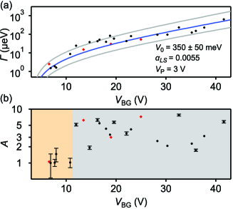
is plotted in Figure 4(a) and shows a systematic increase of with increasing . Close to full depletion, we find a tunnel coupling of , which increases up to for . Comparing the dependence of to a resonant tunneling model allows us to estimate . For this, we assume that an electron bounces back and fourth in the InAs segment between the two InP barriers at an attempt frequency and escapes through either of the barriers with a probability given by the rectangular tunnel barriers. Consequently, the total tunnel coupling as a function of can be described by [51]:
| (2) |
with , the effective electron mass in the InP segments [52], , the lever arm of the LSs, the pinch-off gate voltage, the attempt frequency with Fermi velocity , and the effective electron mass in wurzite InAs [53]. The values for the length of the InP segments and the QD were taken from the TEM analysis, with and , respectively.
From the best fit of Equation 2 to (solid blue), we obtain the free parameters meV, , and . is in good agreement with the calculated literature value of meV for strained InP in InAs NWs with our geometry [34]. The upper and lower solid gray lines are obtained using the same parameters and meV and meV, respectively. agrees very well with the first CB resonances and is times smaller than the lever arm to the QD, in qualitative agreement with the LSs being longer than the QD.
Next, we investigate the asymmetry as a function of in Figure 4(b). The values of scatter seemingly random between and for . However, for , is constant, indicating highly symmetrical tunnel barriers. These characteristics of can be understood qualitatively by the following argument. The modulation of the DOS in the confined LSs is determined by the single particle level spacing in the LSs, , and the broadening of the energy levels in the LSs, . At , for a parabolic dispersion relation and thus . In addition, the strong coupling between the LSs and the source or the drain contact gives rise to a larger than for the QD. With increasing , also increases and we suspect that for , , leading to a weaker overlap between the energy levels and thus to a stronger modulation of the DOS in the LSs. In contrast, for , decreases and the energy levels in the LSs overlap stronger, resulting in a weaker modulation of the DOS. Consequently, in the low gate regime, reflects the asymmetry of the tunnel barriers , which are essentially equal in length and height.
3 Summary and Conclusion
In summary, we present an in-depth characterization of a QD formed by InP tunnel barriers and connected to metallic contacts via NW lead segments. For this system we demonstrate a nearly depletable QD with Coulomb diamonds that are exceptionally robust against charge rearrangements over a large gate range of , corresponding to electron states, and several months measurement time. By analyzing the line shapes of the CB resonances, we find a continuous transition from the lifetime to the thermally broadened regime and extract the electron temperature in the LSs. The QD shows a systematic and tunable increase in the tunnel coupling, based on which we estimate the conduction band edge offset between the InAs and the InP segments as meV. The InP segments act like ideal tunnel barriers with an asymmetry of , as targeted in the crystal growth. This is found for low , where the modulation of the DOS in the LSs is negligible, while at larger the transport is modulated by the NW lead states. In conclusion, we demonstrate that integrated InAs/InP quantum dots are a promising platform for quantitative in situ electron tunneling spectroscopy and thermometry for future superconducting hybrid devices and other electronic and thermoelectrical applications.
Corresponding Authors
∗Email: frederick.thomas@unibas.ch
∗Email: andreas.baumgartner@unibas.ch
Author Contributions
F.T. fabricated the device and performed the measurements. F.T., A.B., M.N., and G.F. analyzed the data. C.J. supported the fabrication and performed several electrical characterization measurements on different growth batches of the InAs/InP NWs. L.G. fabricated, measured, and analyzed a similar device. G.F. performed measurements for a similar device that F.T. and C.J. fabricated. F.R., V.Z., and L.S. developed the nanowire structure. C.S. and A.B. planned and designed the experiments, and participated in all discussions. All authors contributed to the manuscript.
References
References
- [1] Alicea J, Oreg Y, Refael G, von Oppen F and Fisher M P A 2011 Nature Physics 7 412–417
- [2] Hofstetter L, Csonka S, Nygård J and Schönenberger C 2009 Nature 461 960–963
- [3] Fülöp G, Domínguez F, d’Hollosy S, Baumgartner A, Makk P, Madsen M, Guzenko V, Nygård J, Schönenberger C, Yeyati A L and Csonka S 2015 Physical Review Letters 115 227003
- [4] Nadj-Perge S, Frolov S M, Bakkers E P A M and Kouwenhoven L P 2010 Nature 468 1084–1087
- [5] Karg S F, Troncale V, Drechsler U, Mensch P, Kanungo P D, Schmid H, Schmidt V, Gignac L, Riel H and Gotsmann B 2014 Nanotechnology 25 305702
- [6] Kosaka H, Kiselev A, Baron F, Kim K W and Yablonovitch E 2001 Electronics Letters 37 464
- [7] Fasth C, Fuhrer A, Samuelson L, Golovach V N and Loss D 2007 Physical Review Letters 98 266801
- [8] Björk M T, Fuhrer A, Hansen A E, Larsson M W, Fröberg L E and Samuelson L 2005 Physical Review B 72 201307
- [9] D’Hollosy S, Fábián G, Baumgartner A, Nygård J and Schönenberger C 2013 AIP Conf. Proc. 359–360
- [10] Prete D, Erdman P A, Demontis V, Zannier V, Ercolani D, Sorba L, Beltram F, Rossella F, Taddei F and Roddaro S 2019 Nano Letters 19 3033–3039
- [11] Jiang X, Xiong Q, Nam S, Qian F, Li Y and Lieber C M 2007 Nano Letters 7 3214–3218
- [12] Nilsson M, Namazi L, Lehmann S, Leijnse M, Dick K A and Thelander C 2016 Physical Review B 94 115313
- [13] Björk M T, Ohlsson B J, Sass T, Persson A I, Thelander C, Magnusson M H, Deppert K, Wallenberg L R and Samuelson L 2002 Nano Letters 2 87–89
- [14] Dick K A, Thelander C, Samuelson L and Caroff P 2010 Nano Letters 10 3494–3499
- [15] Zannier V, Rossi F, Ercolani D and Sorba L 2019 Nanotechnology 30 094003
- [16] Gooth J, Borg M, Schmid H, Schaller V, Wirths S, Moselund K, Luisier M, Karg S and Riel H 2017 Nano Letters 17 2596–2602
- [17] Plissard S R, van Weperen I, Car D, Verheijen M A, Immink G W G, Kammhuber J, Cornelissen L J, Szombati D B, Geresdi A, Frolov S M, Kouwenhoven L P and Bakkers E P A M 2013 Nature Nanotechnology 8 859–864
- [18] Krizek F, Kanne T, Razmadze D, Johnson E, Nygård J, Marcus C M and Krogstrup P 2017 Nano Letters 17 6090–6096
- [19] Gazibegovic S, Car D, Zhang H, Balk S C, Logan J A, de Moor M W A, Cassidy M C, Schmits R, Xu D, Wang G, Krogstrup P, het Veld R L M O, Zuo K, Vos Y, Shen J, Bouman D, Shojaei B, Pennachio D, Lee J S, van Veldhoven P J, Koelling S, Verheijen M A, Kouwenhoven L P, Palmstrøm C J and Bakkers E P A M 2017 Nature 548 434–438
- [20] Krogstrup P, Ziino N L B, Chang W, Albrecht S M, Madsen M H, Johnson E, Nygård J, Marcus C M and Jespersen T S 2015 Nature Materials 14 400–406
- [21] Deng M T, Vaitiekėnas S, Prada E, San-Jose P, Nygård J, Krogstrup P, Aguado R and Marcus C M 2018 Physical Review B 98 085125
- [22] Vaitiekėnas S, Deng M T, Nygård J, Krogstrup P and Marcus C 2018 Physical Review Letters 121 037703
- [23] Chevallier D, Szumniak P, Hoffman S, Loss D and Klinovaja J 2018 Physical Review B 97 045404
- [24] Gharavi K, Hoving D and Baugh J 2016 Physical Review B 94 155417
- [25] Deng M T, Vaitiekėnas S, Hansen E B, Danon J, Leijnse M, Flensberg K, Nygård J, Krogstrup P and Marcus C M 2016 Science 354 1557–1562
- [26] Plugge S, Rasmussen A, Egger R and Flensberg K 2017 New Journal of Physics 19 012001
- [27] Leijnse M and Flensberg K 2011 Physical Review B 84 140501
- [28] Heedt S, Otto I, Sladek K, Hardtdegen H, Schubert J, Demarina N, Lüth H, Grützmacher D and Schäpers T 2015 Nanoscale 7 18188–18197
- [29] Nilsson M, Namazi L, Lehmann S, Leijnse M, Dick K A and Thelander C 2016 Physical Review B 93 195422
- [30] Björk M T, Thelander C, Hansen A E, Jensen L E, Larsson M W, Wallenberg L R and Samuelson L 2004 Nano Letters 4 1621–1625
- [31] Jünger C, Baumgartner A, Delagrange R, Chevallier D, Lehmann S, Nilsson M, Dick K A, Thelander C and Schönenberger C 2019 Communications Physics 2
- [32] Chen I J, Lehmann S, Nilsson M, Kivisaari P, Linke H, Dick K A and Thelander C 2017 Nano Letters 17 902–908
- [33] Björk M T, Ohlsson B J, Sass T, Persson A I, Thelander C, Magnusson M H, Deppert K, Wallenberg L R and Samuelson L 2002 Applied Physics Letters 80 1058–1060
- [34] Niquet Y M and Mojica D C 2008 Physical Review B 77 115316
- [35] Romeo L, Roddaro S, Pitanti A, Ercolani D, Sorba L and Beltram F 2012 Nano Letters 12 4490–4494
- [36] Cornia S, Rossella F, Demontis V, Zannier V, Beltram F, Sorba L, Affronte M and Ghirri A (Preprint http://arxiv.org/abs/1907.12324v1)
- [37] Fuhrer A, Fröberg L E, Pedersen J N, Larsson M W, Wacker A, Pistol M E and Samuelson L 2007 Nano Letters 7 243–246
- [38] Rossella F, Bertoni A, Ercolani D, Rontani M, Sorba L, Beltram F and Roddaro S 2014 Nature Nanotechnology 9 997–1001
- [39] Lindemann S, Ihn T, Bieri S, Heinzel T, Ensslin K, Hackenbroich G, Maranowski K and Gossard A C 2002 Physical Review B 66 161312
- [40] Gramich J, Baumgartner A and Schönenberger C 2015 Physical Review Letters 115 216801
- [41] Suyatin D B, Thelander C, Björk M T, Maximov I and Samuelson L 2007 Nanotechnology 18 105307
- [42] Kouwenhoven L P, Austing D G and Tarucha S 2001 Reports on Progress in Physics 64 701–736
- [43] Hirose K and Wingreen N S 1999 Physical Review B 59 4604–4607
- [44] Beenakker C W J 1991 Physical Review B 44 1646–1656
- [45] Stone A D and Lee P A 1985 Physical Review Letters 54 1196–1199
- [46] Büttiker M 1986 Physical Review B 33 3020–3026
- [47] Ihn T 2009 Semiconductor Nanostructures (Oxford University Press)
- [48] Foxman E B, McEuen P L, Meirav U, Wingreen N S, Meir Y, Belk P A, Belk N R, Kastner M A and Wind S J 1993 Physical Review B 47 10020–10023
- [49] Pekola J P, Hirvi K P, Kauppinen J P and Paalanen M A 1994 Physical Review Letters 73 2903–2906
- [50] Palma M, Scheller C P, Maradan D, Feshchenko A V, Meschke M and Zumbühl D M 2017 Applied Physics Letters 111 253105
- [51] Ihn T 2009 Semiconductor Nanostructures 347 (Oxford University Press)
- [52] Kim Y S, Hummer K and Kresse G 2009 Physical Review B 80 035203
- [53] De A and Pryor C E 2010 Physical Review B 81 155210